EP0392364A2 - Procédé de fabrication d'un dispositif semi-conducteur - Google Patents
Procédé de fabrication d'un dispositif semi-conducteur Download PDFInfo
- Publication number
- EP0392364A2 EP0392364A2 EP90106550A EP90106550A EP0392364A2 EP 0392364 A2 EP0392364 A2 EP 0392364A2 EP 90106550 A EP90106550 A EP 90106550A EP 90106550 A EP90106550 A EP 90106550A EP 0392364 A2 EP0392364 A2 EP 0392364A2
- Authority
- EP
- European Patent Office
- Prior art keywords
- silicon
- film
- terized
- charac
- layer
- Prior art date
- Legal status (The legal status is an assumption and is not a legal conclusion. Google has not performed a legal analysis and makes no representation as to the accuracy of the status listed.)
- Granted
Links
Images


Classifications
-
- H—ELECTRICITY
- H10—SEMICONDUCTOR DEVICES; ELECTRIC SOLID-STATE DEVICES NOT OTHERWISE PROVIDED FOR
- H10D—INORGANIC ELECTRIC SEMICONDUCTOR DEVICES
- H10D62/00—Semiconductor bodies, or regions thereof, of devices having potential barriers
- H10D62/10—Shapes, relative sizes or dispositions of the regions of the semiconductor bodies; Shapes of the semiconductor bodies
- H10D62/13—Semiconductor regions connected to electrodes carrying current to be rectified, amplified or switched, e.g. source or drain regions
- H10D62/149—Source or drain regions of field-effect devices
- H10D62/151—Source or drain regions of field-effect devices of IGFETs
-
- H—ELECTRICITY
- H10—SEMICONDUCTOR DEVICES; ELECTRIC SOLID-STATE DEVICES NOT OTHERWISE PROVIDED FOR
- H10D—INORGANIC ELECTRIC SEMICONDUCTOR DEVICES
- H10D64/00—Electrodes of devices having potential barriers
- H10D64/01—Manufacture or treatment
- H10D64/011—Manufacture or treatment of electrodes ohmically coupled to a semiconductor
- H10D64/0111—Manufacture or treatment of electrodes ohmically coupled to a semiconductor to Group IV semiconductors
- H10D64/0113—Manufacture or treatment of electrodes ohmically coupled to a semiconductor to Group IV semiconductors the conductive layers comprising highly doped semiconductor materials, e.g. polysilicon layers or amorphous silicon layers
-
- H—ELECTRICITY
- H10—SEMICONDUCTOR DEVICES; ELECTRIC SOLID-STATE DEVICES NOT OTHERWISE PROVIDED FOR
- H10D—INORGANIC ELECTRIC SEMICONDUCTOR DEVICES
- H10D64/00—Electrodes of devices having potential barriers
- H10D64/20—Electrodes characterised by their shapes, relative sizes or dispositions
- H10D64/23—Electrodes carrying the current to be rectified, amplified, oscillated or switched, e.g. sources, drains, anodes or cathodes
- H10D64/251—Source or drain electrodes for field-effect devices
- H10D64/258—Source or drain electrodes for field-effect devices characterised by the relative positions of the source or drain electrodes with respect to the gate electrode
-
- H—ELECTRICITY
- H10—SEMICONDUCTOR DEVICES; ELECTRIC SOLID-STATE DEVICES NOT OTHERWISE PROVIDED FOR
- H10W—GENERIC PACKAGES, INTERCONNECTIONS, CONNECTORS OR OTHER CONSTRUCTIONAL DETAILS OF DEVICES COVERED BY CLASS H10
- H10W20/00—Interconnections in chips, wafers or substrates
- H10W20/01—Manufacture or treatment
- H10W20/031—Manufacture or treatment of conductive parts of the interconnections
- H10W20/056—Manufacture or treatment of conductive parts of the interconnections by filling conductive material into holes, grooves or trenches
- H10W20/057—Manufacture or treatment of conductive parts of the interconnections by filling conductive material into holes, grooves or trenches by selectively depositing, e.g. by using selective CVD or plating
-
- H—ELECTRICITY
- H10—SEMICONDUCTOR DEVICES; ELECTRIC SOLID-STATE DEVICES NOT OTHERWISE PROVIDED FOR
- H10W—GENERIC PACKAGES, INTERCONNECTIONS, CONNECTORS OR OTHER CONSTRUCTIONAL DETAILS OF DEVICES COVERED BY CLASS H10
- H10W20/00—Interconnections in chips, wafers or substrates
- H10W20/01—Manufacture or treatment
- H10W20/071—Manufacture or treatment of dielectric parts thereof
- H10W20/092—Manufacture or treatment of dielectric parts thereof by smoothing the dielectric parts
-
- H—ELECTRICITY
- H10—SEMICONDUCTOR DEVICES; ELECTRIC SOLID-STATE DEVICES NOT OTHERWISE PROVIDED FOR
- H10W—GENERIC PACKAGES, INTERCONNECTIONS, CONNECTORS OR OTHER CONSTRUCTIONAL DETAILS OF DEVICES COVERED BY CLASS H10
- H10W20/00—Interconnections in chips, wafers or substrates
- H10W20/40—Interconnections external to wafers or substrates, e.g. back-end-of-line [BEOL] metallisations or vias connecting to gate electrodes
- H10W20/41—Interconnections external to wafers or substrates, e.g. back-end-of-line [BEOL] metallisations or vias connecting to gate electrodes characterised by their conductive parts
- H10W20/44—Conductive materials thereof
- H10W20/4451—Semiconductor materials, e.g. polysilicon
Definitions
- the present invention relates to a method of manufacturing a semiconductor device, in particular, to a method wherein a step of forming an electrode in a semiconductor integrated circuit (IC) has been improved.
- IC semiconductor integrated circuit
- FIG. 2 is a partial cross-sectional view of a conventional semiconductor IC manufactured by the direct contact method, showing a drain region of a MOS transistor (MOS FET) serving as an element of a static RAM or a mask ROM.
- MOS FET MOS transistor
- An N-type diffusion region 32 is formed in a major surface of a P-type substrate 31.
- the region 32 becomes a drain region exposing to the substrate 31.
- an insulating film 33 is deposited on the substrate 31.
- An opening is formed in the insulating film 33 so as to reach the diffusion region 32.
- a polycrystalline silicon layer is deposited over the resulting structure by a CVD (Chemical Vapor Deposition) method.
- the polycrystalline silicon layer is patterned to form a wiring layer 34.
- a method as illustrated in Figs. 3A to 3C, has been proposed.
- Fig. 3A an N-type diffusion region 42 is formed in a major surface of a P-type substrate 41.
- the region 42 becomes a drain region exposing to the substrate 41.
- an insulating film 43 is deposited on the substrate 41.
- An opening 45 is formed in the insulating film 43 so as to reach the drain region 42.
- Fig. 3B by using a selective epitaxial growth method, the opening 45 is filled with a single-crystal silicon layer 46 containing N-type impurities.
- a polycrystalline silicon layer is deposited on the resulting structure, and is patterned to form a wiring layer 44.
- the low-resistance silicon layer 46 containing the impurities serves to reduce the electric resistance between the wiring layer 44 and the drain region 42.
- the formation of the silicon layer with use of the selective growth method incurs problems relating to the prevention of precipitation of silicon on the insulating layer, the removal of precipitated silicon, etc. If parameters of conditions for the selective growth, such as reaction gas density or temperature, are set to optimal values, and cleanness in the reaction vessel is maintained, the possibility of precipitation of silicon on the insulating film is kept low, and no problem would occur.
- Fig. 4 is a cross-sectional view of another conventional semiconductor device manufactured by the above-described selective growth method.
- This semiconductor device is a dynamic RAM.
- Fig. 4 shows, in particular, an area including a drain region of a MOS transistor which constitutes the dynamic RAM.
- An N-type diffusion region (drain region) 52 is formed in a P-type substrate 51 so as to expose to the surface of the substrate 51.
- a silicon oxide film 53a and a BPSG (boron-phosphor-silicon glass) film 53b are sequentially deposited on the substrate 51.
- An opening is formed in the silicon oxide film 53a and the BPSG film 53b, and a silicon layer 56 containing impurities is filled in the opening by the selective growth method.
- an aluminum-silicon alloy layer is deposited on the resulting structure, and the alloy layer is patterned to form a wiring layer 54.
- this method is effective in reducing the electric resistance between the drain region 52 and the wiring layer 54.
- similar problems remain to be solved. Namely, dust of several ⁇ m adheres to the surface of the BPSG film, in the process of filling the opening with the silicon layer 56 by the selective growth method.
- the dust originates from a silicon thin film deposited on the inner wall of the growth apparatus, or from a quartz or silicon oxide film forming the inner wall of the apparatus.
- the silicon growth is normally performed in a vessel having a reduced pressure.
- the silicon thin film or the silicon oxide film is easily peeled at the time of supplying/exhausting the air in/from the vessel.
- the peeled film is attached on the surface of the BPSG film 53b.
- the substrate is heated up to 900°C.
- the BPSG film 53b is melted, and dust attached on the surface of the BPSG film 53b is more firmly attached on or in the film 53b.
- the dust attached firmly adhered on the underlying BPSG film 53b causes deficiencies in the wiring layer 54, such as interlayer short-circuiting or breaking of wire.
- Dust of the particle size of 1/10 or more of a distance between wires may cause deficiencies in the wiring layer, and this problem becomes more significant as the number of integrated elements increases.
- the direct contact method of forming an electrode connected to the diffusion layer cannot sufficiently reduce the electric resistance at the contact portion.
- This problem may be solved by the method of forming the opening in the interlayer insulative layer on the diffusion region, filling the silicon layer in the opening by the selective vapor deposition process, and forming the electrode.
- This method has been widely used with the miniaturization of elements.
- silicon layer is filled in the opening by the selective vapor deposition, silicon may be precipitated on the insulative layer or dust may be adhered thereon, resulting in the deficiency in wiring, such as an interlayer short-circuit, and the lowering in the manufacturing yield.
- the object of the present invention is to provide a method of manufacturing a semiconductor device, wherein wiring defects due to precipitated silicon or dust on the surface of an insulative film of the semiconductor device can be reduced, and the manufacturing yield is prevented from lowering.
- a method of manufacturing a semiconductor device comprises the steps of: performing selective vapor growth on a semiconductor substrate; and polishing a surface of an insulative film formed on said semiconductor substrate subsequent to the selective vapor growth step.
- the surface of the insulative film formed on the substrate is polished to remove the precipitated silicon or dust on the surface of the the insulative film.
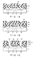
- Figs. 1A to Fig. 1F are cross-sectional views sequentially illustrating a method of manufacturing a MOS transistor, in the case where the present invention is applied to the manufacture of a static RAM, a mask ROM, etc.
- the MOS transistor is a structural element of the static RAM, mask ROM, etc.
- an element separation field oxide film 7 is selectively formed in a P-type silicon semiconductor substrate 1 having, e.g., 1 ⁇ cm, by means of a normal LOCOS (LOCal Oxidation of Silicon) method.
- a gate electrode 9 comprising a gate oxide film 8 and a polycrystalline silicon layer is formed on that area of the surface of the substrate 1 which is surrounded by the field oxide film 7.
- impurities are ion-implanted in a major surface of the substrate 1, thus forming a source region 2s and a drain region 2d exposing to the major surface of substrate 1.
- a silicon oxide film 3a having a thickness of, e.g., 3000 ⁇ is deposited on the resulting structure by means of a CVD (Chemical Vapor Deposition) method.
- a BPSG (Boron-Phosphor-Silicon Glass) layer 3b having a thickness, e.g., 7000 ⁇ is deposited on the silicon oxide film 3a.
- the BPSG film 3b is annealed in an atmosphere of POCl3 for 60 minutes at a temperature of, e.g., 950°C, so that the surface of the BPSG film 3b is flattened.
- a silicon oxide film 3c including no B (boron) or P (phosphor) having a thickness of, e.g., 1000 ⁇ is deposited on the BPSG film 3b by means of a CVD method.
- openings (contact holes or through-holes) 5s and 5d are formed in an insulative lamination film 3 (consisting of the silicon oxide film 3c, BPSG film 3b and silicon oxide film 3a) so as to reach the surfaces of the source region 2s and drain region 2d.
- a conventional PEP (photo-etching process) method e.g., reactive ion etching
- openings (contact holes or through-holes) 5s and 5d are formed in an insulative lamination film 3 (consisting of the silicon oxide film 3c, BPSG film 3b and silicon oxide film 3a) so as to reach the surfaces of the source region 2s and drain region 2d.
- silicon layers 6s and 6d doped with impurities are filled in the source contact hole 5s and the drain contact hole 5d by means of a selective growth method.
- the selective growth method is performed, for example, under the following conditions: the flow rate of H2 gas is 100/min., the flow rate of SiH2Cl2 is 400 ml/min., the flow rate of HCl gas is 1l/min., and the flow rate of PH3 gas or a doping gas is 10 ml/min.
- These gases are supplied to a reaction chamber.
- the pressure in the reaction chamber is reduced to 100 Torr, and the temperature in the chamber is set to 900°C.
- the selective growth method is performed at a temperature 900°C, an impurity of P (phosphor) contained in the doping gas is diffused into the substrate 1, thus reducing the contact resistance between the diffusion regions 2s and 2d and the silicon layers 6s and 6d is reduced.
- Fig. 1E is illustrative of the polishing process.
- a substrate (or a wafer) 21 is attached on a polishing plate 23.
- the wafer 21 is polished on a rotating table 20 on which a polishing cloth is laid.
- the polishing is carried out under a pressure of 220 g/cm2.
- a polishing material was formed in the following manner.
- the alkaline solution was mixed with water.
- the volume ratio of the alkaline solution to the water is 1 : 5.
- the polishing time was ten minutes. Under the above conditions, the degree of polished silicon oxide (SiO2) was small, i.e., 0 to 0.05 ⁇ m, compared to the degree of polished silicon (Si) which was about 1 ⁇ m.
- the entire substrate is subjected to ultrasonic rinsing with a frequency of 0.9 MHz and an output power of 500 W.
- a rinsing liquid pure water may be used.
- the alloy layer is patterned to form a source wiring layer 4s and a drain wiring layer 4d which are brought into electrical contact with the surfaces of the silicon layers 6s and 6d filled in the contact holes.
- a thickness of dust accumulated on the silicon oxide film 3c is about 1 ⁇ m.
- the above-described polishing step is a mechanical/chemical polishing step for selectively polishing the silicon. Though the silicon is polished to a large degree, the silicon oxide film is hardly be polished. Thus, substantially only the silicon particles or dust on the insulative film is removed.
- the silicon particles or dust on the silicon oxide film 3c can be removed, and the possibility of malefaction of the the wiring layer, such as short-circuiting, can be reduced.
- the yield in the wiring step is conventionally 88 %.
- the yield increases to 98 %.
- the silicon oxide film 3c is deposited after annealing the BPSG film 3b.
- any material which is less polished than silicon may be used.
- PSG (phosphor silicate glass) film, SiN (silicon nitride) film, etc. may be used.
- the silicon oxide film 3c may not be deposited. In other words, the PSG film, BPSG film are melted at a certain temperature in the selective growth step, and the silicon particles are securely attached. However, the attached particles are easily removed by the mechanical/chemical polishing method of the present invention for selectively polishing silicon.
- the MOS transistor is formed in the P-type substrate.
- the MOS transistor may be formed in a P-type well region in an N-type substrate.
- the above embodiment is directed to the manufacture of the N-channel MOS transistor.
- the present invention is applicable to the manufacture of a P-channel MOS transistor.
- this embodiment is directed to the method of manufacturing a semiconductor device such as a static RAM or a mask ROM having a MOS transistor as a structural element.
- this invention is also applicable to a method of manufacturing other type of semiconductor device having an electrode forming structure wherein a wiring layer and a diffusion layer (active layer), between which an insulative film is interposed, are connected by a silicon semiconductor layer formed by means of selective vapor deposition.
- impurities are doped in the selectively grown silicon semiconductor layer by using PH3 gas.
- the present invention can provide a method of manufacturing a semiconductor device, wherein wiring deficiencies due to precipitated silicon, etc. can be remarkably reduced, and the lowering in the manufacturing yield can be prevented.
Landscapes
- Internal Circuitry In Semiconductor Integrated Circuit Devices (AREA)
- Electrodes Of Semiconductors (AREA)
- Mechanical Treatment Of Semiconductor (AREA)
Applications Claiming Priority (2)
| Application Number | Priority Date | Filing Date | Title |
|---|---|---|---|
| JP1087954A JP2726488B2 (ja) | 1989-04-10 | 1989-04-10 | 半導体装置の製造方法 |
| JP87954/89 | 1989-04-10 |
Publications (3)
| Publication Number | Publication Date |
|---|---|
| EP0392364A2 true EP0392364A2 (fr) | 1990-10-17 |
| EP0392364A3 EP0392364A3 (fr) | 1991-03-13 |
| EP0392364B1 EP0392364B1 (fr) | 1995-11-22 |
Family
ID=13929272
Family Applications (1)
| Application Number | Title | Priority Date | Filing Date |
|---|---|---|---|
| EP90106550A Expired - Lifetime EP0392364B1 (fr) | 1989-04-10 | 1990-04-05 | Procédé de fabrication d'un dispositif semi-conducteur |
Country Status (4)
| Country | Link |
|---|---|
| EP (1) | EP0392364B1 (fr) |
| JP (1) | JP2726488B2 (fr) |
| KR (1) | KR930007095B1 (fr) |
| DE (1) | DE69023685T2 (fr) |
Cited By (1)
| Publication number | Priority date | Publication date | Assignee | Title |
|---|---|---|---|---|
| WO1999032570A1 (fr) * | 1997-12-23 | 1999-07-01 | Akzo Nobel N.V. | Composition pour polissage mecanique et chimique |
Family Cites Families (7)
| Publication number | Priority date | Publication date | Assignee | Title |
|---|---|---|---|---|
| JPS5624373B2 (fr) * | 1973-12-13 | 1981-06-05 | ||
| JPS60140818A (ja) * | 1983-12-28 | 1985-07-25 | Fujitsu Ltd | 半導体装置の製造方法 |
| FR2563048B1 (fr) * | 1984-04-13 | 1986-05-30 | Efcis | Procede de realisation de contacts d'aluminium a travers une couche isolante epaisse dans un circuit integre |
| JPS6278829A (ja) * | 1985-09-30 | 1987-04-11 | Mitsubishi Electric Corp | 半導体装置の製造方法 |
| JPS6298747A (ja) * | 1985-10-25 | 1987-05-08 | Fujitsu Ltd | 半導体装置の製造方法 |
| US4671851A (en) * | 1985-10-28 | 1987-06-09 | International Business Machines Corporation | Method for removing protuberances at the surface of a semiconductor wafer using a chem-mech polishing technique |
| JPS62291918A (ja) * | 1986-06-12 | 1987-12-18 | Matsushita Electric Ind Co Ltd | 金属の選択堆積法 |
-
1989
- 1989-04-10 JP JP1087954A patent/JP2726488B2/ja not_active Expired - Fee Related
-
1990
- 1990-04-05 EP EP90106550A patent/EP0392364B1/fr not_active Expired - Lifetime
- 1990-04-05 DE DE69023685T patent/DE69023685T2/de not_active Expired - Fee Related
- 1990-04-10 KR KR1019900004895A patent/KR930007095B1/ko not_active Expired - Fee Related
Cited By (1)
| Publication number | Priority date | Publication date | Assignee | Title |
|---|---|---|---|---|
| WO1999032570A1 (fr) * | 1997-12-23 | 1999-07-01 | Akzo Nobel N.V. | Composition pour polissage mecanique et chimique |
Also Published As
| Publication number | Publication date |
|---|---|
| DE69023685D1 (de) | 1996-01-04 |
| JPH02268425A (ja) | 1990-11-02 |
| DE69023685T2 (de) | 1996-05-09 |
| JP2726488B2 (ja) | 1998-03-11 |
| KR930007095B1 (ko) | 1993-07-29 |
| EP0392364B1 (fr) | 1995-11-22 |
| KR900017112A (ko) | 1990-11-15 |
| EP0392364A3 (fr) | 1991-03-13 |
Similar Documents
| Publication | Publication Date | Title |
|---|---|---|
| EP0415537B1 (fr) | Procédé de fabrication d'une partie de contact pour connexion d'un dispositif à semi-conducteur | |
| JP4066574B2 (ja) | 半導体装置の製造方法 | |
| US4422885A (en) | Polysilicon-doped-first CMOS process | |
| EP0068154B1 (fr) | Circuit intégré comportant un substrat semiconducteur ayant des régions d'isolation et des régions électriquement conductrices | |
| JP2861869B2 (ja) | 半導体装置の製造方法 | |
| US3400309A (en) | Monolithic silicon device containing dielectrically isolatng film of silicon carbide | |
| US5188987A (en) | Method of manufacturing a semiconductor device using a polishing step prior to a selective vapor growth step | |
| EP0076105A2 (fr) | Procédé de fabrication d'un transitor bipolair | |
| US5607875A (en) | Method of separating a semiconductor wafer with dielectrics | |
| EP0018175A2 (fr) | Procédé pour la fabrication d'une électrode sur un dispositif semiconducteur | |
| US5882990A (en) | Manufacturing method for wafer slice starting material to optimize extrinsic gettering during semiconductor fabrication | |
| EP0076106A2 (fr) | Procédé de fabrication d'un transistor bipolaire | |
| US6228728B1 (en) | Method of fabricating semiconductor device | |
| US5846869A (en) | Method of manufacturing semiconductor integrated circuit device | |
| US6087241A (en) | Method of forming side dielectrically isolated semiconductor devices and MOS semiconductor devices fabricated by this method | |
| US4444605A (en) | Planar field oxide for semiconductor devices | |
| US6525402B1 (en) | Semiconductor wafer, method of manufacturing the same and semiconductor device | |
| KR930002673B1 (ko) | 고융점금속 성장방법 | |
| JP3061891B2 (ja) | 半導体装置の製造方法 | |
| JPH04280456A (ja) | 半導体装置及びその製造方法 | |
| US5331193A (en) | Semiconductor device resistant to slip line formation | |
| EP0392364B1 (fr) | Procédé de fabrication d'un dispositif semi-conducteur | |
| US6228766B1 (en) | Process for fabricating semiconductor device without separation between silicide layer and insulating layer | |
| WO1993011558A1 (fr) | Procede de modification de la resistance de contact dans des dispositifs a semiconducteur, et articles ainsi produits | |
| JPS6160580B2 (fr) |
Legal Events
| Date | Code | Title | Description |
|---|---|---|---|
| PUAI | Public reference made under article 153(3) epc to a published international application that has entered the european phase |
Free format text: ORIGINAL CODE: 0009012 |
|
| 17P | Request for examination filed |
Effective date: 19900405 |
|
| AK | Designated contracting states |
Kind code of ref document: A2 Designated state(s): DE FR GB |
|
| PUAL | Search report despatched |
Free format text: ORIGINAL CODE: 0009013 |
|
| AK | Designated contracting states |
Kind code of ref document: A3 Designated state(s): DE FR GB |
|
| RHK1 | Main classification (correction) |
Ipc: H01L 21/304 |
|
| 17Q | First examination report despatched |
Effective date: 19930906 |
|
| GRAA | (expected) grant |
Free format text: ORIGINAL CODE: 0009210 |
|
| AK | Designated contracting states |
Kind code of ref document: B1 Designated state(s): DE FR GB |
|
| REF | Corresponds to: |
Ref document number: 69023685 Country of ref document: DE Date of ref document: 19960104 |
|
| ET | Fr: translation filed | ||
| PLBE | No opposition filed within time limit |
Free format text: ORIGINAL CODE: 0009261 |
|
| STAA | Information on the status of an ep patent application or granted ep patent |
Free format text: STATUS: NO OPPOSITION FILED WITHIN TIME LIMIT |
|
| 26N | No opposition filed | ||
| PGFP | Annual fee paid to national office [announced via postgrant information from national office to epo] |
Ref country code: FR Payment date: 19970409 Year of fee payment: 8 |
|
| PGFP | Annual fee paid to national office [announced via postgrant information from national office to epo] |
Ref country code: DE Payment date: 19970414 Year of fee payment: 8 |
|
| PG25 | Lapsed in a contracting state [announced via postgrant information from national office to epo] |
Ref country code: FR Free format text: THE PATENT HAS BEEN ANNULLED BY A DECISION OF A NATIONAL AUTHORITY Effective date: 19980430 |
|
| REG | Reference to a national code |
Ref country code: GB Ref legal event code: 746 Effective date: 19981010 |
|
| PG25 | Lapsed in a contracting state [announced via postgrant information from national office to epo] |
Ref country code: DE Free format text: LAPSE BECAUSE OF NON-PAYMENT OF DUE FEES Effective date: 19990202 |
|
| REG | Reference to a national code |
Ref country code: FR Ref legal event code: ST |
|
| REG | Reference to a national code |
Ref country code: GB Ref legal event code: IF02 |
|
| PGFP | Annual fee paid to national office [announced via postgrant information from national office to epo] |
Ref country code: GB Payment date: 20070404 Year of fee payment: 18 |
|
| GBPC | Gb: european patent ceased through non-payment of renewal fee |
Effective date: 20080405 |
|
| PG25 | Lapsed in a contracting state [announced via postgrant information from national office to epo] |
Ref country code: GB Free format text: LAPSE BECAUSE OF NON-PAYMENT OF DUE FEES Effective date: 20080405 |