EP0396892A2 - Dispositif de traitement de données - Google Patents
Dispositif de traitement de données Download PDFInfo
- Publication number
- EP0396892A2 EP0396892A2 EP90105795A EP90105795A EP0396892A2 EP 0396892 A2 EP0396892 A2 EP 0396892A2 EP 90105795 A EP90105795 A EP 90105795A EP 90105795 A EP90105795 A EP 90105795A EP 0396892 A2 EP0396892 A2 EP 0396892A2
- Authority
- EP
- European Patent Office
- Prior art keywords
- instruction
- store
- vector
- interval
- issuing
- Prior art date
- Legal status (The legal status is an assumption and is not a legal conclusion. Google has not performed a legal analysis and makes no representation as to the accuracy of the status listed.)
- Granted
Links
Images

Classifications
-
- G—PHYSICS
- G06—COMPUTING OR CALCULATING; COUNTING
- G06F—ELECTRIC DIGITAL DATA PROCESSING
- G06F15/00—Digital computers in general; Data processing equipment in general
- G06F15/76—Architectures of general purpose stored program computers
- G06F15/80—Architectures of general purpose stored program computers comprising an array of processing units with common control, e.g. single instruction multiple data processors
- G06F15/8053—Vector processors
- G06F15/8061—Details on data memory access
- G06F15/8069—Details on data memory access using a cache
-
- G—PHYSICS
- G06—COMPUTING OR CALCULATING; COUNTING
- G06F—ELECTRIC DIGITAL DATA PROCESSING
- G06F9/00—Arrangements for program control, e.g. control units
- G06F9/06—Arrangements for program control, e.g. control units using stored programs, i.e. using an internal store of processing equipment to receive or retain programs
- G06F9/30—Arrangements for executing machine instructions, e.g. instruction decode
- G06F9/38—Concurrent instruction execution, e.g. pipeline or look ahead
- G06F9/3824—Operand accessing
- G06F9/3834—Maintaining memory consistency
-
- G—PHYSICS
- G06—COMPUTING OR CALCULATING; COUNTING
- G06F—ELECTRIC DIGITAL DATA PROCESSING
- G06F9/00—Arrangements for program control, e.g. control units
- G06F9/06—Arrangements for program control, e.g. control units using stored programs, i.e. using an internal store of processing equipment to receive or retain programs
- G06F9/30—Arrangements for executing machine instructions, e.g. instruction decode
- G06F9/38—Concurrent instruction execution, e.g. pipeline or look ahead
- G06F9/3836—Instruction issuing, e.g. dynamic instruction scheduling or out of order instruction execution
- G06F9/3842—Speculative instruction execution
Definitions
- the present invention relates to a data processing apparatus capable of processing both scalar and vector instructions.
- a data processing apparatus of this type has a scalar cache memory which can be accessed by only a scalar instruction, processing according to a vector store instruction is performed for only a main memory. Therefore, if data corresponding to a store address of a vector store instruction is present in a scalar cache memory, the data is nullified to ensure data consistency. Note that nullification of data in the scalar cache memory is performed in units of blocks. This nullification processing of block data in the scalar cache memory is conventionally performed by activating nullification processing means after a vector store instruction is issued so that the means nullifies corresponding block data.
- a processing speed of a data processing apparatus using the above method (1) is inevitably reduced.
- a processing speed can be increased since instructions which can be passed are previously issued.
- the data processing apparatus using the method (2) although this is the same as the apparatus using the method (1), has a scalar cache memory which can be accessed by only a scalar instruction, nullification processing must be performed for the scalar cache memory in accordance with an vector store instruction. This nullification processing can be conventionally executed only after the vector scalar instruction is issued and therefore is an obstacle to a higher processing speed.
- the present invention has been made in consideration of the above situation, and has as its object to provide a data processing apparatus using the method (2) described above and capable of executing nullification processing of a scalar cache memory according to a vector store instruction passed by instruction passing issuing control before issuing of the vector store instruction.
- a data processing apparatus which includes buffer storing means having a scalar cache memory which can be accessed by only a scalar instruction, comprising instruction issuing means for issuing instructions in accordance with an instruction issuing order designated by a program, tentatively issuing a vector store instruction having no definitive data as an instruction not subjected to actual vector store processing, and after data is determined, finally issuing the vector store instruction as an instruction to be subjected to the actual vector store processing by interrupting the instruction issuing order, interval holding means for obtaining and holding a store interval block address to be operated by the vector store instruction tentatively issued from the instruction issuing means, passing control means for comparing a block address indicated by a scalar load/store instruction issued from the instruction issuing means with the store interval block address held by the interval holding means, if the block address falls outside the range of the store interval block addresses, enabling processing for the scalar load/store instruction, and if the block address falls within the range of the store interval
- the instruction issuing means tentatively issues the vector store instruction as an instruction not to be subjected to actual vector store processing
- the interval holding means obtains and holds a store interval block address to be operated by the tentatively issued vector store instruction
- the nullification processing means nullifies block data corresponding to a store address of the vector store instruction present in the store cache memory.
- processing for the scalar load/store instruction is enabled. If the block data is inside the interval, the processing for the scalar load/store instruction is waited until the vector store instruction is finally issued from the instruction issuing means and processed.
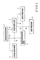
- Fig. 1 shows a main part of an embodiment of a data processing apparatus according to the present invention.
- the data processing apparatus according to this embodiment comprises an instruction issuing means 1, an interval holding means 2 connected to the instruction issuing means 1 via a tentative instruction issuing line 11, a passing control means 3 connected to the interval holding means 2 via an interval address data line 13 and connected to the instruction issuing means 1 via a final instruction issuing line 12, a nullification processing means 4 connected to the instruction issuing means 1 via the tentative instruction issuing line 11, a buffer storing means 16 connected to the nullification processing means 4 via a nullification processing data line 16 and connected to the passing control means 3 via an access signal line 14, and a main storing means 6 connected to the passing control means 3 via the access signal line 15.
- the buffer storing means 5 includes a scalar cache memory which can be accessed by only a scalar instruction. Assuming that address data is constituted by n bits of 0 to n as shown in Fig. 2 and the block size of block data of the scalar cache memory is 2 (n-m+1) , a block address is constituted by 0 to l bits, and an intrablock address is constituted by m to n bits. Note that nullification processing of the scalar cache memory is performed in units of block data.
- the instruction issuing means 1 issues an instruction in accordance with an instruction issuing order designated by a program. If a vector store instruction having no definitive data is output, the instruction issuing means 1 tentatively issues the vector store instruction as an instruction not to be subjected to actual vector store processing. After data is determined, the instruction issuing means 1 interrupts the instruction issuing order to finally issue the vector store instruction as an instruction to be subjected to the actual vector store processing. Tentative issuing of the vector store instruction is performed for the tentative instruction issuing line 11 and its final issuing is performed for the final instruction issuing line 12.
- the interval holding means 2 receives a vector store instruction tentatively issued from the instruction issuing means 1 onto the tentative instruction issuing line 11, and generates a continuous store interval address from a store start address to a store end address to be stored by the vector store instruction by using a vector store start address (B), a vector store interelement distance (D), and a vector store element number (L), all of which are designated by the vector store instruction.
- the interval holding means 2 holds address data of the store interval address except for an address part corresponding to the intrablock address shown in Fig. 2 as a store interval block address and supplies the address data to the passing control means 3 via the interval address data line 13. Note that the store interval block address held by the interval holding means 2 is erased when a corresponding vector store instruction is finally issued and processed.
- the passing control means 3 compares address data (scalar load/store block address) of a scalar load/store address indicated by a scalar load/store instruction issued from the instruction issuing means 1 except for an address part corresponding to the intrablock address shown in Fig. 2 with the store interval block address supplied from the interval holding means 2. If the scalar load/store block address falls outside the range of the store interval block address, the passing control means 3 enables the scalar load/store instruction to access the scalar cache memory of the buffer storing means 5 and the main storing means 6. If the scalar load/store block address falls within the range of the store interval block address, the passing control means 3 causes processing for the scalar load/store instruction to wait until a vector store instruction is issued from the instruction issuing means 1 and processed.
- address data scalar load/store block address
- the nullification processing means 4 nullifies block data present in the scalar cache memory of the buffer memory means 5 and corresponding to a store address of the vector store instruction by using a vector store start address (B), a vector store interelement distance (D), and a vector store element number (L), all of which are designated by the tentatively issued vector store instruction.
- B vector store start address
- D vector store interelement distance
- L vector store element number
- a vector addition instruction VADD a vector store instruction VST
- scalar load instructions LDS A and LDS B an addition instruction ADD
- a scalar store instruction STS a scalar load instruction LDS C
- store data of the vector store instruction VST indicates an arithmetic operation result of a vector addition instruction VADD of a previous instruction.
- the instruction issuing means 1 issues the respective instructions from the vector addition instruction VADD. In this case, since an arithmetic operation of the vector addition instruction VADD previous to the vector store instruction VST is not finished and the store data is not determined, the instruction issuing means 1 tentatively issues the vector store instruction VST and issues the subsequent scalar load instruction LDS A and the like in the order of addresses. Note that if the arithmetic operation by the vector addition instruction VADD is finished and the data is determined at the timing shown in Fig. 3, the vector store instruction VST is finally issued at a position indicated by a broken line in Fig. 3, i.e., next to the scalar store instruction STS by interruption.
- the interval holding means 2 calculates a store interval address ⁇ B, B + D x (L - 1) ⁇ on the basis of the vector store start address (B), the vector store interelement distance (D), and the vector store element number (L) of the vector store instruction VST.
- the interval holding means 2 generates and holds a store interval block address obtained by removing an address part corresponding to the intrablock address from the store interval address and supplies the store interval block address to the passing control means 3 via the interval address data line 13.
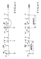
- the nullification processing means 4 obtains the nullification block addresses F0 to FN shown in Fig. 4A on the basis of the vector store start address (B), the vector store interelement distance (D), and the vector store element number (L) of the vector store instruction VST, and nullifies block data present in the store cache memory of the buffer storing means 5 and corresponding to the store address of the vector store instruction VST via the nullification processing data line 16. By this nullification, the block data corresponding to the store address of the vector store instruction VST is no longer present in the store cache memory.
- the passing control means 3 receives an instruction supplied from the instruction issuing means 1 via the final instruction issuing line 12 and executes processing such as passing control of the instruction or the like. As a series of operations, the passing control means 3 compares a scalar load/store block address indicated by the scalar load/store instruction subsequent to the tentatively issued vector store instruction VST with the store interval block address supplied from the interval holding means 2, thereby checking an address interval. If the scalar load/store block address of the scalar load/store instruction falls outside the range of the store interval block addresses, the passing control means 3 allows the scalar load/store instruction to access the buffer storing means 5 and the main storing means 6 via the access signal lines 14 and 15, respectively.
- the passing control means 3 causes the scalar load/store instruction to wait until the vector store instruction VST in a data standby state in the instruction issuing means 1 is finally issued and processed after data is determined. For example, if the subsequent scalar load instruction LDS B is to access the position of a or b in Fig. 4A, the intrablock address is discarded to update the store load address as indicated by an arrow in Fig. 4A to generate a store load block address, and the created store load block address is compared with the store interval block address. In this case, since the store load block address falls within the range of the interval, the store load instruction LDS B is waited.
- a vector store instruction to be passed by instruction passing control is tentatively issued, and processing for a scalar load/store instruction for accessing a store interval block address to be operated by the vector store instruction is waited from a timing at which the vector store instruction is tentatively issued to a timing at which it is finally issued. Therefore, nullification of a scalar cache memory according to the vector store instruction as an object to be passed can be previously controlled to increase a processing speed of the data processing apparatus.
Landscapes
- Engineering & Computer Science (AREA)
- Theoretical Computer Science (AREA)
- Software Systems (AREA)
- Physics & Mathematics (AREA)
- General Engineering & Computer Science (AREA)
- General Physics & Mathematics (AREA)
- Computer Hardware Design (AREA)
- Computing Systems (AREA)
- Memory System Of A Hierarchy Structure (AREA)
- Complex Calculations (AREA)
Applications Claiming Priority (2)
| Application Number | Priority Date | Filing Date | Title |
|---|---|---|---|
| JP75834/89 | 1989-03-28 | ||
| JP1075834A JPH0810451B2 (ja) | 1989-03-28 | 1989-03-28 | 情報処理装置 |
Publications (3)
| Publication Number | Publication Date |
|---|---|
| EP0396892A2 true EP0396892A2 (fr) | 1990-11-14 |
| EP0396892A3 EP0396892A3 (fr) | 1992-09-30 |
| EP0396892B1 EP0396892B1 (fr) | 1996-01-24 |
Family
ID=13587617
Family Applications (1)
| Application Number | Title | Priority Date | Filing Date |
|---|---|---|---|
| EP90105795A Expired - Lifetime EP0396892B1 (fr) | 1989-03-28 | 1990-03-27 | Dispositif de traitement de données |
Country Status (5)
| Country | Link |
|---|---|
| US (1) | US5247635A (fr) |
| EP (1) | EP0396892B1 (fr) |
| JP (1) | JPH0810451B2 (fr) |
| CA (1) | CA2013109C (fr) |
| DE (1) | DE69024994T2 (fr) |
Cited By (4)
| Publication number | Priority date | Publication date | Assignee | Title |
|---|---|---|---|---|
| EP0445802A3 (en) * | 1990-03-08 | 1993-11-10 | Nec Corp | Information processing apparatus |
| EP0600583A1 (fr) * | 1992-11-30 | 1994-06-08 | Fujitsu Limited | Processeur vectoriel |
| WO1997013199A1 (fr) * | 1995-10-06 | 1997-04-10 | Advanced Micro Devices, Inc. | Traitement sans ordre predetermine avec collision des operations pour reduire les delais de fonctionnement en pipeline |
| US5799165A (en) * | 1996-01-26 | 1998-08-25 | Advanced Micro Devices, Inc. | Out-of-order processing that removes an issued operation from an execution pipeline upon determining that the operation would cause a lengthy pipeline delay |
Families Citing this family (20)
| Publication number | Priority date | Publication date | Assignee | Title |
|---|---|---|---|---|
| US5418973A (en) * | 1992-06-22 | 1995-05-23 | Digital Equipment Corporation | Digital computer system with cache controller coordinating both vector and scalar operations |
| US5420991A (en) * | 1994-01-04 | 1995-05-30 | Intel Corporation | Apparatus and method for maintaining processing consistency in a computer system having multiple processors |
| US5818511A (en) * | 1994-05-27 | 1998-10-06 | Bell Atlantic | Full service network |
| US5608447A (en) * | 1994-05-27 | 1997-03-04 | Bell Atlantic | Full service network |
| US5666506A (en) * | 1994-10-24 | 1997-09-09 | International Business Machines Corporation | Apparatus to dynamically control the out-of-order execution of load/store instructions in a processor capable of dispatchng, issuing and executing multiple instructions in a single processor cycle |
| US5717895A (en) * | 1994-12-01 | 1998-02-10 | Cray Research, Inc. | Associative scalar data cache with write-through capabilities for a vector processor |
| US5826102A (en) * | 1994-12-22 | 1998-10-20 | Bell Atlantic Network Services, Inc. | Network arrangement for development delivery and presentation of multimedia applications using timelines to integrate multimedia objects and program objects |
| US5659793A (en) * | 1994-12-22 | 1997-08-19 | Bell Atlantic Video Services, Inc. | Authoring tools for multimedia application development and network delivery |
| US5854914A (en) * | 1996-02-13 | 1998-12-29 | Intel Corporation | Mechanism to improved execution of misaligned loads |
| JP3733842B2 (ja) * | 2000-07-12 | 2006-01-11 | 日本電気株式会社 | ベクトルスキャタ命令制御回路及びベクトル型情報処理装置 |
| US7577816B2 (en) * | 2003-08-18 | 2009-08-18 | Cray Inc. | Remote translation mechanism for a multinode system |
| US7743223B2 (en) * | 2003-08-18 | 2010-06-22 | Cray Inc. | Decoupling of write address from its associated write data in a store to a shared memory in a multiprocessor system |
| US8307194B1 (en) | 2003-08-18 | 2012-11-06 | Cray Inc. | Relaxed memory consistency model |
| US7543133B1 (en) | 2003-08-18 | 2009-06-02 | Cray Inc. | Latency tolerant distributed shared memory multiprocessor computer |
| US7437521B1 (en) * | 2003-08-18 | 2008-10-14 | Cray Inc. | Multistream processing memory-and barrier-synchronization method and apparatus |
| US7421565B1 (en) | 2003-08-18 | 2008-09-02 | Cray Inc. | Method and apparatus for indirectly addressed vector load-add -store across multi-processors |
| US7519771B1 (en) | 2003-08-18 | 2009-04-14 | Cray Inc. | System and method for processing memory instructions using a forced order queue |
| JP3988144B2 (ja) | 2004-02-23 | 2007-10-10 | 日本電気株式会社 | ベクトル処理装置、及び、追い越し制御回路 |
| US7478769B1 (en) | 2005-03-09 | 2009-01-20 | Cray Inc. | Method and apparatus for cooling electronic components |
| JP5206385B2 (ja) * | 2008-12-12 | 2013-06-12 | 日本電気株式会社 | バウンダリ実行制御システム、バウンダリ実行制御方法、及びバウンダリ実行制御プログラム |
Family Cites Families (9)
| Publication number | Priority date | Publication date | Assignee | Title |
|---|---|---|---|---|
| GB1443777A (en) * | 1973-07-19 | 1976-07-28 | Int Computers Ltd | Data processing apparatus |
| US4156906A (en) * | 1977-11-22 | 1979-05-29 | Honeywell Information Systems Inc. | Buffer store including control apparatus which facilitates the concurrent processing of a plurality of commands |
| US4638431A (en) * | 1984-09-17 | 1987-01-20 | Nec Corporation | Data processing system for vector processing having a cache invalidation control unit |
| US4722049A (en) * | 1985-10-11 | 1988-01-26 | Unisys Corporation | Apparatus for out-of-order program execution |
| JPH0731669B2 (ja) * | 1986-04-04 | 1995-04-10 | 株式会社日立製作所 | ベクトル・プロセツサ |
| US5063497A (en) * | 1987-07-01 | 1991-11-05 | Digital Equipment Corporation | Apparatus and method for recovering from missing page faults in vector data processing operations |
| JPS6462764A (en) * | 1987-09-03 | 1989-03-09 | Agency Ind Science Techn | Vector computer |
| US5043886A (en) * | 1988-09-16 | 1991-08-27 | Digital Equipment Corporation | Load/store with write-intent for write-back caches |
| US5123095A (en) * | 1989-01-17 | 1992-06-16 | Ergo Computing, Inc. | Integrated scalar and vector processors with vector addressing by the scalar processor |
-
1989
- 1989-03-28 JP JP1075834A patent/JPH0810451B2/ja not_active Expired - Lifetime
-
1990
- 1990-03-27 DE DE69024994T patent/DE69024994T2/de not_active Expired - Fee Related
- 1990-03-27 US US07/500,003 patent/US5247635A/en not_active Expired - Fee Related
- 1990-03-27 EP EP90105795A patent/EP0396892B1/fr not_active Expired - Lifetime
- 1990-03-27 CA CA002013109A patent/CA2013109C/fr not_active Expired - Fee Related
Cited By (5)
| Publication number | Priority date | Publication date | Assignee | Title |
|---|---|---|---|---|
| EP0445802A3 (en) * | 1990-03-08 | 1993-11-10 | Nec Corp | Information processing apparatus |
| EP0600583A1 (fr) * | 1992-11-30 | 1994-06-08 | Fujitsu Limited | Processeur vectoriel |
| US5574924A (en) * | 1992-11-30 | 1996-11-12 | Fujitsu Limited | Vector processing device that utilizes post marks to ensure serialization of access requests of vector store instructions |
| WO1997013199A1 (fr) * | 1995-10-06 | 1997-04-10 | Advanced Micro Devices, Inc. | Traitement sans ordre predetermine avec collision des operations pour reduire les delais de fonctionnement en pipeline |
| US5799165A (en) * | 1996-01-26 | 1998-08-25 | Advanced Micro Devices, Inc. | Out-of-order processing that removes an issued operation from an execution pipeline upon determining that the operation would cause a lengthy pipeline delay |
Also Published As
| Publication number | Publication date |
|---|---|
| DE69024994D1 (de) | 1996-03-07 |
| CA2013109A1 (fr) | 1990-09-28 |
| US5247635A (en) | 1993-09-21 |
| DE69024994T2 (de) | 1996-06-05 |
| EP0396892B1 (fr) | 1996-01-24 |
| EP0396892A3 (fr) | 1992-09-30 |
| JPH02253470A (ja) | 1990-10-12 |
| CA2013109C (fr) | 1996-07-30 |
| JPH0810451B2 (ja) | 1996-01-31 |
Similar Documents
| Publication | Publication Date | Title |
|---|---|---|
| EP0396892B1 (fr) | Dispositif de traitement de données | |
| US4805098A (en) | Write buffer | |
| US4530049A (en) | Stack cache with fixed size stack frames | |
| US3898624A (en) | Data processing system with variable prefetch and replacement algorithms | |
| US6779102B2 (en) | Data processor capable of executing an instruction that makes a cache memory ineffective | |
| US20050086435A1 (en) | Cache memory controlling apparatus, information processing apparatus and method for control of cache memory | |
| JPS62221036A (ja) | 計算装置 | |
| JPH0581129A (ja) | データ処理システムのキヤツシユ内のデータユニツトに対する所有権変更制御装置 | |
| JPH08194615A (ja) | 情報処理装置 | |
| JP2560988B2 (ja) | 情報処理装置および処理方法 | |
| JP3304444B2 (ja) | ベクトル処理装置 | |
| JPH01205228A (ja) | 命令バツフアシステム | |
| EP0292188B1 (fr) | Système d'antémémoire | |
| US5463737A (en) | Instruction buffer controller in processor enabling direct refetching of an instruction | |
| JPS5999552A (ja) | マイクロコンピユ−タ | |
| JPS6235694B2 (fr) | ||
| JPH0443432A (ja) | マイクロプロセッサ | |
| JPS6027418B2 (ja) | 命令先取り制御装置 | |
| JP2000194554A (ja) | 演算処理装置 | |
| JPH0399338A (ja) | マイクロプロセッサ | |
| JPH0277839A (ja) | データ処理装置 | |
| JPH03288245A (ja) | データ処理装置 | |
| JPS6072030A (ja) | 情報処理装置 | |
| JPS62241035A (ja) | 命令先取り方法 | |
| JPS6133545A (ja) | デ−タ処理装置 |
Legal Events
| Date | Code | Title | Description |
|---|---|---|---|
| PUAI | Public reference made under article 153(3) epc to a published international application that has entered the european phase |
Free format text: ORIGINAL CODE: 0009012 |
|
| 17P | Request for examination filed |
Effective date: 19900425 |
|
| AK | Designated contracting states |
Kind code of ref document: A2 Designated state(s): BE DE FR GB IT NL SE |
|
| PUAL | Search report despatched |
Free format text: ORIGINAL CODE: 0009013 |
|
| AK | Designated contracting states |
Kind code of ref document: A3 Designated state(s): BE DE FR GB IT NL SE |
|
| 17Q | First examination report despatched |
Effective date: 19941229 |
|
| GRAA | (expected) grant |
Free format text: ORIGINAL CODE: 0009210 |
|
| AK | Designated contracting states |
Kind code of ref document: B1 Designated state(s): BE DE FR GB IT NL SE |
|
| RAP2 | Party data changed (patent owner data changed or rights of a patent transferred) |
Owner name: NEC CORPORATION |
|
| REF | Corresponds to: |
Ref document number: 69024994 Country of ref document: DE Date of ref document: 19960307 |
|
| ITF | It: translation for a ep patent filed | ||
| NLT2 | Nl: modifications (of names), taken from the european patent patent bulletin |
Owner name: NEC CORPORATION |
|
| ET | Fr: translation filed | ||
| PLBE | No opposition filed within time limit |
Free format text: ORIGINAL CODE: 0009261 |
|
| STAA | Information on the status of an ep patent application or granted ep patent |
Free format text: STATUS: NO OPPOSITION FILED WITHIN TIME LIMIT |
|
| 26N | No opposition filed | ||
| PGFP | Annual fee paid to national office [announced via postgrant information from national office to epo] |
Ref country code: BE Payment date: 20000217 Year of fee payment: 11 |
|
| PGFP | Annual fee paid to national office [announced via postgrant information from national office to epo] |
Ref country code: FR Payment date: 20000310 Year of fee payment: 11 |
|
| PGFP | Annual fee paid to national office [announced via postgrant information from national office to epo] |
Ref country code: SE Payment date: 20000320 Year of fee payment: 11 |
|
| PGFP | Annual fee paid to national office [announced via postgrant information from national office to epo] |
Ref country code: GB Payment date: 20000322 Year of fee payment: 11 |
|
| PGFP | Annual fee paid to national office [announced via postgrant information from national office to epo] |
Ref country code: DE Payment date: 20000327 Year of fee payment: 11 |
|
| PGFP | Annual fee paid to national office [announced via postgrant information from national office to epo] |
Ref country code: NL Payment date: 20000330 Year of fee payment: 11 |
|
| PG25 | Lapsed in a contracting state [announced via postgrant information from national office to epo] |
Ref country code: GB Free format text: LAPSE BECAUSE OF NON-PAYMENT OF DUE FEES Effective date: 20010327 |
|
| PG25 | Lapsed in a contracting state [announced via postgrant information from national office to epo] |
Ref country code: SE Free format text: LAPSE BECAUSE OF NON-PAYMENT OF DUE FEES Effective date: 20010328 |
|
| PG25 | Lapsed in a contracting state [announced via postgrant information from national office to epo] |
Ref country code: BE Free format text: LAPSE BECAUSE OF NON-PAYMENT OF DUE FEES Effective date: 20010331 |
|
| BERE | Be: lapsed |
Owner name: NEC CORP. Effective date: 20010331 |
|
| PG25 | Lapsed in a contracting state [announced via postgrant information from national office to epo] |
Ref country code: NL Free format text: LAPSE BECAUSE OF NON-PAYMENT OF DUE FEES Effective date: 20011001 |
|
| EUG | Se: european patent has lapsed |
Ref document number: 90105795.0 |
|
| GBPC | Gb: european patent ceased through non-payment of renewal fee |
Effective date: 20010327 |
|
| PG25 | Lapsed in a contracting state [announced via postgrant information from national office to epo] |
Ref country code: FR Free format text: LAPSE BECAUSE OF NON-PAYMENT OF DUE FEES Effective date: 20011130 |
|
| NLV4 | Nl: lapsed or anulled due to non-payment of the annual fee |
Effective date: 20011001 |
|
| REG | Reference to a national code |
Ref country code: FR Ref legal event code: ST |
|
| PG25 | Lapsed in a contracting state [announced via postgrant information from national office to epo] |
Ref country code: DE Free format text: LAPSE BECAUSE OF NON-PAYMENT OF DUE FEES Effective date: 20020101 |
|
| PG25 | Lapsed in a contracting state [announced via postgrant information from national office to epo] |
Ref country code: IT Free format text: LAPSE BECAUSE OF NON-PAYMENT OF DUE FEES;WARNING: LAPSES OF ITALIAN PATENTS WITH EFFECTIVE DATE BEFORE 2007 MAY HAVE OCCURRED AT ANY TIME BEFORE 2007. THE CORRECT EFFECTIVE DATE MAY BE DIFFERENT FROM THE ONE RECORDED. Effective date: 20050327 |