EP0399513A1 - Verfahren zur Erfassung von Pitmustern - Google Patents
Verfahren zur Erfassung von Pitmustern Download PDFInfo
- Publication number
- EP0399513A1 EP0399513A1 EP90109839A EP90109839A EP0399513A1 EP 0399513 A1 EP0399513 A1 EP 0399513A1 EP 90109839 A EP90109839 A EP 90109839A EP 90109839 A EP90109839 A EP 90109839A EP 0399513 A1 EP0399513 A1 EP 0399513A1
- Authority
- EP
- European Patent Office
- Prior art keywords
- pattern
- bit data
- amplitude
- detection signal
- detection
- Prior art date
- Legal status (The legal status is an assumption and is not a legal conclusion. Google has not performed a legal analysis and makes no representation as to the accuracy of the status listed.)
- Granted
Links
Images



Classifications
-
- G—PHYSICS
- G11—INFORMATION STORAGE
- G11B—INFORMATION STORAGE BASED ON RELATIVE MOVEMENT BETWEEN RECORD CARRIER AND TRANSDUCER
- G11B7/00—Recording or reproducing by optical means, e.g. recording using a thermal beam of optical radiation by modifying optical properties or the physical structure, reproducing using an optical beam at lower power by sensing optical properties; Record carriers therefor
- G11B7/08—Disposition or mounting of heads or light sources relatively to record carriers
- G11B7/09—Disposition or mounting of heads or light sources relatively to record carriers with provision for moving the light beam or focus plane for the purpose of maintaining alignment of the light beam relative to the record carrier during transducing operation, e.g. to compensate for surface irregularities of the latter or for track following
- G11B7/0901—Disposition or mounting of heads or light sources relatively to record carriers with provision for moving the light beam or focus plane for the purpose of maintaining alignment of the light beam relative to the record carrier during transducing operation, e.g. to compensate for surface irregularities of the latter or for track following for track following only
-
- G—PHYSICS
- G11—INFORMATION STORAGE
- G11B—INFORMATION STORAGE BASED ON RELATIVE MOVEMENT BETWEEN RECORD CARRIER AND TRANSDUCER
- G11B20/00—Signal processing not specific to the method of recording or reproducing; Circuits therefor
- G11B20/10—Digital recording or reproducing
- G11B20/12—Formatting, e.g. arrangement of data block or words on the record carriers
- G11B20/1217—Formatting, e.g. arrangement of data block or words on the record carriers on discs
-
- G—PHYSICS
- G11—INFORMATION STORAGE
- G11B—INFORMATION STORAGE BASED ON RELATIVE MOVEMENT BETWEEN RECORD CARRIER AND TRANSDUCER
- G11B21/00—Head arrangements not specific to the method of recording or reproducing
- G11B21/02—Driving or moving of heads
- G11B21/08—Track changing or selecting during transducing operation
- G11B21/081—Access to indexed tracks or parts of continuous track
- G11B21/083—Access to indexed tracks or parts of continuous track on discs
-
- G—PHYSICS
- G11—INFORMATION STORAGE
- G11B—INFORMATION STORAGE BASED ON RELATIVE MOVEMENT BETWEEN RECORD CARRIER AND TRANSDUCER
- G11B27/00—Editing; Indexing; Addressing; Timing or synchronising; Monitoring; Measuring tape travel
- G11B27/10—Indexing; Addressing; Timing or synchronising; Measuring tape travel
- G11B27/19—Indexing; Addressing; Timing or synchronising; Measuring tape travel by using information detectable on the record carrier
-
- G—PHYSICS
- G11—INFORMATION STORAGE
- G11B—INFORMATION STORAGE BASED ON RELATIVE MOVEMENT BETWEEN RECORD CARRIER AND TRANSDUCER
- G11B27/00—Editing; Indexing; Addressing; Timing or synchronising; Monitoring; Measuring tape travel
- G11B27/10—Indexing; Addressing; Timing or synchronising; Measuring tape travel
- G11B27/19—Indexing; Addressing; Timing or synchronising; Measuring tape travel by using information detectable on the record carrier
- G11B27/28—Indexing; Addressing; Timing or synchronising; Measuring tape travel by using information detectable on the record carrier by using information signals recorded by the same method as the main recording
- G11B27/30—Indexing; Addressing; Timing or synchronising; Measuring tape travel by using information detectable on the record carrier by using information signals recorded by the same method as the main recording on the same track as the main recording
- G11B27/3027—Indexing; Addressing; Timing or synchronising; Measuring tape travel by using information detectable on the record carrier by using information signals recorded by the same method as the main recording on the same track as the main recording used signal is digitally coded
-
- G—PHYSICS
- G11—INFORMATION STORAGE
- G11B—INFORMATION STORAGE BASED ON RELATIVE MOVEMENT BETWEEN RECORD CARRIER AND TRANSDUCER
- G11B7/00—Recording or reproducing by optical means, e.g. recording using a thermal beam of optical radiation by modifying optical properties or the physical structure, reproducing using an optical beam at lower power by sensing optical properties; Record carriers therefor
- G11B7/004—Recording, reproducing or erasing methods; Read, write or erase circuits therefor
- G11B7/005—Reproducing
-
- G—PHYSICS
- G11—INFORMATION STORAGE
- G11B—INFORMATION STORAGE BASED ON RELATIVE MOVEMENT BETWEEN RECORD CARRIER AND TRANSDUCER
- G11B7/00—Recording or reproducing by optical means, e.g. recording using a thermal beam of optical radiation by modifying optical properties or the physical structure, reproducing using an optical beam at lower power by sensing optical properties; Record carriers therefor
- G11B7/007—Arrangement of the information on the record carrier, e.g. form of tracks, actual track shape, e.g. wobbled, or cross-section, e.g. v-shaped; Sequential information structures, e.g. sectoring or header formats within a track
- G11B7/00745—Sectoring or header formats within a track
-
- G—PHYSICS
- G11—INFORMATION STORAGE
- G11B—INFORMATION STORAGE BASED ON RELATIVE MOVEMENT BETWEEN RECORD CARRIER AND TRANSDUCER
- G11B7/00—Recording or reproducing by optical means, e.g. recording using a thermal beam of optical radiation by modifying optical properties or the physical structure, reproducing using an optical beam at lower power by sensing optical properties; Record carriers therefor
- G11B7/08—Disposition or mounting of heads or light sources relatively to record carriers
- G11B7/09—Disposition or mounting of heads or light sources relatively to record carriers with provision for moving the light beam or focus plane for the purpose of maintaining alignment of the light beam relative to the record carrier during transducing operation, e.g. to compensate for surface irregularities of the latter or for track following
- G11B7/0938—Disposition or mounting of heads or light sources relatively to record carriers with provision for moving the light beam or focus plane for the purpose of maintaining alignment of the light beam relative to the record carrier during transducing operation, e.g. to compensate for surface irregularities of the latter or for track following servo format, e.g. guide tracks, pilot signals
-
- H—ELECTRICITY
- H04—ELECTRIC COMMUNICATION TECHNIQUE
- H04L—TRANSMISSION OF DIGITAL INFORMATION, e.g. TELEGRAPHIC COMMUNICATION
- H04L7/00—Arrangements for synchronising receiver with transmitter
- H04L7/04—Speed or phase control by synchronisation signals
- H04L7/08—Speed or phase control by synchronisation signals the synchronisation signals recurring cyclically
-
- G—PHYSICS
- G11—INFORMATION STORAGE
- G11B—INFORMATION STORAGE BASED ON RELATIVE MOVEMENT BETWEEN RECORD CARRIER AND TRANSDUCER
- G11B2220/00—Record carriers by type
- G11B2220/20—Disc-shaped record carriers
-
- G—PHYSICS
- G11—INFORMATION STORAGE
- G11B—INFORMATION STORAGE BASED ON RELATIVE MOVEMENT BETWEEN RECORD CARRIER AND TRANSDUCER
- G11B2220/00—Record carriers by type
- G11B2220/20—Disc-shaped record carriers
- G11B2220/25—Disc-shaped record carriers characterised in that the disc is based on a specific recording technology
- G11B2220/2525—Magneto-optical [MO] discs
-
- G—PHYSICS
- G11—INFORMATION STORAGE
- G11B—INFORMATION STORAGE BASED ON RELATIVE MOVEMENT BETWEEN RECORD CARRIER AND TRANSDUCER
- G11B2220/00—Record carriers by type
- G11B2220/20—Disc-shaped record carriers
- G11B2220/25—Disc-shaped record carriers characterised in that the disc is based on a specific recording technology
- G11B2220/2537—Optical discs
Definitions
- This invention relates to a method for detecting pit patterns on a disk-shaped recording medium of a sampled servo system.
- a conventional disk-shaped recording medium including an optical disk or a magneto-optical disk, such as, for example, a 3.5-inch magneto-optical disk
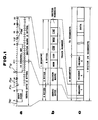
- a recording format as shown for example in Fig. 1.
- a so-called 4-11 modulation system is employed, according to which one-byte or 8-bit data are recorded by a 11 channel bit pit pattern.
- a 22 channel bit sector mark corresponding to 2-byte of data, in continuation to a 22 channel bit servo bytes corresponding similarly to 2 byte of data, at the leading position of one sector. This is a pit pattern appearing at the leading portion of each sector, as will be described in more detail later.
- the 2-byte servo bytes and the 2-byte sector mark constitute a segment along with track and sector numbers, such as MSBs and LSBs.
- the sector mark, track numbers and the sector numbers make up 8 bytes.
- each sector is constituted by 76 segments, of which the leading three segments prove to be headers 1 to 3 and the remaining 73 segments prove to be data.
- the one segment shown in Fig. 1b is arrayed at the formost one segment of the sector, that is at the header 1, as shown in Fig. 1c.
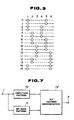
- the above one sector is organized as shown in Fig. 2, in which the header region is formed by six rows.
- the segment 1 of the header region is constituted by the 2-byte servo bytes and a 2 x 4 byte identification label ID including 2-byte sector marks, while the segment 2 is constituted by the servo bytes and the preamble/ALPC and the segment 3 by the servo bytes and the preamble.
- the data region is constituted by servo bytes and 2 x 3 byte data in 130 rows.
- the segment 68 includes 2 bytes of control data and CRC data.
- the ECC region is constituted by servo bytes and 2 x 4 bytes of ECC data in 16 rows.
- the two pits of the gray code of the servo bytes are recorded at a period of 16 tracks, as shown for example in Fig. 3.
- the bit data obtained upon reading the sector mark pits P SM constituting the sector marks are "10010010001001".
- the pit data are recorded using a pattern not usually existing in the data region.
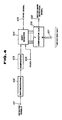
- the circuit for detecting the pit pattern of the sector marks a circuit shown in Fig. 4 is employed.
- detection signals read for example from a magneto-optical disk as the disk-shaped recording medium are input to an input terminal 101.
- the detected signal is differentiated by a differentiating circuit 102 and processed in a comparator 103 so as to be converted at a predetermined threshold level into a rectangular wave signal which is transmitted to a shift register 104.
- a sync signal and a reference clock signal are transmitted to the shift register 104 via input terminals 105 and 109, respectively, so that a signal Z produced by synchronization by the sync signal and shifting from the rectangular wave signal on the basis of the reference clock is transmitted to a comparator 106.
- a bit data pattern W of "10010010001001" is supplied to the comparator 106 via input terminal 107.
- the servo bytes and the sector mark are connected in the above format, and a pattern consisting of 14 bit intervals or 13 "0" bits between the servo bytes and the sector marks, that is a unique pattern, is formed.
- the servo bytes may be detected once for each sector.
- the actual servo bytes can be detected by the circuit having the construction similar to that of Fig. 4 when the data to be compared in the comparator 106 is the bit data pattern "100000000000001".
- predetermined pits to be detected are recorded with a predetermined radial offset from the track center and detected on the basis of a bit data pattern and an amplitude pattern of the detection signal.
- the above mentioned predetermined pit pattern may also be used for tracking servo or as at least a portion of the sector mark.
- pits recorded with a predetermined radial offset from the track center are detected and a pit pattern may be detected when the bit data and the amplitude of the detection signals of the pits represent a predetermined pattern at the time of detection.
- the servo bytes may be detected accurately by employing the pit pattern for tracking servo, whereas the sector mark may be reliably detected by constituting the sector mark by this pit pattern. That is, the pits recorded with a predetermined radial offset from the track center are detected, and the pit pattern is detected from the bit data pattern and the amplitude pattern of the detection signals of these pits at the time of detection, so that it becomes possible to reproduce a disk on which data are recorded without modulation to thereby increase the disk storage capacity.
- the servo byte or the sector marks may be detected accurately even with a disk-shaped recording medium on which data are recorded without modulation, and the pattern may be detected for each servo byte, so that capturing of the PLL may be achieved more expeditiously.
- optical disk employed in the following embodiment in an optical disk on which data have been recorded without modulation for increasing the memory capacity.
- ROM read only memory
- Fig. 5 shows an example in which a predetermined pit pattern to be detected is applied to tracking servo pits.
- a clock pit P CK is formed on a track center T kc
- a tracking pit P T1 is formed at a temporally preceding position, that is, at a position previously traversed by the laser beam with rotation of the optical disk, which is radially offset a predetermined interval d from the track center T kc towards the disk center
- a tracking pit P T2 is formed at a temporally succeeding position, that is at a position subsequently traversed by the laser beam, which is offset a predetermined interval d from the track center T kc towards the outer periphery of the disk.
- These wobbled tracking pits P T1 , P T2 and clock pit P ck represent the pit data pattern "1001001".
- the pattern of the tracking pits P T1 , P T2 and the clock pit P ck is read by an optical pickup device.
- the laser beam from the optical pick device must needs pass through the track center T kc in Fig. 5.
- the laser beam may not necessarily pass through the track center T kc but may pass through any arbitrary path. Assuming that the laser beam passes through any one of laser paths T k11 , T k12 , T kc (track center), T k01 , T k02 or T k03 , the signal detection waveforms read by the laser beam passing through these laser beam paths are as shown in Figs. 6a to 6f.
- Fig. 6a shows a signal detection waveform when the laser beam passes through the laser beam path T k11 .
- the signal detection waveform of the track pit P T1 has a large amplitude
- that of the clock pit P ck has a medium amplitude
- that of the tracking pit P T2 has a small amplitude.
- the waveform of the tracking pit P T1 has an amplitude approximately equal to that of the clock pit P ck
- the waveform of the tracking pit P T2 has a smaller amplitude.
- the waveform of the clock pit P ck has an amplitude larger than that of the waveform of P T1 and that of the waveform P T2 which are approximately equal to each other.
- the waveform of P CK has an amplitude approximately equal to that of P T2 while the waveform of P T1 has a smaller amplitude.
- the waveform of the track pit P T2 has a large amplitude, that of the clock pit P CK has a medium amplitude and that of the tracking pit P T1 has a smaller amplitude.
- the laser beam when the laser beam passes through the laser beam path T k03 , the laser beam also reads a tracking pit P T3 of the servo byte of the adjacent track.
- the waveform of the track pit P T3 has an amplitude approximately equal to the amplitude of that of the track pit P T2
- the waveform of the track pit P CK has a smaller amplitude.
- the above mentioned detection signals are supplied to the input terminal 1 and thence to a amplitude pattern detection block 70 and to a bit data pattern detection block 71.
- amplitude pattern detection block 70 amplitude data of the detection signal waveforms are taken out and compared to one another and, when any one of these signal waveforms present an amplitude pattern shown in one of Figs. 6a to 6f, a signal indicating that the amplitude pattern has been detected is transmitted to a pit pattern discrimination block 72.
- bit data are taken out from the detection signal and the pattern of the bit data of the detection signal is compared with the servo byte pit data pattern ("1001001").
- the detection block 71 transmits a signal indicating that the servo byte bit data pattern has been detected to the pit pattern discrimination block 72. That is, when the output of the block 70 and that of the block 71 are supplied to the block 72, it is determined by block 72 that the bit data pattern of the detection signal is the same as the servo byte pit pattern.
- the data pattern "1001001" in the data per se is presented with an equal amplitude of the high level signal and is not detected at the amplitude pattern detection block 70, so that it is not confused with the servo byte hit pattern shown in Fig. 5.
- FIG. 8 A typical circuit for detecting the pit pattern by applying the above mentioned pit pattern detecting method is shown in Fig. 8.
- a detection signal read at the optical pickup device from the optical disk is input to an input terminal 1.
- This detection signal is converted by an A/D converter 2 into digital wave height data which are sequentially transmitted to registers 40 to 46.
- To each of these registers 40 to 46 there are supplied from an input terminal 3 reference clocks which serve not only as bit clocks but also as channel clocks. Based on these reference clocks, the registers 40 to 46 take out amplitude data of the waveforms of the above mentioned detection signals. Amplitude date.
- a taken out from register 40 and amplitude data B taken out from register 43 are transmitted to a comparator 51, whereas the amplitude data B from register 43 and amplitude data C from register 46 are transmitted to a comparator 52 and the amplitude data A from register 40 and the amplitude data C from register 46 are transmitted to a comparator 53.
- the decoder 25 thus transmits the signal, such as "H", based on the result of comparison from the comparators 51 to 53, to an input terminal of AND gate 36.
- the detection signal is also differentiated by a differentiator 62 and converted by a comparator 63 into a rectangular wave signal at a predetermined threshold level so as to be then transmitted to a shift register 64.
- This shift register 64 is supplied from input terminal 3 with a reference clock, on the basis of which a signal X shifted from the rectangular signal is generated and transmitted to a comparator 65.
- This comparator is supplied with a bit data pattern Y "1001001".
- the differentiator circuit 62 and the comparator 63 may also be constituted by a binary circuit 26 as will be described with reference to Fig. 11.
- the signal supplied to the binary circuit 26 is the output signal from the A/D converter 2.
- An optical disk of, for example, a read only memory type is employed, as in the preceding embodiment, on which data are recorded as NRZ signal, for example, without modulation.
- the sector mark pits are formed with wobbling with respect to the track center T kc , several combinations may be conceived of those pits which are wobbled with respect to the track center T kc .
- a combination of sector mark pits P SM1 , P SM2 , P SM3 and P SM4 shown in Fig. 9 is herein explained by way of an example.
- sector mark pit P SM2 , P SM3 are formed on the track center T kc , while a sector mark pit P SM1 is formed at a position temporally preceding the sector mark pit P SM2 , that is a position traversed by the laser beam at an earlier time point with rotation of the optical disk, which position is offset a predetermined distance d radially towards the disk center, and a sector mark pit P SM4 is formed at a position temporally succeeding the sector mark pit P SM3 , which position is offset a predetermined interval d towards the outer periphery from the track center T kc .
- These wobbled sector mark pits P SM1 , P SM2 , P SM3 and P SM4 represent at bit data pattern "10010010010".
- a sector mark bit P SM5 is a sector mark pit of an adjacent track.
- the laser beam For correctly reading the sector mark, the laser beam must needs pass through the track center T kc of Fig. 9.
- the laser beam may not necessarily pass through the track center T kc , but may pass through any arbitrary path.
- the signal detection waveforms read by the laser beam passing through the laser beam paths are such as shown in Figs. 10a to 10f.
- Fig. 10a shows the detection pit pattern which is produced when the laser beam passes through laser beam path T k11
- Fig. 10b the detection pit pattern which is produced when the laser beam passes through laser beam path T k12
- Fig. 10c the detection pit pattern which is produced when the laser beam passes through laser beam path T kc
- Fig. 10d the detection pit pattern which is produced when the laser beam passes through laser beam path T k01
- Fig. 10e the detection pit pattern which is produced when the laser beam passes through laser beam path T k02
- Fig. 10f the detection pit pattern which is produced when the laser beam passes through laser beam path T k03 .
- the sector mark pits P SM1 , P SM2 , P SM3 and P SM4 are detected on the basis of the amplitude pattern and the bit data pattern of the detection signals, as described hereinabove. That is, each of the signal detection waveforms of the sector mark pits P SM1 , P SM2 , P SM3 and P SM4 presents amplitudes or heights of the signal detection waveforms shown in Figs. 10a to 10f characteristic of the laser beam paths T k11 , T k12 , T kc , T k01 , T k02 or T k03 assumed by the laser beam.
- the signal detection waveform is detected to be the sector mark when it exhibits one of the amplitude patterns shown in Figs. 10a to 10f.
- the signal detection waveform is detected to be the sector mark when on comparing the bit data of the signal detection waveform with the sector mark bit data pattern "10010010010" the bit data of the signal detection waveform is "10010010010" as is the sector mark bit data pattern.
- a pit pattern detection circuit for detecting the pit pattern according to the second embodiment is shown in Fig. 11.
- a detection signal is input to input terminal 1 and converted by A/D converter 2 into digital wave height value data which are sequentially transmitted to registers 10 to 19. To each of these registers 10 to 19, these are supplied from input terminal 3 reference clocks, based on which amplitude data of the detection signal waveforms are taken out.
- the amplitude data A taken out at the register 10 and the amplitude data B taken out at the register 13 are transmitted to a comparator 21, the amplitude data B from the register 13 and the amplitude data C from the register 16 are transmitted to a comparator 22, the amplitude data B from the register 13 and the amplitude data D from the register 19 are transmitted to a comparator 23 and the amplitude data A from the register 10 and the amplitude data D from the register 19 are transmitted to a comparator 24.
- the decoder 25 thus transmits a signal, such as signal "H", based on the results of comparison from the comparators 21 to 24, to an input terminal of the AND gate 36.
- the above mentioned wave height data are converted by a binary circuit 26, operating at the timing of reference clocks, into bit data, which are transmitted to a shift register 34.
- the reference clocks are supplied from input terminal 3 to the shift register 34, and a signal X produced by shifting the output of the binary circuit 26 on the basis of the reference clocks is transmitted to a comparator 35.
- the binary circuit 26 may be constituted by the differentiating circuit 62 and the comparator 63 as already described with reference to Fig. 8. It is the detection signal that is supplied in this case to the differentiating circuit 62 and the comparator 63.
- the servo bytes connected to the sector mark may also be detected in each sector.
Landscapes
- Engineering & Computer Science (AREA)
- Signal Processing (AREA)
- Computer Networks & Wireless Communication (AREA)
- Optical Recording Or Reproduction (AREA)
- Signal Processing For Digital Recording And Reproducing (AREA)
Applications Claiming Priority (2)
| Application Number | Priority Date | Filing Date | Title |
|---|---|---|---|
| JP1128695A JPH02308424A (ja) | 1989-05-24 | 1989-05-24 | ピットパターンの検出方法 |
| JP128695/89 | 1989-05-24 |
Publications (2)
| Publication Number | Publication Date |
|---|---|
| EP0399513A1 true EP0399513A1 (de) | 1990-11-28 |
| EP0399513B1 EP0399513B1 (de) | 1995-01-18 |
Family
ID=14991134
Family Applications (1)
| Application Number | Title | Priority Date | Filing Date |
|---|---|---|---|
| EP90109839A Expired - Lifetime EP0399513B1 (de) | 1989-05-24 | 1990-05-23 | Verfahren zur Erfassung von Pitmustern |
Country Status (4)
| Country | Link |
|---|---|
| US (1) | US5136564A (de) |
| EP (1) | EP0399513B1 (de) |
| JP (1) | JPH02308424A (de) |
| DE (1) | DE69016098T2 (de) |
Cited By (1)
| Publication number | Priority date | Publication date | Assignee | Title |
|---|---|---|---|---|
| US11232370B2 (en) | 2015-08-14 | 2022-01-25 | Hewlett-Packard Development Company, L.P. | Biometric data to facilitate learning |
Families Citing this family (4)
| Publication number | Priority date | Publication date | Assignee | Title |
|---|---|---|---|---|
| JP2625609B2 (ja) * | 1991-07-10 | 1997-07-02 | インターナショナル・ビジネス・マシーンズ・コーポレイション | ディスク記憶装置 |
| US6529451B2 (en) * | 1992-10-05 | 2003-03-04 | Mitsubishi Denki Kabushiki Kaisha | Optical disk and optical disk drive device |
| JP3306938B2 (ja) * | 1992-11-25 | 2002-07-24 | ソニー株式会社 | 同期符号抽出回路 |
| US5615205A (en) * | 1995-06-28 | 1997-03-25 | International Business Machines Corporation | Bi-level optical media having embossed header format |
Citations (4)
| Publication number | Priority date | Publication date | Assignee | Title |
|---|---|---|---|---|
| AT360253B (de) * | 1975-05-15 | 1980-12-29 | Ibm | Magnetplattenspeicher |
| EP0278006A1 (de) * | 1986-08-25 | 1988-08-17 | Sony Corporation | Plattenanordnung und plattenähnliches speichermedium |
| EP0344669A2 (de) * | 1988-05-28 | 1989-12-06 | Nec Corporation | Wiedergabeschaltung für digitale Daten für ein magnetisches Aufzeichnungsverfahren |
| EP0348949A2 (de) * | 1988-06-28 | 1990-01-03 | Nec Corporation | Plattensteuergerät |
Family Cites Families (3)
| Publication number | Priority date | Publication date | Assignee | Title |
|---|---|---|---|---|
| EP0215556B1 (de) * | 1985-07-30 | 1993-01-13 | Koninklijke Philips Electronics N.V. | Generatorkreis für Spursignal und Aufzeichnungsträger dafür |
| US4937800A (en) * | 1986-12-22 | 1990-06-26 | International Business Machines Corporation | Method of recording using selective-erasure directions for magnetooptic record members |
| JP2641491B2 (ja) * | 1988-04-15 | 1997-08-13 | パイオニア株式会社 | トラッキングエラー信号生成装置 |
-
1989
- 1989-05-24 JP JP1128695A patent/JPH02308424A/ja active Pending
-
1990
- 1990-04-18 US US07/510,826 patent/US5136564A/en not_active Expired - Fee Related
- 1990-05-23 DE DE69016098T patent/DE69016098T2/de not_active Expired - Fee Related
- 1990-05-23 EP EP90109839A patent/EP0399513B1/de not_active Expired - Lifetime
Patent Citations (4)
| Publication number | Priority date | Publication date | Assignee | Title |
|---|---|---|---|---|
| AT360253B (de) * | 1975-05-15 | 1980-12-29 | Ibm | Magnetplattenspeicher |
| EP0278006A1 (de) * | 1986-08-25 | 1988-08-17 | Sony Corporation | Plattenanordnung und plattenähnliches speichermedium |
| EP0344669A2 (de) * | 1988-05-28 | 1989-12-06 | Nec Corporation | Wiedergabeschaltung für digitale Daten für ein magnetisches Aufzeichnungsverfahren |
| EP0348949A2 (de) * | 1988-06-28 | 1990-01-03 | Nec Corporation | Plattensteuergerät |
Cited By (1)
| Publication number | Priority date | Publication date | Assignee | Title |
|---|---|---|---|---|
| US11232370B2 (en) | 2015-08-14 | 2022-01-25 | Hewlett-Packard Development Company, L.P. | Biometric data to facilitate learning |
Also Published As
| Publication number | Publication date |
|---|---|
| JPH02308424A (ja) | 1990-12-21 |
| DE69016098T2 (de) | 1995-09-07 |
| DE69016098D1 (de) | 1995-03-02 |
| US5136564A (en) | 1992-08-04 |
| EP0399513B1 (de) | 1995-01-18 |
Similar Documents
| Publication | Publication Date | Title |
|---|---|---|
| EP0603949B1 (de) | Datenaufzeichnungsgerät mit Segmentsynchronisation | |
| EP0278006B1 (de) | Plattenanordnung und plattenähnliches speichermedium | |
| WO1997039444A1 (en) | Optical disc and recording/reproducing apparatus therefor | |
| US4937804A (en) | Apparatus for recording data into optical recording medium | |
| KR940001998B1 (ko) | 광디스크의 기록재생장치 | |
| EP0390601B1 (de) | Informationsaufzeichnungsmedium und Informationsaufzeichnungs/-Wiedergabemethode und -vorrichtung, die dergleichen verwendet | |
| JPH05159462A (ja) | 情報伝送または記録方法、情報記録再生装置および情報伝送装置 | |
| EP1519379B1 (de) | Optisches aufzeichnungsmedium, informationsverarbeitungseinrichtung mit dem aufzeichnungsmedium und datenaufzeichnungsverfahren | |
| EP0544017B1 (de) | Verfahren zur aufzeichnung auf eine scheibe | |
| EP0299742A2 (de) | Optische Platte | |
| US5689488A (en) | Optical disc system, optical disc and recording method | |
| EP0399513B1 (de) | Verfahren zur Erfassung von Pitmustern | |
| JP3432003B2 (ja) | 情報再生装置及び情報記録再生装置 | |
| US8792316B2 (en) | Record carrier of the optical type and a device for recording and/or playback for use with such a record carrier | |
| JPS61168173A (ja) | 記録再生方式 | |
| US7158472B2 (en) | Record carrier and apparatus for scanning the record carrier | |
| US5270878A (en) | Magnetic recording and reproducing apparatus | |
| US6952381B2 (en) | Record carrier including a servo track having first and second modulated parts representing a data type and a word sync type, respectively, and an apparatus for scanning the record carrier | |
| US6259660B1 (en) | Optical disk apparatus having error correction circuit | |
| EP1081706A2 (de) | Datenaufzeichnungsvorrichtung zur Reduzierung einer Gleichstromkomponente und entsprechendendes Verfahren | |
| JP3443852B2 (ja) | セクタマーク検出装置 | |
| JP2798202B2 (ja) | 光ディスク装置 | |
| JP2000048493A (ja) | 光ディスクのid認識装置及び方法 | |
| JPH0581770A (ja) | 光学的記録再生装置 | |
| JPH09120542A (ja) | 光ディスクの再生方法 |
Legal Events
| Date | Code | Title | Description |
|---|---|---|---|
| PUAI | Public reference made under article 153(3) epc to a published international application that has entered the european phase |
Free format text: ORIGINAL CODE: 0009012 |
|
| AK | Designated contracting states |
Kind code of ref document: A1 Designated state(s): DE FR GB NL |
|
| 17P | Request for examination filed |
Effective date: 19901108 |
|
| 17Q | First examination report despatched |
Effective date: 19930722 |
|
| GRAA | (expected) grant |
Free format text: ORIGINAL CODE: 0009210 |
|
| AK | Designated contracting states |
Kind code of ref document: B1 Designated state(s): DE FR GB NL |
|
| REF | Corresponds to: |
Ref document number: 69016098 Country of ref document: DE Date of ref document: 19950302 |
|
| ET | Fr: translation filed | ||
| PLBE | No opposition filed within time limit |
Free format text: ORIGINAL CODE: 0009261 |
|
| STAA | Information on the status of an ep patent application or granted ep patent |
Free format text: STATUS: NO OPPOSITION FILED WITHIN TIME LIMIT |
|
| 26N | No opposition filed | ||
| PGFP | Annual fee paid to national office [announced via postgrant information from national office to epo] |
Ref country code: FR Payment date: 19970513 Year of fee payment: 8 |
|
| PGFP | Annual fee paid to national office [announced via postgrant information from national office to epo] |
Ref country code: GB Payment date: 19970514 Year of fee payment: 8 |
|
| PGFP | Annual fee paid to national office [announced via postgrant information from national office to epo] |
Ref country code: NL Payment date: 19970529 Year of fee payment: 8 |
|
| PGFP | Annual fee paid to national office [announced via postgrant information from national office to epo] |
Ref country code: DE Payment date: 19970530 Year of fee payment: 8 |
|
| PG25 | Lapsed in a contracting state [announced via postgrant information from national office to epo] |
Ref country code: GB Free format text: LAPSE BECAUSE OF NON-PAYMENT OF DUE FEES Effective date: 19980523 |
|
| PG25 | Lapsed in a contracting state [announced via postgrant information from national office to epo] |
Ref country code: FR Free format text: LAPSE BECAUSE OF NON-PAYMENT OF DUE FEES Effective date: 19980531 |
|
| PG25 | Lapsed in a contracting state [announced via postgrant information from national office to epo] |
Ref country code: NL Free format text: LAPSE BECAUSE OF NON-PAYMENT OF DUE FEES Effective date: 19981201 |
|
| GBPC | Gb: european patent ceased through non-payment of renewal fee |
Effective date: 19980523 |
|
| NLV4 | Nl: lapsed or anulled due to non-payment of the annual fee |
Effective date: 19981201 |
|
| PG25 | Lapsed in a contracting state [announced via postgrant information from national office to epo] |
Ref country code: DE Free format text: LAPSE BECAUSE OF NON-PAYMENT OF DUE FEES Effective date: 19990302 |
|
| REG | Reference to a national code |
Ref country code: FR Ref legal event code: ST |