EP0401763A2 - Système pour produire un signal d'horloge - Google Patents
Système pour produire un signal d'horloge Download PDFInfo
- Publication number
- EP0401763A2 EP0401763A2 EP90110637A EP90110637A EP0401763A2 EP 0401763 A2 EP0401763 A2 EP 0401763A2 EP 90110637 A EP90110637 A EP 90110637A EP 90110637 A EP90110637 A EP 90110637A EP 0401763 A2 EP0401763 A2 EP 0401763A2
- Authority
- EP
- European Patent Office
- Prior art keywords
- instruction
- output
- address
- flip
- timer
- Prior art date
- Legal status (The legal status is an assumption and is not a legal conclusion. Google has not performed a legal analysis and makes no representation as to the accuracy of the status listed.)
- Granted
Links
Images


Classifications
-
- G—PHYSICS
- G06—COMPUTING OR CALCULATING; COUNTING
- G06F—ELECTRIC DIGITAL DATA PROCESSING
- G06F9/00—Arrangements for program control, e.g. control units
- G06F9/06—Arrangements for program control, e.g. control units using stored programs, i.e. using an internal store of processing equipment to receive or retain programs
- G06F9/22—Microcontrol or microprogram arrangements
-
- H—ELECTRICITY
- H04—ELECTRIC COMMUNICATION TECHNIQUE
- H04J—MULTIPLEX COMMUNICATION
- H04J3/00—Time-division multiplex systems
- H04J3/02—Details
- H04J3/06—Synchronising arrangements
- H04J3/0635—Clock or time synchronisation in a network
- H04J3/0685—Clock or time synchronisation in a node; Intranode synchronisation
-
- G—PHYSICS
- G06—COMPUTING OR CALCULATING; COUNTING
- G06F—ELECTRIC DIGITAL DATA PROCESSING
- G06F1/00—Details not covered by groups G06F3/00 - G06F13/00 and G06F21/00
- G06F1/04—Generating or distributing clock signals or signals derived directly therefrom
Definitions
- the present invention relates to a timing signal generating system suitable for equipment control which requires a large number of timing signals having a constant period, such as for TDMA digital automobile telephone (land mobile radio telephone) control, general sequence control, and the like.
- timing signal having a constant period is required in many cases.
- systems for generating this timing signal there are two types of systems including one type of system which generates the timing signal solely by hardware, and the other type which generates the timing signal by using both hardware and software. The latter is superior to the former in wide use applicability and flexibility in specification modification.
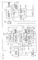
- FIG. 2 shows a simplified block diagram for the block diagram of the prior art system shown on page 19 of the above-mentioned document.
- reference numeral 21 designates a timer for generating output reference time
- numeral 22 designates an associative memory of 8 words.
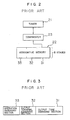
- One word of the 8 words, as shown in Fig. 3 is basically made up of an output time assigning section 31, an output terminal assigning section 32, and an operation assigning section 33.
- the reference numeral 23 designates a comparator for comparing an output of the timer 21 with the output time assigning section 31 in the associative memory 22.
- timing signal 41 as shown in Fig. 4 is generated from a terminal termed as a terminal A
- a timing signal 42 is generated from a terminal termed as a terminal B.
- the time n1, n2, n3 and n4 at which changes 43, 44, 45 and 46 of the timing signals 41 and 42 are made to occur, the nature of the signal changes at that time, and names of terminals from which the changes are generated are stored in advance in the associative memory 22 as shown in Fig. 5.
- an output of the timer 21 is compared with all the data of the output time assigning section 31 of the associative memory 22 by the comparator 23, and, when a coincidence is obtained in the comparison, a change assigned by the operation assigning section 33 is made to occur at a terminal assigned by the output terminal assigning section 32, and thus, the timing signals 41 and 42 are generated.
- timing signal generating system after the timer 21 is incremented and before the next increment is performed, it is necessary to complete the comparison operation of the output of the timer 21 with the all data of the output time assigning section 31 of the associative memory 22. For this reason, it is difficult to manufacture a system for generating a timing signal which has many changing points based on the idea mentioned above. More specifically, in the prior art example, although a timing signal having an accuracy of 2 micro seconds can be generated, since the number of words of the associative memory 22 is eight, a problem has been involved in that it is impossible to generate a timing signal having changing points exceeding eight.
- timing signal generating system in which the generation of a timing signal can be described by software and the timing signal having many changing points can be generated.
- a timing signal generating system generates a plurality of timing signals by execution of an instruction which describes timing signal changes, and the timing signal generating system comprises the following features:
- the first and the second instruction execution requesting means independently request to the execution means the execution of the instruction, and the timing signal is generated by the execution of the instruction in the instruction memory, which instruction describes changing points of the timing signal.
- the first instruction execution requesting means controls the instruction execution based on the output of the timer, and when the output of the timer indicates a desired value, the first instruction execution requesting means requests the execution.
- the second instruction execution requesting means can control the instruction execution, based on a waiting time before the execution of a next instruction which waiting time is indicated by the executed instruction itself.
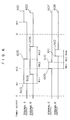
- Fig. 1 shows a first embodiment of the present invention. Before explaining the structure, the idea of a timing signal generating method which is a basic concept of a timing signal generating system of the present invention will be described.
- positions of signal changing points can be defined only by the absolute time, and in many cases, the positions can be defined by a relative relationship between the changing points.
- the positions of the changing points 604, 605 and 606 can be defined by relative time intervals Mt1, Mt2 and Mt3 from the changing points 603, 604 and 605 which are respectively preceding by one changing point.
- the positions of the changing points 610, 611 and 612 can be defined by relative time intervals Mt4, Mt5 and Mt6 respectively from the changing points 609, 610 and 611 preceding by one changing point.
- the timing signal generating system is arranged based on the idea of controlling the timing signal changes only by the absolute time such as At1 and At2.
- the timing signal generating system is arranged based on the idea that the timing signal changing positions can be controlled by both the absolute time such as At1 and At2 and the relative time intervals such as Mt1, Mt2, ..., Mt6.
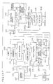
- the generation of changes (for example, the changing points 603 and 609 shown in Fig. 6) defined by the absolute time is controlled by an arrangement centering around a timer 106 and a start register 107, and the generation of changes (for example, the changing points 604 to 606 and 610 to 612) defined by the relative time intervals is controlled by an arrangement centering around a work register 112 and a zero detector 118.
- reference numeral 101 designates an instruction memory, and the timing signals shown in Fig. 6 are generated by executing instructions stored in the instruction memory 101. More specifically, by executing the instructions, the timing signal changes 603 to 606 and 609 to 612 are generated.
- the instruction as shown in Fig. 7, is made up of a terminal assigning section 71 for assigning a terminal name which performs operation, a terminal operation assigning section 72 for assigning the content which is outputted from the selected terminal, a waiting time assigning section 73 for assigning a waiting time until the next change occurs, and a condition section 74 for assigning whether an operation of the terminal is to be performed or not by judging an external condition.
- instructions 81 to 88 for generating individual changes as shown in Fig. 8 are stored at addresses beginning with an n address of the instruction memory 101.
- Reference numeral 102 designates a decoder which decodes a terminal name designated by the terminal assigning section 71 of the instruction, and when an execution request signal 128 described later is at a "1" level, the decoder 102 outputs a write signal to a flip-flop 105 corresponding to the terminal name.
- Reference numeral 103 designates a condition judging section which judges an external condition when the condition section 74 of the instruction is at a "1" level, and when the external condition is “1", the condition judging section 103 outputs a "1" level, whereas when the external condition is "0", a "0" level is outputted. However, when the condition section 74 of the instruction is "0", the condition judging section 103 does not judge the external condition and always outputs a "1" level.
- Reference numeral 104 designates a decoder which outputs a value of Table 1 described later in accordance with an output of the terminal operation assigning section 72 of the instruction and an output of the condition judging section 103.
- Reference numeral 105 designates a flip-flop including a plurality of flip-flop circuits respectively outputting terminal signals, and the flip-flop 105 receives a write signal from the decoder 102 and receives write data from the decoder 104.
- Reference numeral 106 designates a timer which generates output standard time having a constant period, and the content of the timer 106 is increased in response to an increment signal supplied externally.
- Reference numeral 107 designates a start register for executing an instruction in accordance with the absolute time generated by the timer 106, and the start register 107 includes a time section 108 and an address section 109.
- the absolute time At1 corresponding to the changing point 603 and an address n of the instruction memory 101, at which the instruction 81 is stored are stored in one register 91 which constitutes a part of the start register 107.
- the absolute time At2 corresponding to the changing point 609 and an address n + 4 of the instruction memory 101, at which the instruction 85 is stored are stored in the other register 92 which constitutes the other part of the start register 107.
- the start register 107 is constituted by two words as shown in Fig. 9.
- Reference numeral 110 designates a comparator for comparing an output of the timer 106 with all data of the time section 108 of the start register 107, and, when both the output and the data are coincident with each other, the comparator 110 outputs a coincidence signal 111 which assumes a "1" level.
- Reference numeral 112 designates a work register which is used to generate the changing points 604 to 606 and 610 to 612 as shown in Fig. 6, that is, to generate next timing signal changes based on relative time intervals from changing points respectively preceding by one changing point.
- the work register 112 includes a waiting time section 113 which takes, as an initial value, the value of the waiting time assigning section 73 of the instruction outputted from the instruction memory 101, an address section 114 which takes, as an initial value, the value of the address section 109 added with one.
- the value of the address section 109 is outputted from the start register 107.
- the address section 114 outputs the address therein to the instruction memory 101.
- the work register 112 further includes a flag section 115 for indicating by a value of "1" that the contents of both the waiting time section 113 and the address section 114 are effective.
- the output of the flag section 115 becomes a read flag signal 116.
- the work register 112 is provided with the same number of words (two words in this embodiment) as the start register 107, and the content of the work register 112 is read out, operated, and written in synchronism with the increment of the timer 106.
- Reference numeral 117 designates a decrementer for decrementing the content of the waiting time section 113 of the work register 112 in synchronism with the increment of the timer 106.
- Reference numeral 118 designates a zero detector for judging whether the content of the waiting time section 113 of the work register 112 is zero or not, and the zero detector 118 outputs a zero detection signal 119 which assumes a "1" level when zero is detected.
- Reference numeral 120 designates an incrementer which adds 1 to the output of a multiplexer 124 described later when an execution request signal 128 described later is at a "1" level, and adds 0 to the output of the multiplexer 124 when the execution request signal 128 is at a "0" level.
- Reference numeral 121 designates a zero detector which judges whether the waiting time section 73 of the instruction which is an output of the instruction memory 101 is zero or not, and when zero is detected, a zero detection signal 122 which assumes a "1" level is outputted.
- Reference numerals 123, 124, 125, and 126 respectively designate multiplexers.
- Reference numeral 127 designates a control unit which, on the basis of the coincidence signal 111, read flag signal 116, zero detection signals 119 and 122 supplied thereto and by reference to Tables 2, 3, 4, 5 and 6 described later generates the execution request signal 128 in accordance with a relationship shown in Table 2, performs input selection of the multiplexer 123 in accordance with a relationship shown in Table 3, performs input selection of the multiplexer 124 in accordance with a relationship shown in Table 4, performs input selection of the multiplexers 125 and 126 in accordance with a relationship shown in Table 5, and generates a write flag signal 129 which is an input signal to the flag section 115 of the work register 112 in accordance with a relationship shown in Table 6.
- Table 1 Input/output relationship of decoder 104 output of condition judging section 103 remarks "1" “0” output of terminal operation assigning section 72 assign "1" output 1 0 Case a assign "0" output 0 1 case b Table 2
- the case of outputting execution request signal 128 coincidence detection signal 111 read flag signal 116 zero detection signal 119 Case a 1 0 - Case b - 1 1
- Table 3 Input selection of multiplexer 128 read flag signal 116 selected input 0 A side 1 B side
- Table 4 Input selection of multiplexer 124 selected condition selected input except following case A side case a in Table 2 occurs B side
- Table 5 Input selection of multiplexer 125 and 126 selected condition selected input except following case A side cases a and b in Table 2 occur B side Table 6
- Write flag signal 129 case write flag signal 129 cases a and b in Table 2 occur, and zero detection signal 122 is 0 1 except above cases 0
- timing signal generating system arranged as mentioned above will be described by way of example in which the timing signals shown in Fig. 6 are generated.
- the flag section 115 of the work register 112 has been reset beforehand.
- the time section 108 of the start register 107 is compared with an output of the timer 106.
- the coincidence signal 111 which is at a "1" level is outputted from the comparator 110 to the control unit 127, and the following operation 1 is carried out.
- the control unit 127 selects an A side input of the multiplexer 123 in accordance with Table 3.
- a value n of the address section 109 within the start register 107 is outputted to the instruction memory 101, and an instruction 81 at an n address shown in Fig. 8 is outputted from the instruction memory 101.
- the control unit 127 delivers the execution request signal 128 to the decoder 102.
- the decoder 102 decodes the terminal assigning section 71 of the instruction 81 to determine a terminal A, and delivers a write signal to a flip-flop circuit corresponding to the terminal A among the plurality of flip-flop circuits constituting the flip-flop 105.
- the decoder 104 decodes the terminal operation assigning section 72 of the instruction 81 and also decodes an output of the condition judging section 103 thereby to generate write data to be supplied to the selected flip-flop circuit of the flip-flop 105.
- the condition assigning section 74 of the instruction 81 is "0" as shown in Fig. 8
- the external condition is not judged and a "1" level is outputted from the condition judging section 103
- the terminal operation assigning section 72 assigns an output of "1”
- the write data to the flip-flop circuit of the flip-flop 105 corresponding to the terminal A is at a "1" level according to Table 1.
- control unit 127 Since the control unit 127 has delivered the execution request signal 128 in accordance with the case a in Table 2, the control unit 127 outputs a signal (not shown) to the multiplexer 124 to select a B side input in accordance with Table 4, and the incrementer 120 is instructed to add by 1. Thus, 1 is added to n which is the output of the address section 109 of the start register 107 and the resultant n + 1 is written into the address section 114 of the work register 112.
- control unit 127 outputs a signal (not shown) to the multiplexer 125 to select a B side input in accordance with Table 5.
- a value Mt1 of the waiting time assigning section 73 of the instruction 81 shown in Fig. 8 is supplied to the decrementer 117 via the multiplexer 125.
- n + 1 is written into the address section 114 of the work register 112
- a value Mt1 - 1 is written into the waiting time section 113 of the work register 112.
- the control unit 127 outputs a signal (not shown) to the multiplexer 126 to select a B side input in accordance with Table 5.
- the control unit 127 outputs the write flag signal 129 at a "1" level in accordance with Table 6.
- "1" is written in the flag section 115 of the work register 112 at the same time when "n + 1" is written in the address section 114 thereof.
- the waiting time section 113 of the work register 112 is subtracted by 1 by the decrementer 117, and then the waiting time section 113 is again written in.
- the value Mt1 - 1 which has been written in previously becomes Mt1 - 2, Mt1 - 3, ... in synchronism with the increment of the timer 106, and it becomes eventually zero.
- the zero detection signal 119 which has a "1" level is outputted from the zero detector 118 to the control unit 127, and the following operation 2 is carried out.
- the control unit 127 selects a B side input of the multiplexer 123 in accordance with Table 3.
- an output n + 1 of the address section 114 of the work register 112 is delivered to the instruction memory 101, and an instruction 82 at n + 1 address is outputted from the instruction memory 101 as shown in Fig. 8.
- the control unit 127 delivers the execution request signal 128 to the decoder 102.
- the decoder 102 decodes the terminal assigning section 71 of the instruction 82 to determine a terminal B as shown in Fig. 8, and the decoder 102 delivers a write signal to a flip-flop circuit corresponding to the terminal B among the plurality of flip-flop circuits constituting the flip-flop 105.
- write data to the selected flip-flop circuit of the flip-flop 105 is generated by the decoder 104 by decoding the terminal operation assigning section 72 of the instruction 82 and by decoding an output of the condition judging section 103.
- the condition assigning section 74 of the instruction 82 is "0"
- the external condition is not judged
- "1" is outputted from the condition judging section 103.
- the terminal assigning section 72 assigns an output of "1”
- write data to a flip-flop circuit of the flip-flop 105 corresponding to the terminal B is "1" in accordance with Table 1.
- control unit 127 Since the control unit 127 has delivered the execution request signal 128 in accordance with the case b in Table 2, the control unit 127 outputs a signal (not shown) to the multiplexer 124 to select an A side input in accordance with Table 4, and the incrementer 120 is instructed to add by 1. Thus, "1" is added to n + 1 which is the output of the address section 114 of the work register 112, and the resultant n + 2 is written into the address section 114 of the work register 112.
- control unit 127 outputs a signal (not shown) to the multiplexer 125 to select the B side input in accordance with Table 5.
- a value Mt2 of the waiting time assigning section 73 of the instruction 82 shown in Fig. 8 is supplied to the decrementer 117 via the multiplexer 125.
- n + 2 is written into the address section 114 of the work register 112
- a value Mt2 - 1 is written into the waiting time section 113 of the work register 112.
- the control unit 127 outputs a signal (not shown) to the multiplexer 126 to select the B side input in accordance with Table 5.
- the control unit 127 outputs the write flag signal 129 at a "1" level in accordance with Table 6.
- "1" is written in the flag section 115 of the work register 112 at the same time when "n + 2" is written into the address section 114 thereof.
- the waiting time section 113 of the work register 112 is subtracted by 1 by the decrementer 117, and then the waiting time section 113 is again written in.
- the value Mt2 - 1 which has been written in previously becomes Mt2 - 2, Mt2 - 3, ..., in synchronism with the increment of the timer 106, and it becomes eventually zero.
- the zero detection signal 119 which is at a "1" level, is outputted from the zero detector 118 to the control unit 127, and the operation 2 is again carried out from item 1) described above with respect to an instruction 83 at n + 2 address within the instruction memory 101.
- the control unit 127 in the Operation 2, item 5) described above and in accordance with Table 6, writes a "0" level signal into the flag section 115 of the work register 112 in order to indicate that the contents of the waiting time section 113 and the address section 114 of the work register 112 are invalid.
- the flag section 115 is brought into a state same as the state just before the above-mentioned operation 1 is carried out. Under this state, when the output of the timer 106 indicates the value At1 again, the operation 1 is carried out again.
- timing signals 607 and 608 are outputted from terminals C and D.
- a register which is not used for the generation of the timing signals 601 and 602, is used.
- a waiting time before the execution of a next instruction is stated in an instruction, and the work register 112, the decrementer 117, the zero detector 118, etc. supervise the waiting time stated in the instruction.
- timing signals 601 and 602 in Fig. 6 maintaining their relative relationship as they are, it is only required to change the content of the time section 108 of the start register 107.
- Fig. 10 shows a block diagram of a second embodiment of the invention.
- the block diagram of Fig. 10 differs from the block diagram of Fig. 1 in that a further flip-flop 1001 is provided after the flip-flop 105.
- Fig. 11 shows a detailed arrangement of the flip-flops 105 and 1001.
- data inputs (D inputs) of the flip-flop 105 are controlled by the output of the decoder 104, and timing inputs (T inputs) are controlled by the output of the decoder 102.
- data inputs (D inputs) of the flip-flop 1001 are connected to Q outputs of the flip-flop 105, and timing inputs (T inputs) are connected to a timer increment signal which increments the timer 106.
- reference numerals 1101 and 1102 designate concrete flip-flop circuits which constitute the flip-flop 105
- reference numerals 1103 and 1104 designate concrete flip-flop circuits which constitute the flip-flop 1001.
- the operation of the timing signal generating system arranged as mentioned above will be described.
- the operation of the timing signal generating system is the same as that of the system of Fig. 1 up to the operation of the flip-flop 105, and the description will be omitted.
- the operation of the flip-flop 1001 will be described.
- a case will be considered in which the flip-flop 1101 is operated due to the execution of the instruction, and a timing signal 1201 is generated as shown in Fig. 12.
- the D input of the flip-flop circuit 1103 is connected to the Q output of the flip-flop circuit 1101, and the T input is connected to the timer increment signal.
- the Q output of the flip-flop circuit 1103 is changed in synchronism with the timer increment signal, and a timing signal 1202 is generated. Similarly, when the Q output of the flip-flop circuit 1102 generates a timing signal 1203, the Q output of the flip-flop circuit 1104 outputs a timing signal 1204 which is in synchronization with the timer increment signal.
- the flip-flop 1001 having the T inputs connected to receive the timer increment signal, irrespective of the fact that the timing of output changes of the flip-flop 105 is dependent on the timing of instruction execution, it is possible to give an appearance such that the timing signals are changing uniformly with the accuracy of the timer increment signal provided externally.
- Fig. 13 is a block diagram of a third embodiment of the present invention.
- the differences between the block diagram of Fig. 13 and the diagram of Fig. 10 reside in that an instruction memory 1303 has a bit width increased by 1 bit as compared with the instruction memory 101, and a decoder 1302, a decoder 1305, and a flip-flop 1306 are respectively changed to some extent as compared with the decoder 104, the decoder 102, and the flip-flop 105, and that an operation, which can be assigned by the terminal operation assigning section 72 of the instruction, is added.
- Table 7 shown below indicates a relationship between an input of the decoder 1302 and an output signal 1303 which is a data input to the flip-flop 105.
- cases c and d represent the added terminal operation mentioned above.
- the decoder 1302 differing from the decoder 104 outputs a write enabling signal 1304 to the decoder 1305, and this is shown in Table 8.
- Table 7 Output signal 1303 of decoder 1302 output of condition judging section 103 remarks "1" "0" output of terminal operation assigning section 72 "1" output is assigned 1 0 case a "0" output is assigned 0 1 case b AND result is assigned don't care 0 case c OR result is assigned 1 don't care case d
- Table 8 Write enabling signal 1304 outputted from decoder 1302 output of condition judging section 103 remarks "1" "0" output of terminal operation assigning section 72 "1” output is assigned 1 case a "0" output is assigned 1 case b AND output is assigned 0 1 case c OR output is assigned 1 0 case d
- the decoder 102 in Fig. 1 decodes the terminal assigning section 71 of the instruction, and, when the execution request signal 128 is at the "1" level, it outputs the write signal to the corresponding flip-flop 105, whereas the decoder 1305 in Fig. 13 outputs a write signal to the flip-flop 105 corresponding to the result of decoding when both the execution request signal 128 and the write enabling signal 1304 are at the "1" level. Accordingly, the instructions added in this embodiment and shown in cases c and d in Table 7 perform the following operation.
- Fig. 14 shows a format of an instruction stored in the instruction memory 1301. A difference of this instruction format from that shown in Fig. 7 is that a transfer assigning section 1401 is provided.
- the transfer assigning section 1401 includes a bit which controls whether the flip-flop 1306 fetches the Q output of the flip-flop 105 or not. When the transfer assigning section 1401 is at a "1" level, it indicates to make a transfer.
- Fig. 15 is a detailed block diagram showing the flip-flop 105 and the flip-flop 1306.
- a data input of a flip-flop circuit 1101 which is included in the flip-flop 105 is connected to the output of the decoder 1302, and a timing input is connected to the output of the decoder 1305.
- a data input of a flip-flop circuit 1103 which is included in the flip-flop 1306 is connected to the Q output of the flip-flop circuit 1101.
- a timing input of the flip-flop circuit 1103 is supplied with a timer increment signal through a gate 1501. As a result, only when the transfer assigning section 1401 is at a "1" level, the output of the flip-flop 105 is fetched into the flip-flop 1306.
- timing signal generating system as arranged as shown in Figs. 13 to 15 will be described by way of example in which a timing signal 1601 shown in Fig. 16 is generated.
- the solid line portion of the timing signal 1601 represents a waveform in which all external conditions judged by the condition judging section 103 with respect to three positions (1602, 1604, and 1606 in Fig. 16) are at a "1" level.
- the broken line portion represents a waveform in which any of the external conditions at the three positions is at a "0" level.
- instructions 1701, 1702 and 1703 shown in Fig. 17 are stored in the instruction memory 1301.
- the instructions 1701, 1702 and 1703 are respectively executed at the positions 1602, 1604 and 1606 shown in Fig. 16 by a similar procedure as is used in the embodiments described earlier.
- the instruction 1701 is executed.
- the condition judging section 103 outputs "1”
- the decoder 1302 outputs an output signal 1303 which is at a "1" level and a write enabling signal 1304 in accordance with case a in Tables 7 and 8.
- the decoder 1305 delivers a write signal to the flip-flop circuit 1101 of the flip-flop 105, and the output of the flip-flop circuit 1101 becomes the solid line shown at the position 1602.
- the decoder 1302 delivers an output signal 1303 which is at a "0" level and a write enabling signal 1304 which is at a "1" level in accordance with case a in Tables 7 and 8.
- the decoder 1305 delivers a write signal to the flip-flop circuit 1101 of the flip-flop 105, and the output of the flip-flop circuit 1101 is represented by the broken line shown at the position 1602 in Fig. 16.
- a transfer assigning section 1401 of the instruction 1701 is at a "0" level as shown in Fig.
- the gate 1501 of the flip-flop 1306 is closed, and the output of the flip-flop circuit 1101 is never transferred to the flip-flop 1306 by the timer increment signal.
- the timing signal 1601 whose previous output is maintained, is outputted from the flip-flop circuit 1103.
- the instruction 1702 is executed.
- the condition judging section 103 outputs "1"
- the decoder 1302 outputs a write enabling signal 1304 which is at a "0" level in accordance with case c in Table 8.
- the output of the flip-flop circuit 1101 is not changed, and this output is represented by the solid line shown at the position 1604.
- the decoder 1302 when the external condition is at a "0" level, the decoder 1302 outputs an output signal 1303 which is at a "0" level and a write enabling signal 1304 which is at a "1" level in accordance with case a in Table 7, and the output of the flip-flop circuit 1101 of the flip-flop 105 becomes a timing signal shown by the broken line at the position 1604.
- the output of the flip-flop circuit 1101 after completion of the execution of the instruction 1702 becomes "1" at the positions 1602 and 1604 only when both the external conditions are at a "1" level, and otherwise becomes "0".
- the transfer assigning section 1401 of the instruction 1701 is in any case at the "0" level as shown in Fig. 17, the gate 1501 of the flip-flop 1306 is closed, and the output of the flip-flop circuit 1101 of the flip-flop 105 is never transferred to the flip-flop circuit 1103 by the timer increment signal.
- the timing signal 1601 is outputted from the flip-flop 1103 in which the previous output is maintained at the position 1605 as shown by the solid line.
- the instruction 1703 is executed, and at this time, the operation of the flip-flop circuit 1101 is the same as the operation at the position 1605. Accordingly, the output of the flip-flop circuit 1101 at the position 1606 becomes "1" only when the external conditions at the positions 1602, 1604 and 1606 are at a "1" level, and otherwise the output becomes "0".
- the transfer assigning section 1401 of the instruction 1703 is at a "1" level as shown in Fig. 17, the output of the flip-flop circuit 1101 is transferred to the flip-flop circuit 1103, and the level of the timing signal is shown at the position 1607 in Fig. 16.
- the timing signal 1601 at this position is a result of judgement of the external conditions at the three different positions 1602, 1604 and 1606 in time in accordance with the logical product (AND).
- the instructions 1701, 1702 and 1703 may be replaced by instructions corresponding to case d in Table 7.
- the execution of instructions is not all controlled by the absolute time, and the control of the execution of instructions in accordance with relative time, which instructions contain a waiting time until the execution of a next instruction, is used jointly.
- the number of changes to be generated in the timing signal is separated from, or made independent of the number of comparisons between the absolute time and the desired output time, which comparisons are allowed to be performed in a period in which the timer for generating the output standard time is incremented.
- the number of timing signal changes allowed to be generated is basically dependent solely on the number of words of the memory. Owing to this, in the present invention, it is possible to generate by software a timing signal having many changing points and having high accuracy, and thus the present invention has a high practical value.
Landscapes
- Engineering & Computer Science (AREA)
- Theoretical Computer Science (AREA)
- Physics & Mathematics (AREA)
- General Engineering & Computer Science (AREA)
- General Physics & Mathematics (AREA)
- Computer Networks & Wireless Communication (AREA)
- Signal Processing (AREA)
- Software Systems (AREA)
- Advance Control (AREA)
- Executing Machine-Instructions (AREA)
- Time-Division Multiplex Systems (AREA)
- Mobile Radio Communication Systems (AREA)
Applications Claiming Priority (2)
| Application Number | Priority Date | Filing Date | Title |
|---|---|---|---|
| JP14252189 | 1989-06-05 | ||
| JP142521/89 | 1989-06-05 |
Publications (3)
| Publication Number | Publication Date |
|---|---|
| EP0401763A2 true EP0401763A2 (fr) | 1990-12-12 |
| EP0401763A3 EP0401763A3 (fr) | 1994-06-29 |
| EP0401763B1 EP0401763B1 (fr) | 1997-09-03 |
Family
ID=15317292
Family Applications (1)
| Application Number | Title | Priority Date | Filing Date |
|---|---|---|---|
| EP90110637A Expired - Lifetime EP0401763B1 (fr) | 1989-06-05 | 1990-06-05 | Système pour produire un signal d'horloge |
Country Status (5)
| Country | Link |
|---|---|
| US (1) | US5185880A (fr) |
| EP (1) | EP0401763B1 (fr) |
| JP (1) | JP2548428B2 (fr) |
| KR (1) | KR930003409B1 (fr) |
| DE (1) | DE69031361T2 (fr) |
Cited By (6)
| Publication number | Priority date | Publication date | Assignee | Title |
|---|---|---|---|---|
| EP0954115A1 (fr) * | 1998-04-24 | 1999-11-03 | Motorola, Inc. | Radio avec dispositif de synchronisation et méthode correspondante |
| EP0959575A1 (fr) * | 1998-04-24 | 1999-11-24 | Motorola, Inc. | Radio avec dispositif et méthode d'exécution d'événement de rafale |
| US6134451A (en) * | 1997-10-25 | 2000-10-17 | U.S. Philips Corporation | Mobile radio telephone set with a control signal generator |
| EP1341080A1 (fr) * | 2002-02-26 | 2003-09-03 | Koninklijke Philips Electronics N.V. | Système de traitement d'instructions d'un programme |
| US6621806B1 (en) | 1998-05-11 | 2003-09-16 | Infineon Technologies Ag | Timing device and timing method |
| EP1124341A3 (fr) * | 2000-02-10 | 2004-10-06 | Philips Intellectual Property & Standards GmbH | Unité de contrôle pour terminal d'un système de communications numérique sans fil et méthode associée |
Families Citing this family (5)
| Publication number | Priority date | Publication date | Assignee | Title |
|---|---|---|---|---|
| JP3534457B2 (ja) * | 1994-04-22 | 2004-06-07 | 松下電器産業株式会社 | 信号発生装置 |
| FR2757653B1 (fr) * | 1996-12-20 | 1999-03-12 | Sextant Avionique | Controleur d'entrees-sorties autonome et deporte |
| US7042909B2 (en) * | 2001-06-27 | 2006-05-09 | Freescale Semiconductor, Inc. | Method and apparatus for controlling the timing of a communication device |
| JP2007220026A (ja) * | 2006-02-20 | 2007-08-30 | Fujitsu Ltd | タイマ装置、タイマ処理方法、タイマ処理プログラム、電子機器及び回路装置 |
| CN110329377A (zh) * | 2019-06-21 | 2019-10-15 | 广东科学技术职业学院 | 一种多功能探测小车 |
Family Cites Families (8)
| Publication number | Priority date | Publication date | Assignee | Title |
|---|---|---|---|---|
| US4231104A (en) * | 1978-04-26 | 1980-10-28 | Teradyne, Inc. | Generating timing signals |
| EP0054159A3 (fr) * | 1980-12-15 | 1982-07-28 | BURROUGHS CORPORATION (a Michigan corporation) | Générateur d'impulsions d'horloge programmable |
| JPS57155666A (en) * | 1981-03-20 | 1982-09-25 | Fujitsu Ltd | Instruction controlling system of vector processor |
| US4719593A (en) * | 1984-07-09 | 1988-01-12 | Advanced Micro Devices, Inc. | Apparatus for generating digital timing waveforms |
| US4771377A (en) * | 1985-11-15 | 1988-09-13 | Data General Corporation | Microcode control apparatus |
| US4779221A (en) * | 1987-01-28 | 1988-10-18 | Megatest Corporation | Timing signal generator |
| US4809221A (en) * | 1987-01-28 | 1989-02-28 | Megatest Corporation | Timing signal generator |
| JP2549656B2 (ja) * | 1987-04-30 | 1996-10-30 | 株式会社東芝 | 出力パルス発生装置 |
-
1990
- 1990-05-30 US US07/530,303 patent/US5185880A/en not_active Expired - Lifetime
- 1990-06-01 JP JP2144719A patent/JP2548428B2/ja not_active Expired - Fee Related
- 1990-06-05 KR KR1019900008267A patent/KR930003409B1/ko not_active Expired - Fee Related
- 1990-06-05 DE DE69031361T patent/DE69031361T2/de not_active Expired - Fee Related
- 1990-06-05 EP EP90110637A patent/EP0401763B1/fr not_active Expired - Lifetime
Cited By (11)
| Publication number | Priority date | Publication date | Assignee | Title |
|---|---|---|---|---|
| US6134451A (en) * | 1997-10-25 | 2000-10-17 | U.S. Philips Corporation | Mobile radio telephone set with a control signal generator |
| EP0912006A3 (fr) * | 1997-10-25 | 2003-12-17 | Philips Intellectual Property & Standards GmbH | Radiotéléphone avec générateur de signaux de controle |
| EP0954115A1 (fr) * | 1998-04-24 | 1999-11-03 | Motorola, Inc. | Radio avec dispositif de synchronisation et méthode correspondante |
| EP0959575A1 (fr) * | 1998-04-24 | 1999-11-24 | Motorola, Inc. | Radio avec dispositif et méthode d'exécution d'événement de rafale |
| US6366786B1 (en) | 1998-04-24 | 2002-04-02 | Motorola, Inc. | Radio with synchronization apparatus and method therefore |
| US6657977B1 (en) | 1998-04-24 | 2003-12-02 | Motorola, Inc. | Radio with burst event execution apparatus and method therefore |
| US6621806B1 (en) | 1998-05-11 | 2003-09-16 | Infineon Technologies Ag | Timing device and timing method |
| EP1078458B1 (fr) * | 1998-05-11 | 2003-12-10 | Infineon Technologies AG | Dispositif et procede de synchronisation |
| EP1124341A3 (fr) * | 2000-02-10 | 2004-10-06 | Philips Intellectual Property & Standards GmbH | Unité de contrôle pour terminal d'un système de communications numérique sans fil et méthode associée |
| KR100756091B1 (ko) * | 2000-02-10 | 2007-09-05 | 코닌클리즈케 필립스 일렉트로닉스 엔.브이. | 디지털 코드리스 통신 시스템의 단말기, 이러한 시스템의 단말기용 제어 유닛 및 이러한 제어 유닛을 위한 방법 |
| EP1341080A1 (fr) * | 2002-02-26 | 2003-09-03 | Koninklijke Philips Electronics N.V. | Système de traitement d'instructions d'un programme |
Also Published As
| Publication number | Publication date |
|---|---|
| US5185880A (en) | 1993-02-09 |
| DE69031361T2 (de) | 1998-03-19 |
| EP0401763A3 (fr) | 1994-06-29 |
| EP0401763B1 (fr) | 1997-09-03 |
| KR930003409B1 (ko) | 1993-04-29 |
| JP2548428B2 (ja) | 1996-10-30 |
| JPH0394303A (ja) | 1991-04-19 |
| KR910001536A (ko) | 1991-01-31 |
| DE69031361D1 (de) | 1997-10-09 |
Similar Documents
| Publication | Publication Date | Title |
|---|---|---|
| EP0208870B1 (fr) | Processeur de données vectorielles | |
| US4402081A (en) | Semiconductor memory test pattern generating apparatus | |
| EP0401763A2 (fr) | Système pour produire un signal d'horloge | |
| CA1309185C (fr) | Controleur a programme integre a branchement conditionnel pour processeur de signaux video | |
| US4253142A (en) | Method and apparatus for speeding up the determination of a microinstruction address in a data processing system | |
| US6493794B1 (en) | Large scale FIFO circuit | |
| US5467454A (en) | Bus use request adjusting apparatus allowing changing priority levels | |
| EP0164418B1 (fr) | Systeme de commande par microprogramme | |
| US5221906A (en) | Program control digital pulse generator | |
| US5021990A (en) | Output pulse generating apparatus | |
| JP2906792B2 (ja) | ディジタルプロセッサ及びその制御方法 | |
| EP0081966A2 (fr) | Circuit de balayage de sortie | |
| US4153944A (en) | Method and arrangement for buffering data | |
| SU1553984A1 (ru) | Микропрограммный процессор | |
| JPS603715B2 (ja) | 可変長シフトレジスタ | |
| JPH01106148A (ja) | 多ポートメモリ装置 | |
| JPS6318222B2 (fr) | ||
| JP2763655B2 (ja) | 半導体集積回路 | |
| JP2573068B2 (ja) | デジタル・パターン発生装置 | |
| JPS6198444A (ja) | 制御記憶システム | |
| JPS63196984A (ja) | 画像デ−タ転送回路 | |
| JPH02280259A (ja) | 多チャンネル型メモリコントローラ | |
| JPS5664667A (en) | Semiconductor integrated circuit system | |
| JPH01258515A (ja) | フレーム同期回路 | |
| JPS63229530A (ja) | 割込み制御方式 |
Legal Events
| Date | Code | Title | Description |
|---|---|---|---|
| PUAI | Public reference made under article 153(3) epc to a published international application that has entered the european phase |
Free format text: ORIGINAL CODE: 0009012 |
|
| AK | Designated contracting states |
Kind code of ref document: A2 Designated state(s): BE CH DE FR GB IT LI NL SE |
|
| 17P | Request for examination filed |
Effective date: 19901228 |
|
| PUAL | Search report despatched |
Free format text: ORIGINAL CODE: 0009013 |
|
| AK | Designated contracting states |
Kind code of ref document: A3 Designated state(s): BE CH DE FR GB IT LI NL SE |
|
| 17Q | First examination report despatched |
Effective date: 19960202 |
|
| GRAG | Despatch of communication of intention to grant |
Free format text: ORIGINAL CODE: EPIDOS AGRA |
|
| GRAH | Despatch of communication of intention to grant a patent |
Free format text: ORIGINAL CODE: EPIDOS IGRA |
|
| GRAH | Despatch of communication of intention to grant a patent |
Free format text: ORIGINAL CODE: EPIDOS IGRA |
|
| GRAA | (expected) grant |
Free format text: ORIGINAL CODE: 0009210 |
|
| AK | Designated contracting states |
Kind code of ref document: B1 Designated state(s): BE CH DE FR GB IT LI NL SE |
|
| REG | Reference to a national code |
Ref country code: CH Ref legal event code: NV Representative=s name: A. BRAUN, BRAUN, HERITIER, ESCHMANN AG PATENTANWAE Ref country code: CH Ref legal event code: EP |
|
| REF | Corresponds to: |
Ref document number: 69031361 Country of ref document: DE Date of ref document: 19971009 |
|
| ET | Fr: translation filed | ||
| PLBE | No opposition filed within time limit |
Free format text: ORIGINAL CODE: 0009261 |
|
| STAA | Information on the status of an ep patent application or granted ep patent |
Free format text: STATUS: NO OPPOSITION FILED WITHIN TIME LIMIT |
|
| 26N | No opposition filed | ||
| REG | Reference to a national code |
Ref country code: GB Ref legal event code: IF02 |
|
| PGFP | Annual fee paid to national office [announced via postgrant information from national office to epo] |
Ref country code: GB Payment date: 20050601 Year of fee payment: 16 |
|
| PGFP | Annual fee paid to national office [announced via postgrant information from national office to epo] |
Ref country code: DE Payment date: 20050602 Year of fee payment: 16 |
|
| PGFP | Annual fee paid to national office [announced via postgrant information from national office to epo] |
Ref country code: NL Payment date: 20050605 Year of fee payment: 16 |
|
| PGFP | Annual fee paid to national office [announced via postgrant information from national office to epo] |
Ref country code: SE Payment date: 20050607 Year of fee payment: 16 |
|
| PGFP | Annual fee paid to national office [announced via postgrant information from national office to epo] |
Ref country code: FR Payment date: 20050608 Year of fee payment: 16 |
|
| PGFP | Annual fee paid to national office [announced via postgrant information from national office to epo] |
Ref country code: CH Payment date: 20050615 Year of fee payment: 16 |
|
| PGFP | Annual fee paid to national office [announced via postgrant information from national office to epo] |
Ref country code: BE Payment date: 20050817 Year of fee payment: 16 |
|
| PG25 | Lapsed in a contracting state [announced via postgrant information from national office to epo] |
Ref country code: GB Free format text: LAPSE BECAUSE OF NON-PAYMENT OF DUE FEES Effective date: 20060605 |
|
| PG25 | Lapsed in a contracting state [announced via postgrant information from national office to epo] |
Ref country code: SE Free format text: LAPSE BECAUSE OF NON-PAYMENT OF DUE FEES Effective date: 20060606 |
|
| PG25 | Lapsed in a contracting state [announced via postgrant information from national office to epo] |
Ref country code: LI Free format text: LAPSE BECAUSE OF NON-PAYMENT OF DUE FEES Effective date: 20060630 Ref country code: CH Free format text: LAPSE BECAUSE OF NON-PAYMENT OF DUE FEES Effective date: 20060630 Ref country code: BE Free format text: LAPSE BECAUSE OF NON-PAYMENT OF DUE FEES Effective date: 20060630 |
|
| PGFP | Annual fee paid to national office [announced via postgrant information from national office to epo] |
Ref country code: IT Payment date: 20060630 Year of fee payment: 17 |
|
| PG25 | Lapsed in a contracting state [announced via postgrant information from national office to epo] |
Ref country code: NL Free format text: LAPSE BECAUSE OF NON-PAYMENT OF DUE FEES Effective date: 20070101 |
|
| PG25 | Lapsed in a contracting state [announced via postgrant information from national office to epo] |
Ref country code: DE Free format text: LAPSE BECAUSE OF NON-PAYMENT OF DUE FEES Effective date: 20070103 |
|
| REG | Reference to a national code |
Ref country code: CH Ref legal event code: PL |
|
| EUG | Se: european patent has lapsed | ||
| GBPC | Gb: european patent ceased through non-payment of renewal fee |
Effective date: 20060605 |
|
| NLV4 | Nl: lapsed or anulled due to non-payment of the annual fee |
Effective date: 20070101 |
|
| REG | Reference to a national code |
Ref country code: FR Ref legal event code: ST Effective date: 20070228 |
|
| BERE | Be: lapsed |
Owner name: *MATSUSHITA ELECTRIC INDUSTRIAL CO. LTD Effective date: 20060630 |
|
| PG25 | Lapsed in a contracting state [announced via postgrant information from national office to epo] |
Ref country code: FR Free format text: LAPSE BECAUSE OF NON-PAYMENT OF DUE FEES Effective date: 20060630 |
|
| PG25 | Lapsed in a contracting state [announced via postgrant information from national office to epo] |
Ref country code: IT Free format text: LAPSE BECAUSE OF NON-PAYMENT OF DUE FEES Effective date: 20070605 |