EP0403267B1 - Dispositif semi-conducteur - Google Patents
Dispositif semi-conducteur Download PDFInfo
- Publication number
- EP0403267B1 EP0403267B1 EP90306462A EP90306462A EP0403267B1 EP 0403267 B1 EP0403267 B1 EP 0403267B1 EP 90306462 A EP90306462 A EP 90306462A EP 90306462 A EP90306462 A EP 90306462A EP 0403267 B1 EP0403267 B1 EP 0403267B1
- Authority
- EP
- European Patent Office
- Prior art keywords
- drain
- source
- potential
- mos type
- gate
- Prior art date
- Legal status (The legal status is an assumption and is not a legal conclusion. Google has not performed a legal analysis and makes no representation as to the accuracy of the status listed.)
- Expired - Lifetime
Links
Images


Classifications
-
- H—ELECTRICITY
- H10—SEMICONDUCTOR DEVICES; ELECTRIC SOLID-STATE DEVICES NOT OTHERWISE PROVIDED FOR
- H10D—INORGANIC ELECTRIC SEMICONDUCTOR DEVICES
- H10D84/00—Integrated devices formed in or on semiconductor substrates that comprise only semiconducting layers, e.g. on Si wafers or on GaAs-on-Si wafers
- H10D84/80—Integrated devices formed in or on semiconductor substrates that comprise only semiconducting layers, e.g. on Si wafers or on GaAs-on-Si wafers characterised by the integration of at least one component covered by groups H10D12/00 or H10D30/00, e.g. integration of IGFETs
- H10D84/82—Integrated devices formed in or on semiconductor substrates that comprise only semiconducting layers, e.g. on Si wafers or on GaAs-on-Si wafers characterised by the integration of at least one component covered by groups H10D12/00 or H10D30/00, e.g. integration of IGFETs of only field-effect components
- H10D84/83—Integrated devices formed in or on semiconductor substrates that comprise only semiconducting layers, e.g. on Si wafers or on GaAs-on-Si wafers characterised by the integration of at least one component covered by groups H10D12/00 or H10D30/00, e.g. integration of IGFETs of only field-effect components of only insulated-gate FETs [IGFET]
-
- H—ELECTRICITY
- H10—SEMICONDUCTOR DEVICES; ELECTRIC SOLID-STATE DEVICES NOT OTHERWISE PROVIDED FOR
- H10D—INORGANIC ELECTRIC SEMICONDUCTOR DEVICES
- H10D64/00—Electrodes of devices having potential barriers
- H10D64/20—Electrodes characterised by their shapes, relative sizes or dispositions
- H10D64/27—Electrodes not carrying the current to be rectified, amplified, oscillated or switched, e.g. gates
- H10D64/311—Gate electrodes for field-effect devices
- H10D64/411—Gate electrodes for field-effect devices for FETs
- H10D64/511—Gate electrodes for field-effect devices for FETs for IGFETs
- H10D64/517—Gate electrodes for field-effect devices for FETs for IGFETs characterised by the conducting layers
- H10D64/519—Gate electrodes for field-effect devices for FETs for IGFETs characterised by the conducting layers characterised by their top-view geometrical layouts
-
- H—ELECTRICITY
- H10—SEMICONDUCTOR DEVICES; ELECTRIC SOLID-STATE DEVICES NOT OTHERWISE PROVIDED FOR
- H10D—INORGANIC ELECTRIC SEMICONDUCTOR DEVICES
- H10D84/00—Integrated devices formed in or on semiconductor substrates that comprise only semiconducting layers, e.g. on Si wafers or on GaAs-on-Si wafers
- H10D84/80—Integrated devices formed in or on semiconductor substrates that comprise only semiconducting layers, e.g. on Si wafers or on GaAs-on-Si wafers characterised by the integration of at least one component covered by groups H10D12/00 or H10D30/00, e.g. integration of IGFETs
- H10D84/87—Integrated devices formed in or on semiconductor substrates that comprise only semiconducting layers, e.g. on Si wafers or on GaAs-on-Si wafers characterised by the integration of at least one component covered by groups H10D12/00 or H10D30/00, e.g. integration of IGFETs of PN-junction gate FETs
Definitions
- the present invention relates to a semiconductor device.
- the MOS transistor used in such devices is composed of one source, one drain and one gate.
- the source and drain in the device are composed by forming a diffusion layer called LDD, or the gate electrode is made of refractory metals or refractory metal silicide.
- LDD diffusion layer
- the gate electrode is made of refractory metals or refractory metal silicide.
- the basic structure of the MOS transistor is unchanged, comprising one source, one drain and one gate.
- FIG. 15 A plan view and a sectional view of a conventional MOS transistor are shown in Fig. 15.
- a field oxide film 2 for separating devices is formed on a substrate 1.
- a device is formed in a region enclosed by the field oxide film 2.
- the device is composed by forming a source 5a and a drain 5b by introducing impurities of the reverse conductive type of the substrate 1 into the substrate 1.
- a gate oxide film 3 is formed on the substrate 1.
- a gate electrode 4 is formed on the gate oxide film 3.
- the structure of only one device is shown here, but in an actual integrated circuit device, a plurality of such devices are disposed, and the desired devices are connected with metal wiring to make up an intended circuit.
- an insulation film 6 is formed on the entire surface of the device so as to avoid malfunction due to electric contact by the metal wiring mutually connecting the elements.
- the metal wiring connecting the devices must contact with the source 5a, drain 5b, or the gate electrode 4. Therefore, specific regions of the insulation film 6 are removed by etching, and contact holes 7 for connecting the metal wirings are formed.
- One of such desired functions is that, when a specific device is fabricated, what must be taken into consideration when designing a circuit having a certain function is to design a circuit capable of realizing a high yield in the aspect of fabrication of circuit while operating stably as the designed circuit. That is, it is required to design so as to optimize the circuit operation and to have a sufficient allowance in the circuit operation.
- the method for this purpose for example, it is known to design a basic circuit for optimizing the circuit operation, manufacture the designed device, measure the characteristic of the device, and estimate the characteristic of the intended circuit on the basis of the measured characteristic.
- the circuit composition may be relatively easily determined by the logic design.
- the characteristics of individual elements differ depending on the manufacturing conditions, manufacturing equipment, or difference in substrates among manufacturing lots even in identical manufacturing conditions. Accordingly, if a multiplicity of identical devices should be manufactured, discrepancies of characteristics occur among the devices. Therefore, if the allowance of operation of the device characteristics on the whole is discussed by making routine measurement of device characteristics, circuits of high reliability will not be expected. To the contrary, if all device characteristics are carefully examined by fabricating basic circuits or simulating, it takes enormous time and cost, and it is not practicable.
- a nerve circuit is used to bring the computer more closely to the human thinking manner.
- a nerve circuit is composed as a matrix by organically coupling the individual nerve cells.
- the individual pieces are complicatedly combined and the wiring and other structures are very complicated, and it is hard to realize as a circuit.
- the semiconductor device of the invention possesses a combined structure of several transistors. Hitherto, in the circuit composition, sharing of the gate, or sharing of the drain of a preceding transistor and the source of a succeeding transistor has been known (see for example US-A-4 695 866 and Electronics International, Vol.53 (1980) June, No.13, pp 73-4, the latter disclosing a multiple-drain MOSFET) whereas, in the invention, the element itself possesses plural transistors sharing a channel region. That is, the semiconductor device of the invention has plural transistors compounded in a form of sharing the gate and channel, and possesses three or more sources and drains.
- the drain current is determined depending on the potential difference of the source and drain, but also the individual drain current increases or decreases depending on the condition of voltage applied to all source and drain terminals.
- the drain current increases or decreases depending on the magnitude of the voltage applied to them. Therefore, assuming one of the plurality of source and drain terminals to be a control terminal (disturbance terminal) of the transistor having other sources and drains, instability or drift of the transistor operation may be intentionally produced by applying a proper voltage to the source and drain terminals.
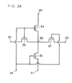
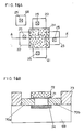
- Fig. 1(a) is a plan view of a semiconductor device according to a first embodiment of the invention.
- a diffusion layer is formed of a pair of a first source 20 and a first drain 21, and a pair of a second source 22 and a second drain 23.
- a common gate 24 is formed in the region between the first source 20, first drain 21, second source 22 and second drain 23.
- contact holes 25 are formed on the diffusion layer of the first source 20 and first drain 21, and the- diffusion layer of the second source 22 and second drain 23. Besides, the contact hole 25 of the common gate 24 is disposed in a region not contacting electrically with the- other diffusion layers.
- the line linking the first source 20 and first drain 21 and the line linking the second source 22 and second source 23 intersect nearly at a right angle.
- the channel width (indicated by "a” in Fig. 1(a)) formed between the first source 20, first drain 21, and the second source 22, second drain 23 is set specific at about 10 ⁇ m.
- the channel length (“b" in Fig. 1(a)) formed between the second source 22 and second drain 23 is about 12 ⁇ m.
- the width of the common gate 24 ("c" in Fig. 1(a)) is about 12 ⁇ m. In the illustrated embodiment, the three ends of the square of the common gate 24 are notched, but such notching is not particularly required.
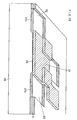
- Fig. 1(b) is a perspective sectional view of the device as seen from line A-A′ in Fig. 1(a), but the contact holes 25 are not shown here.
- a diffusion layer 27a of the second source 22 and a diffusion layer 27b of the second drain 23 are formed, and a gate oxide film 28 is formed between the two diffusion layers 27a, 27b, and a common gate 24 is formed on the gate oxide film 28.
- the sectional structure of the device in the first embodiment is exactly the same as that of the conventional MOS type device.
- a (100)P-type silicon substrate (resistivity 8 to 12 ohm-cm) is used, and by implanting boron ions to the first source 20, first drain 21, second source 22 and second drain 23, P-type diffusion layers 27a, 27b, 29a, 29b are formed, corresponding to the second source 22, second drain 23, first source 20, and first drain 21, respectively.
- the diffusion layers 29a, 29b are not shown in Fig. 1(b).
- the gate oxide film 28 is formed in a thickness of about 20 nm by steam oxidation.
- the common gate 24 is made of polysilicon formed by CVD.
- the other regions on the substrate 26 than the areas for composing the contact holes 25 and common gate 24 are coated with an insulation film 31.
- the device of the invention with the conventional MOS type device, an example of forming the device by using a single crystal silicon substrate 26 is described, but it is not necessary to use a single crystal substrate, and other substrates may be used such as polycrystalline substrate or film, amorphous substrate or film, and others on which diffusion layers to be used as source and drain may be formed, for example, compound substrates, SOI (silicon-on-insulator) and SOS (silicon-on-sapphire). Needless to say, meanwhile, instead of the embodiment of N-channel type device using the P-type silicon substrate, the invention may be also applied to a P-channel type as well.
- SOI silicon-on-insulator
- SOS silicon-on-sapphire
- the channel width "a" formed between the first, second sources 20, 22 and first, second drains 21, 23 is about 10 ⁇ m, and the channel length "b" is 12 ⁇ m, but the dimensions are not limited as far as a conventional MOS type device can operate, and a normal operation is guaranteed if the channel width "a" and channel length "b" are about 1.0 ⁇ m or more.
- FIG. 2(a) is a sectional view of the device in line A-A′ in Fig. 1(a) and the internal physical operation of the device is described referring to Fig. 2(a).
- Fig. 2(a) shows a floating state of the first source 20 and first drain 21 by applying a specific potential between the second source 22 and second drain 23 and applying a specific voltage to the common gate 24.
- the diffusion layer 27a of the second source 22, the diffusion layer 27b of the second drain 23, the gate oxide film 28, and the common gate 24 are identical with those shown in Figs. 1(a), 1(b).
- a depletion layer 32 is formed at the junction of the P-type diffusion layers 27a, 27b and the substrate 26.
- Fig. 2(b) shows a state which operating potentials are applied to the diffusion layers 27a, 27b and common gate 24.
- a specified potential e.g. 1.0 V
- second drain 23 since the potential of the common gate 24 is higher than the threshold voltage of the transistor, a channel 33 called an inverted layer is formed on the surface of the silicon substrate 26 immediately beneath the gate oxide film 28.
- the channel 33 is connected to the diffusion layer 27a and diffusion layer 27b.
- the electrons generated in the diffusion layer 27a move to the diffusion layer 27b through the channel 33 by the electric field generated between the source diffusion layer 27a and drain diffusion layer 27b, and therefore an electric current flows. This action is exactly the same as that of a conventional MOS type device.
- the depletion layer 32 formed in the periphery of the junction between the second drain 23 and the silicon substrate 26 spreads widely. As the depletion layer 32 is spread, the channel 33 formed immediately beneath the gate oxide film 28 can no longer reach the diffusion layer 27b of the second drain 23 (pinch-off), and the current does not increase even if the drain voltage is further raised, thereby reaching the saturated state.
- the channel 33 formed immediately beneath the common gate 24 changes complicatedly corresponding to the potential of the second source 22 and second drain 23 and the potential of the first source 20 and first drain 21.
- the drain current of the device may be intentionally increased or decreased.
- the intrinsic characteristic may be varied, and the state of instability or drift in operation may be intentionally created.
- Fig. 3(a) shows an equivalent circuit of the device of Fig. 1(a).
- MOS type transistors 34, 35 are connected in series.
- MOS type transistors 36, 37 are connected in series.
- the gates of these four MOS type transistors 34, 35, 36, 37 are common gate 24.
- the sources and drains of the MOS type transistors 34, 35, 36, 37 are connected at one point 38.
- a MOS type transistor 41 is formed between the first source 20 and first drain 21, and a MOS type transistor 42 between the second source 22 and second drain 23. Between the first source 20 and second drain 23, a MOS type transistor 43 is formed. Between the second drain 23 and first drain 21, a MOS type transistor 44 is formed, and between the first drain 21 and second source 22, a MOS type transistor 45 is formed. Furthermore, between the second source 22 and first source 20, a MOS type transistor 46 is formed. These MOS type transistor 43 to 46 share a common gate 24.
- the operation of thus composed circuit is explained below.
- the operating potential applied to the second source 22 and second drain 23 acts as a disturbance factor to cause instability or drift in the device characteristic of the device having the first source 20 and first drain 21 as source and drain, respectively.
- the second source 22 and second drain 23 are in floating state, this device acts exactly the same as the conventional MOS type device. That is, a potential is applied to the common gate 24, and a channel is generated immediately beneath the common gate 24. Sequentially, depending on the potential applied to the first source 20 and first drain 21, a current flows in the channel area and the MOS type device operates.
- Fig. 4(a) shows the flow of current occurring when the second source 22 and second drain 23 are grounded.
- the source, drain and gate have the same composition as shown in Fig. 1(a).
- the shaded area in Fig. 4(a) shows the generation region of the channel 33 beneath the gate electrode when a voltage over the threshold voltage is applied to the common gate 24.
- the arrows 1, 2, 3 in the shaded area indicate the flow direction of the current passing through the channel.
- the drain current flows in the direction of arrow 1.
- the second source 22 and second drain 23 are grounded, the three MOS type transistors operate simultaneously. That is, the MOS type transistor having the first source 20 as the source and the first drain 21 as the drain (in Fig.
- the MOS type transistor 41 corresponds to such transistor, and the flow of the current in Fig. 4 (a) corresponds to the direction of arrow 1), the MOS type transistor having the second source 22 as the source and the first drain 21 as the drain (in Fig. 3(b), the MOS type transistor 45 corresponds to such transistor, and the flow of the current in Fig. 4(a) corresponds to the direction of arrow 2), and the MOS type transistor having the second drain 23 as the source and the first drain 21 as the drain (in Fig. 3(b), the MOS type transistor 44 corresponds to such transistor, and the flow of the current in Fig. 4(a) corresponds to the direction of arrow 3) compose a device comprising one drain and three sources.
- the drain current is merely obtained by the sum of the drain currents flowing through the transistors 41, 44, 45.
- the drain current obtained in the device of this embodiment varies the characteristic by affecting mutually more than in the case of the conventional MOS type element possessing common gate.
- the first source 20, the second source 22 and the second drain 23 are all grounded and are at same potential.
- a specific potential is applied only to the first drain 21, and therefore there is no potential difference between the first source 20 and second source 22, and between the first source 20 and second drain 23, and the elements formed between them do not operate.
- the potential it is not required that the potential be identical between the first source 20 and second source 22, and the first drain 21 and second drain 23, and hence the first source 20, first drain 21, second source 22 and second drain 23 may be fixed at different potentials, individually.
- Fig. 4(b) it may be possible to assume an equivalent circuit having the MOS type transistor disposed between the terminals.
- the drain current increases as the gate voltage and drain voltage raise. This characteristic is fundamentally the same as the general MOS type transistor.
- the drain voltage-drain current characteristic was examined when two out of four terminals of the device shown in Fig. 1(a) are floating.
- the terminals are not called by the names of source and drain. This is because the terminals may become either source or drain depending on the applied potential.
- the first source 20 is terminal T1
- the first drain 21 is terminal T3
- the second source 22 is terminal T2
- the second drain 23 is terminal T4.
- the relation between the drain-source voltage and the drain current (referred to as broken line A) of the device having terminals T3 and T4 in floating state was examined using the terminal T2 as the drain for applying a potential of 0 to 5 V and terminal T1 as the source with the potential set at 0 V. At this time, the potential of the common gate 24 varies from 0 to 5 V.
- the two terminals corresponding to the source and drain are disposed at right angle. Accordingly, the channel region is bent almost at right angle and the drain current flowing between the vertically arranged source and drain can be measured
- solid line B examined the variation of the potential from 0 to 5 V in which all potentials of the terminals T2 and T4 are in floating state, the potential of terminal T1 is 0 V, and the terminal T3 is the drain. The potential applied to the common gate 24 is changed from 0 to 5 V.
- the two terminals corresponding to the source and drain are disposed linearly. Accordingly, the channel region is rectangular, same as in the ordinary MOS type transistor.
- the drain current of the MOS type element is inversely proportional to the channel length and normally proportional to the channel width as shown in formula (1).
- the drain current flowing in the device may be intentionally increased or decreased. Accordingly, assuming one of the plurality of sources and drains to be a control terminal of the device possessing other pair of source and drain, by applying an appropriate potential to the control terminal, the intrinsic characteristic of the device may be changed, so that the state of instability or drift in operation may be intentionally created.
- gate voltage and drain current were measured when a voltage is applied to the three terminals. A potential of 0 V was applied to terminal T1, 0.1 V to terminal T3, 0 V to terminal T4 and 0 V ot the substrate. The potential of terminal T2 is varied in a range of 0 to 5 V, and the gate potential is varied in a range of 0 to 2 V.
- This device is regarded as a MOS type transistor having the terminals T1 and T4 as the source and the terminal T3 as the drain.
- the threshold voltage of thus formed MOS type transistor is about 0.7 V, and hence the drain current flowing from terminal T3 begins to flow at the gate potential of 0.7 V or more.
- the drain current flowing from the terminal T3 gradually decreases and finally begins to flow in the reverse direction.
- the MOS type transistor having the terminal T2 as the drain begins to operate, in addition to the drain current of the terminal T3 flowing in the MOS type transistor having the terminals T1 and T4 as the source which had been operating so far. That is, in order to cause the terminals of the MOS type device to operate as the source or drain, it merely depends on which terminal has a higher potential. Therefore, if the potential of the terminal T2 is 0 V, the terminal T3 which is the drain is known to change to the source from around the point where the potential of the terminal T2 is about to exceed 0.1 V. What should be noted here is that the drain current is flowing in the terminal T2 even if the potential of the terminal T2 is 5 V and the potential of the gate is about 0.8 V.
- the threshold voltage of the MOS type device having the first operating terminal T2 as the drain is about 0.8 V.
- the potential of the source which is the terminal T2 of the second operating MOS type element is 0.1 V higher than that of the substrate.
- the original characteristic of the MOS type device may be varied.
- the intrinsic characteristic of the device may be varied, and the state of instability of drift may be intentionally created.
- Fig. 5 shows the result of measurement of gate voltage and drain current in order to show that the apparent threshold voltage can be changed.
- the potential of the terminal T1 is 0 V
- the terminal T2 is opened
- the potential of terminal T3 is 0.1 V
- the potential of the terminal T4 is fixed at 0 V.
- the gate potential is changed in a range of 0 to 2 V
- the diagram shows the gate voltage dependence of the drain current flowing in the terminal T3 when 0 V is applied to the substrate.
- the MOS type transistor is composed by using the terminals T1 and T4 as the source and T3 as drain.
- the potential of the terminal T2 is an intermediate value of the potential of the source and drain.
- the drain current flowing in the terminal T3 decreases.
- the terminal T2 acts as the drain, and the terminal T3 changes its role from drain to source.
- the characteristic is revised to have the threshold voltage about 0.05 V larger. The drain current flowing in terminal T3 at this time decreases about 50%.
- Fig. 6 shows an element having the middle portion cut out from the common gate 24 in the device shown in Fig. 1(a).
- the middle portion of the common gate 24 of the first source 20, first drain 21, second source 22, second drain 23 is cut out, so that the potential induced in the diffusion layer 50 in the middle portion can be taken out independently of the potential applied to other terminals.
- the device shown in Fig. 6 exactly corresponds to the equivalent circuit of the device shown in Fig. 3(a).
- the potential of the diffusion layer 50 in the center portion of the common gate 24 is an intermediate value of 0 and 3 V (this value is called Vc hereinafter). That is, a MOS type transistor using the first source 20 as the source, the diffusion layer 50 as the drain, and applying Vc to the drain, and a MOS type transistor using the diffusion layer 50 as the source, the first drain 21 as the drain, and apply a potential of Vc to the source and 3 V to the drain are arranged in series. The circuit diagram in this state is shown in Fig. 7(a).
- Fig. 7(b) shows a circuit diagram in a state of grounding the second source 22 and second drain 23.
- the potential of the diffusion layer 50 is lowered from the potential Vc by ⁇ Vc to be Vc - ⁇ Vc.
- the drain current flowing in the MOS type transistor 34 in Fig. 7(b) decreases by ⁇ ID.
- the three MOS type transistors 34, 36, 37 have substantially identical size, and hence a nearly equal drain current flows in the three MOS type transistors 34, 36, 37. Accordingly, the total drain current is 3 x (ID - ⁇ ID), and the total drain current increases.
- the difference between the device shown in Fig. 1(a) and the device having the structure shown in Fig. 6 is that the size of the device in Fig. 1(a) determined by the channel length and channel width varies with the condition of the potential applied to the terminals, while the device shown in Fig. 6 does not have four MOS type elements of nearly same channel length and channel width in a symmetrical element because the channel is formed only immediately beneath the common gate. Accordingly, the size of the device is determined when the device is formed in the substrate. Depending on the condition of the potential applied to the terminals, the potential of the diffusion layer 50 varies, and the operation of the entire circuit, formed by four MOS type transistors, changes. That is, in the device shown in Fig.
- the device shown in Fig. 1(a) since the channel region is shared by plural MOS type transistors, according to the operation of one MOS type transistor, the effective channel length and channel width of other MOS type transistors are changed. Therefore, in the element shown in Fig. 1(a), rather than the circuit shown in Fig. 6, the terminals are connected with each other. Besides, from the aspect of formation of device, the device shown in Fig. 1(a) is more advantageous than the device shown in Fig. 6 because it is not necessary to form a gate for forming the diffusion layer 50, so that the device may be designed in a more delicate dimension and in more complicated shape.
- the device shown in Fig. 1(a) is different from the device shown in Fig. 6 because the channel region of the MOS type transistor is shared. Therefore, the drain current is determined by a more complicated mechanism. Having plural pairs of source and drain, by varying the value of the potential applied to each source and drain, the drain current flowing in each transistor may be intentionally increased or decreased. Therefore, assuming one of the plural sources and drains to be a control terminal of the device having an other pair of source and drain, by applying a proper potential to the control terminal, the intrinsic characteristic of the device may be varied.
- Fig. 8 shows a first embodiment of the invention, which has a modified structure of the device shown in Fig. 1(a).
- a diffusion layer of a set of first source 20 and first drain 21, and a set of second source 22 and second drain 23 is formed.
- the first drain 21 and second drain 23 in Fig. 1(a) are connected with a common P-type diffusion layer.
- the first drain 21 and second drain 23 are collectively called the first drain 21.
- a common gate 24 is formed in the region to become the gate of the diffusion layer of the first source 20 and first drain 21 and the diffusion layer of the second source 22 and first drain 21.
- contact holes 25 are formed in the diffusion layer of the first source 20 and first drain 21, and the diffusion layer of the second source 22 and second drain 23.
- a contact hole 25 of the common gate 24 is formed in a region not electrically contacting with other diffusion regions.
- a characteristic feature of the element shown in Fig. 8 is that the device characteristic of specific source and drain is varied by applying a specific voltage to other source and drain terminals.
- the drain is used commonly, at least only one other terminal is sufficient. Therefore, the desired function may be achieved in a structure having at least three source and drain terminals.
- FIG. 9(a) As a second example of the device having a modified structure of the element shown in Fig. 1(a), an embodiment of device having three terminals each is shown in Fig 9(a). Its equivalent circuit is as shown in Figs. 9(b), 9(c).
- numerals 51, 52, 53 are source or drain terminals.
- the width of the three terminals 51, 52, 53 is equal, it is formed in an equilateral triangle.
- a common gate 54 is formed in the region enclosed by the terminals.
- contact holes 55 are formed in the terminals 51, 52, 53 and common gate 54, and a potential may be applied to the terminals 51, 52, 53 and common gate 54 through these contact holes 55 at the time of operation of the device.
- any triangle may be formed by varying the width of the terminals.
- the channel length tends to be longer as compared with the channel width, and it is inferior to the characteristic of the MOS type device.
- the terminals corresponding to the source and drain are symmetrical. That is, the device characteristic is not changed at all if the first source 20 and second source 22, or the first drain 21 and second drain 23 are exchanged with each other. Accordingly, about the middle of the common gate 54, by rotating 90 degrees in Fig. 1(a) or 120 degrees in Fig. 9(a), even if operated by applying the above potential to the terminals, the same device characteristic is obtained.
- the terminals by symmetrical. That is, by applying a potential to a specific terminal, the function of controlling the current flowing in other terminals is achieved also by an asymmetrical structure not allowing to exchange the terminals. Therefore, the manner of operation of individual source terminals, drain terminals and control terminals may be fixed.
- Figs. 10(a), (b), (c) refer to embodiments composed so as to control the drain current flowing in a specific MOS type element by making common the channels of the other device, with respect to the channel of the specific MOS type device.
- the width of the channel region formed between the first source 20 and first drain 21 is set about 10 to 20 times larger than the width of the channel region formed between the second source 22 and second drain 23.
- the drain current flowing in the specific MOS type device can be changed by only about 5 to 10%. That is, in this range, the characteristic of the specific MOS type device can be varied only very slightly by the potential applied from outside.
- Fig. 10(a) there are two other control terminals, the second source 22 and second drain 23, with respect to the specific MOS type transistor possessing the first source 20 and first drain 21.
- Fig. 11 shows the relation between the drain potential and drain current of the device shown in Fig. 10(c).
- a potential of 0 V is applied to the first source 20 and substrate, and a potential of 5 V to the common gate 24.
- Potentials of 0 V and 2 V are applied to the second drain 23 to be used as parameters.
- a potential in a range of 0 to 5 V is applied to the first drain 21 to the first drain 21 to the first drain 21 to the first drain 21, a potential in a range of 0 to 5 V is applied.
- the device structure shown in Fig. 10(c) is to add a second drain 23 as control terminal to the ordinary MOS type transistor with the channel width of 20 ⁇ m and channel length of 2 ⁇ m.
- the added MOS type transistor has the channel length of about 2 ⁇ m and channel width of about 1 ⁇ m, and the drain current flowing at this time is about 1/20 of the usual current.
- potentials of 0 V, 2 V are applied to the second drain 23 which is the control terminal, it is known that the flowing drain current fluctuates about 5%. Therefore, by applying an arbitrary potential to the control terminal from outside, it is known that the characteristic of the specific MOS type transistor is changed.
- the electric characteristic of the ordinary MOS type transistor is determined when forming the element as described herein. Accordingly the control is effected to satisfy the specific standard, but it is judged whether the standard is satisfied or not only by the evaluation after formation of the device.
- the device is experimentally formed to collect the data of the device characteristic, and the data is fed back to the design to form a desired circuit.
- the electric characteristic of the device can be modified after forming the device, it is possible to control so as to present the device characteristic of the highest performance.
- the circuit is composed so as to change the device characteristic after the formation of the device, it is not required to replace all devices with the devices shown in Fig. 10(c), and only specific devices largely affecting the circuit characteristic may be modified.
- the potential to be applied to the control terminal of the replaced device may be fixed at a specific external potential through an output terminal, or the potential may be applied to the control terminal through feedback loop so as to be adjusted by self-matching.
- the element with excellent performance may be formed at a high yield, and optimization of the circuit operation or data collection in designing of circuit may be done easily.
- the majority of the channel region overlaps with four MOS type tansistors. Accordingly, the drain current flowing in each MOS type transistor is exposed to the effect to the maximum effect by the potential applied to the transistors.
- the degree of such effect may be varied arbitrarily. That is, by reducing the overlap of the channel region, the mutual effect may be decreased.
- a first source 55 is common, and in order to reduce the overlap of the channels formed by each pair of drain and source, four drains (first drain 56, second drain 57, third drain 58, fourth drain 59) are disposed parallel to each other. Furthermore, a common gate 60 is formed in the region enclosed by the first source 55 and the four drains 56 to 59. In addition, contact holes 61 are formed in the first source 55, four drains 56 to 59, and common gate 60.
- the rate of the drain current influenced by the potential applied to other drain terminals is about 20% only.
- the degree of mutually affecting with other drain terminals may be arbitrarily set.
- the devices shown in Fig. 1(a) and Fig. 9(a) can possess characteristics that cannot be obtained in the device formed merely by combining the conventional MOS type transistors.
- the drain current flowing in the specific MOS type transistor varies, and this characteristics is convenient for composing a circuit of complicated and mutual connections such as the neuron (nerve circuit).
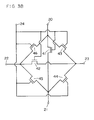
- Fig. 13 shows an embodiment of a circuit composed by using the devices shown in Fig. 1(a).
- the device shown in Fig. 13 is indicated by the o mark, and the x mark in the o mark refers to the four straight lines seen from the center of the x, corresponding respectively to the first source 20, first drain 21, second source 22 and second drain 23.
- the straight line above and below the o mark indicates the common gate 24.
- the x mark in the o mark refers to the four straight lines seen from the center of the x, corresponding respectively to the first source 20, first drain 21, second source 22 and second drain 23.
- the straight line above and below the o mark indicates the common gate 24.
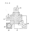
- the gate 41 devices in this example, are arranged in a matrix, and the gate is common in the vertical direction, and the gate terminals are as many as the number of rows of arrangement, or nine gate terminals 65 in this example.
- Each element forms a part of an input terminal 66 and a part of an output terminal 67 by mutually connecting the first source 20 and first drain 21.
- each element forms a part of an input terminal 66 and a part of an
- An electric signal applied to an input terminal 66 is converted on the matrix shown in Fig. 13 , and is delivered to an output terminal 67. All outputs are affected by the electric signals from the input terminals 66, and therefore one output may include all input information, and therefore the data is holographic (multiplex).
- a character or image may be recognized by the information read in through the image scanner. Such processing is required in order to judge if identical or not even when the reading position is deviated or the contrast difference is absorbed because the relation of contrast of adjacent pieces of information is important.
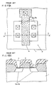
- a structure of junction type field effect transistor is shown in Fig. 14.
- Fig. 14(a) is a plan view of JFET. As far as the plan view is concerned, there is nothing different from the plan view of the device shown in Fig. 1(a).
- the source and drain of the JFET are composed of impurities of the same conductive type. Diffusion layers of a set of first source 20 and first drain 21 and a set of second source 22 and second drain 23 are formed.
- a common gate 24 is formed in the region of the gate of the diffusion layer of first source 20 and first drain 21 and the gate of the diffusion layer of second source 22 and second drain 23.
- contact holes 25 are formed in the diffusion layer of first source 20 and first drain 21, and the diffusion layer of second source 22 and second drain 23.
- a contact hole 25 of the common gate 24 is formed in a region not contacting electrically with the other diffusion layers.
- the line linking the first source 20 and first drain 21, and the line linking the second source 22 and second drain 23 are intersecting almost at right angle. There is also a region 68 for applying a substrate voltage.
- Fig. 14(b) is a sectional view of the element in line A-A' shown in Fig. 14(a) during operation of JFET.
- a diffusion layer 70a to be the second source 22 and a diffusion layer 70b to be the second drain 23 are formed in the silicon substrate 69.
- a gate oxide film 71 is formed on the silicon substrate 69 on the second source 22 and second drain 23.
- a gate electrode 72 made of polysilicon is formed on the gate oxide film 71.
- the diffusion layer 70a and diffusion layer 70b are connected, and a channel 74 is formed at a deep position inside the substrate immediately beneath the gate.
- the drain current flowing in a specific transistor may be controlled by varying the potential applied to other transistors.
- the drain current flowing in the transistor may be intentionally increased or decreased.
- the devices of high performance may be formed at high yield, and the optimization of the circuit operation and data collection in designing of circuit may be achieved easily.
- the hitherto impossible device characteristics may be realized. That is, having plural pairs of source and drain, by varying the value of the potential applied to each source and drain, the drain current flowing in the device may be intentionally increased or decreased.
- the intrinsic characteristic of the device may be varied, and the state of instability of drift in operation may be intentionally created.
- a desired circuit may be composed easily in the circuit design.
- the hitherto impossible circuit may be composed.
- the electric characteristic of the device may be varied after forming a device or a circuit, it may be possible to cause characteristics of the highest performance. Since the device characteristics can be freely varied, the devices of superb performance may be formed at high yield, and optimization of circuit operation and data collection in circuit design may be achieved easily.
Landscapes
- Metal-Oxide And Bipolar Metal-Oxide Semiconductor Integrated Circuits (AREA)
- Junction Field-Effect Transistors (AREA)
- Insulated Gate Type Field-Effect Transistor (AREA)
Claims (7)
- Dispositif de transistor à effet de champ comprenant :(a) un substrat semiconducteur (26) ;(b) des première et seconde couches de diffusion (27a, 27b) formées dans ledit substrat semiconducteur ;(c) une troisième couche de diffusion jouant le rôle de borne de commande, ladite troisième couche de diffusion étant formée en une position indépendante desdites première et seconde couches de diffusion (27a, 27b) dans ledit substrat semiconducteur ; et(d) une grille commune (24), lesdites première, seconde et troisième couches de diffusion étant formées de façon externe autour de ladite grille commune,dans lequel une unique région de canal (33) est formée au-dessous de la grille et entre les couches de diffusion.
- Dispositif à semiconducteur selon la revendication 1, dans lequel ledit canal (33) est formé dans la région de surface dudit substrat semiconducteur (26).
- Dispositif à semiconducteur selon la revendication 1, dans lequel ledit canal (33) est formé à l'intérieur dudit substrat semiconducteur (26).
- Dispositif à semiconducteur selon la revendication 1, dans lequel ladite troisième couche de diffusion est formée sur une ligne pratiquement orthogonale à la ligne reliant lesdites première et seconde couches de diffusion (27a, 27b).
- Dispositif à semiconducteur selon la revendication 1, dans lequel la forme dudit canal (33) est triangulaire.
- Dispositif à semiconducteur selon l'une quelconque des revendications précédentes, dans lequel une quatrième couche de diffusion est formée dans le substrat semiconducteur, lesdites couches de diffusion étant agencées en tant que deux paires de couches de diffusion, chaque paire comportant ladite grille commune entre.
- Dispositif à semiconducteur selon la revendication 6, dans lequel une couche de diffusion d'une desdites paires est formée selon une connexion commune avec une couche de diffusion de l'autre desdites paires.
Applications Claiming Priority (2)
| Application Number | Priority Date | Filing Date | Title |
|---|---|---|---|
| JP15342589 | 1989-06-15 | ||
| JP153425/89 | 1989-06-15 |
Publications (3)
| Publication Number | Publication Date |
|---|---|
| EP0403267A2 EP0403267A2 (fr) | 1990-12-19 |
| EP0403267A3 EP0403267A3 (fr) | 1991-06-26 |
| EP0403267B1 true EP0403267B1 (fr) | 1996-11-27 |
Family
ID=15562230
Family Applications (1)
| Application Number | Title | Priority Date | Filing Date |
|---|---|---|---|
| EP90306462A Expired - Lifetime EP0403267B1 (fr) | 1989-06-15 | 1990-06-13 | Dispositif semi-conducteur |
Country Status (3)
| Country | Link |
|---|---|
| EP (1) | EP0403267B1 (fr) |
| JP (1) | JP2633376B2 (fr) |
| DE (1) | DE69029226T2 (fr) |
Families Citing this family (8)
| Publication number | Priority date | Publication date | Assignee | Title |
|---|---|---|---|---|
| JPH0814702A (ja) * | 1994-06-27 | 1996-01-19 | Nippondenso Co Ltd | 積層型蒸発器 |
| US5806054A (en) * | 1997-02-14 | 1998-09-08 | National Semiconductor Corporation | Neuron MOSFET module structure for binary logic circuits |
| JP4202012B2 (ja) | 2001-11-09 | 2008-12-24 | 株式会社半導体エネルギー研究所 | 発光装置及び電流記憶回路 |
| FR2883168B1 (fr) | 2005-03-18 | 2008-01-11 | Oreal | Compositions cosmetiques de soin, renforcement et/ou reparation des substrats keratiniques comprenant des polypeptides kap |
| JP5063539B2 (ja) * | 2008-09-12 | 2012-10-31 | 株式会社半導体エネルギー研究所 | 半導体装置及びそれを用いたモジュール、電気器具 |
| JP4796635B2 (ja) * | 2009-01-22 | 2011-10-19 | 株式会社沖データ | 駆動回路、光プリントヘッド及び画像形成装置 |
| JP5526108B2 (ja) * | 2011-11-14 | 2014-06-18 | 株式会社半導体エネルギー研究所 | 発光装置 |
| JP7421532B2 (ja) * | 2021-11-12 | 2024-01-24 | キヤノン株式会社 | 光電変換装置及び発光装置 |
Family Cites Families (3)
| Publication number | Priority date | Publication date | Assignee | Title |
|---|---|---|---|---|
| JPS6072257A (ja) * | 1983-09-28 | 1985-04-24 | Nec Corp | 半導体集積回路 |
| JPS61290767A (ja) * | 1985-06-19 | 1986-12-20 | Hitachi Ltd | Mos電界効果トランジスタ |
| JPH0770613B2 (ja) * | 1988-02-29 | 1995-07-31 | 日本電気株式会社 | 半導体集積回路の製造方法 |
-
1990
- 1990-06-13 EP EP90306462A patent/EP0403267B1/fr not_active Expired - Lifetime
- 1990-06-13 DE DE69029226T patent/DE69029226T2/de not_active Expired - Fee Related
- 1990-06-15 JP JP2157997A patent/JP2633376B2/ja not_active Expired - Lifetime
Also Published As
| Publication number | Publication date |
|---|---|
| DE69029226T2 (de) | 1997-05-15 |
| DE69029226D1 (de) | 1997-01-09 |
| EP0403267A2 (fr) | 1990-12-19 |
| JP2633376B2 (ja) | 1997-07-23 |
| JPH0387071A (ja) | 1991-04-11 |
| EP0403267A3 (fr) | 1991-06-26 |
Similar Documents
| Publication | Publication Date | Title |
|---|---|---|
| US5331192A (en) | Semiconductor device | |
| KR100220608B1 (ko) | 반도체 장치 | |
| EP0469611A1 (fr) | Dispositif à semi-conducteur à injection tunnel et son procédé de fabrication | |
| KR890003147B1 (ko) | 게이트 에레이 | |
| EP0348998B1 (fr) | Circuit integré semi-conducteur comportant un circuit différentiel à transistors comprenant une paire de FET's | |
| JP3367776B2 (ja) | 半導体装置 | |
| US4908682A (en) | Power MOSFET having a current sensing element of high accuracy | |
| DE102010028275A1 (de) | Integrierter Seebeck-Differenztemperatursensor | |
| EP0403267B1 (fr) | Dispositif semi-conducteur | |
| EP0593865B1 (fr) | Dispositif de mémoire à semi-conducteur et procédé de fabrication | |
| US6198140B1 (en) | Semiconductor device including several transistors and method of manufacturing the same | |
| US5258625A (en) | Interband single-electron tunnel transistor and integrated circuit | |
| US4969020A (en) | Semiconductor device | |
| JPH0419711B2 (fr) | ||
| KR100229859B1 (ko) | 반도체 장치 | |
| US6184588B1 (en) | SRAM cell having bit line shorter than word line | |
| JPH0324070B2 (fr) | ||
| USRE38647E1 (en) | Sense amplifier circuit | |
| KR19980069994A (ko) | 반도체 장치 및 그 제조 방법 | |
| US7193275B2 (en) | Semiconductor device allowing modulation of a gain coefficient and a logic circuit provided with the same | |
| US6153915A (en) | CMOS semiconductor device | |
| US5311463A (en) | Semiconductor memory device and manufacturing method thereof | |
| JPH04118964A (ja) | 薄膜トランジスタ | |
| JP3059607B2 (ja) | 半導体記憶装置およびその製造方法 | |
| KR100203604B1 (ko) | 판독된 선택 트랜지스터를 구비한 비휘발성 반도체 메모리 |
Legal Events
| Date | Code | Title | Description |
|---|---|---|---|
| PUAI | Public reference made under article 153(3) epc to a published international application that has entered the european phase |
Free format text: ORIGINAL CODE: 0009012 |
|
| AK | Designated contracting states |
Kind code of ref document: A2 Designated state(s): DE FR GB NL |
|
| PUAL | Search report despatched |
Free format text: ORIGINAL CODE: 0009013 |
|
| AK | Designated contracting states |
Kind code of ref document: A3 Designated state(s): DE FR GB NL |
|
| 17P | Request for examination filed |
Effective date: 19911223 |
|
| 17Q | First examination report despatched |
Effective date: 19931029 |
|
| GRAG | Despatch of communication of intention to grant |
Free format text: ORIGINAL CODE: EPIDOS AGRA |
|
| GRAH | Despatch of communication of intention to grant a patent |
Free format text: ORIGINAL CODE: EPIDOS IGRA |
|
| GRAH | Despatch of communication of intention to grant a patent |
Free format text: ORIGINAL CODE: EPIDOS IGRA |
|
| GRAA | (expected) grant |
Free format text: ORIGINAL CODE: 0009210 |
|
| AK | Designated contracting states |
Kind code of ref document: B1 Designated state(s): DE FR GB NL |
|
| REF | Corresponds to: |
Ref document number: 69029226 Country of ref document: DE Date of ref document: 19970109 |
|
| ET | Fr: translation filed | ||
| PGFP | Annual fee paid to national office [announced via postgrant information from national office to epo] |
Ref country code: GB Payment date: 19970604 Year of fee payment: 8 |
|
| PGFP | Annual fee paid to national office [announced via postgrant information from national office to epo] |
Ref country code: FR Payment date: 19970610 Year of fee payment: 8 |
|
| PGFP | Annual fee paid to national office [announced via postgrant information from national office to epo] |
Ref country code: DE Payment date: 19970620 Year of fee payment: 8 |
|
| PGFP | Annual fee paid to national office [announced via postgrant information from national office to epo] |
Ref country code: NL Payment date: 19970630 Year of fee payment: 8 |
|
| PLBE | No opposition filed within time limit |
Free format text: ORIGINAL CODE: 0009261 |
|
| STAA | Information on the status of an ep patent application or granted ep patent |
Free format text: STATUS: NO OPPOSITION FILED WITHIN TIME LIMIT |
|
| 26N | No opposition filed | ||
| PG25 | Lapsed in a contracting state [announced via postgrant information from national office to epo] |
Ref country code: GB Free format text: LAPSE BECAUSE OF NON-PAYMENT OF DUE FEES Effective date: 19980613 |
|
| PG25 | Lapsed in a contracting state [announced via postgrant information from national office to epo] |
Ref country code: NL Free format text: LAPSE BECAUSE OF NON-PAYMENT OF DUE FEES Effective date: 19990101 |
|
| GBPC | Gb: european patent ceased through non-payment of renewal fee |
Effective date: 19980613 |
|
| PG25 | Lapsed in a contracting state [announced via postgrant information from national office to epo] |
Ref country code: FR Free format text: LAPSE BECAUSE OF NON-PAYMENT OF DUE FEES Effective date: 19990226 |
|
| NLV4 | Nl: lapsed or anulled due to non-payment of the annual fee |
Effective date: 19990101 |
|
| PG25 | Lapsed in a contracting state [announced via postgrant information from national office to epo] |
Ref country code: DE Free format text: LAPSE BECAUSE OF NON-PAYMENT OF DUE FEES Effective date: 19990401 |
|
| REG | Reference to a national code |
Ref country code: FR Ref legal event code: ST |