EP0404191A2 - Schalteinrichtung für Leistungsversorgung - Google Patents
Schalteinrichtung für Leistungsversorgung Download PDFInfo
- Publication number
- EP0404191A2 EP0404191A2 EP90111905A EP90111905A EP0404191A2 EP 0404191 A2 EP0404191 A2 EP 0404191A2 EP 90111905 A EP90111905 A EP 90111905A EP 90111905 A EP90111905 A EP 90111905A EP 0404191 A2 EP0404191 A2 EP 0404191A2
- Authority
- EP
- European Patent Office
- Prior art keywords
- switching
- voltage
- power supply
- supply device
- rectifying
- Prior art date
- Legal status (The legal status is an assumption and is not a legal conclusion. Google has not performed a legal analysis and makes no representation as to the accuracy of the status listed.)
- Granted
Links
Images


Classifications
-
- H—ELECTRICITY
- H02—GENERATION; CONVERSION OR DISTRIBUTION OF ELECTRIC POWER
- H02M—APPARATUS FOR CONVERSION BETWEEN AC AND AC, BETWEEN AC AND DC, OR BETWEEN DC AND DC, AND FOR USE WITH MAINS OR SIMILAR POWER SUPPLY SYSTEMS; CONVERSION OF DC OR AC INPUT POWER INTO SURGE OUTPUT POWER; CONTROL OR REGULATION THEREOF
- H02M3/00—Conversion of DC power input into DC power output
- H02M3/22—Conversion of DC power input into DC power output with intermediate conversion into AC
- H02M3/24—Conversion of DC power input into DC power output with intermediate conversion into AC by static converters
- H02M3/28—Conversion of DC power input into DC power output with intermediate conversion into AC by static converters using discharge tubes with control electrode or semiconductor devices with control electrode to produce the intermediate AC
- H02M3/325—Conversion of DC power input into DC power output with intermediate conversion into AC by static converters using discharge tubes with control electrode or semiconductor devices with control electrode to produce the intermediate AC using devices of a triode or a transistor type requiring continuous application of a control signal
- H02M3/335—Conversion of DC power input into DC power output with intermediate conversion into AC by static converters using discharge tubes with control electrode or semiconductor devices with control electrode to produce the intermediate AC using devices of a triode or a transistor type requiring continuous application of a control signal using semiconductor devices only
- H02M3/33569—Conversion of DC power input into DC power output with intermediate conversion into AC by static converters using discharge tubes with control electrode or semiconductor devices with control electrode to produce the intermediate AC using devices of a triode or a transistor type requiring continuous application of a control signal using semiconductor devices only having several active switching elements
- H02M3/33571—Half-bridge at primary side of an isolation transformer
-
- H—ELECTRICITY
- H02—GENERATION; CONVERSION OR DISTRIBUTION OF ELECTRIC POWER
- H02M—APPARATUS FOR CONVERSION BETWEEN AC AND AC, BETWEEN AC AND DC, OR BETWEEN DC AND DC, AND FOR USE WITH MAINS OR SIMILAR POWER SUPPLY SYSTEMS; CONVERSION OF DC OR AC INPUT POWER INTO SURGE OUTPUT POWER; CONTROL OR REGULATION THEREOF
- H02M3/00—Conversion of DC power input into DC power output
- H02M3/01—Resonant DC/DC converters
Definitions
- the present invention relates to a switching power supply device for supplying a stabilized DC voltage to an industrial or household electronic apparatus.
- a self-excited flyback type switching power supply device has been widely used, because it consists of fewer parts and can be manufactured at a relatively low cost. It is known, however, that the switching frequency of such a device fluctuates depending upon degree of the output current, with the result that interferences occur in the operation of an associated electronic apparatus and that a larger size rectifying and smoothing circuit is required.
- Figure 7 shows a switching power supply device of such at type.
- the device of Figure 7 comprises a DC power source 1, a transformer 3, switching elements 4 and 14, a diode 5, a synchronizing oscillation circuit 6, a rectifying diode 7, a smoothing capacitor 8, a secondary switching element 14, and a control circuit 15.
- the DC power source 1 rectifies an AC voltage and smoothes the resulting DC voltage. Alternatively it may consist of a battery or the like.
- the positive and negative terminals of the DC power source 1 are connected to input terminals 2 and 2′, respectively.
- the transformer 3 has: a primary winding 3a connected at one terminal to the input terminal 2 and at the other terminal to the input terminal 2′ through the switching element 4; a secondary winding 3c connected at one terminal to an output terminal 10′ and at the other terminal to an output terminal 10 through the rectifying diode 7; and a bias winding 3b connected at one terminal to the input terminal 2′ and at the other terminal to the synchronizing oscillation circuit 6.
- the switching element 4 turns ON or OFF in response to ON/OFF signals which are supplied at the control terminal from the synchronizing oscillation circuit 6. thereby applying the input voltage to the primary winding 3a and interrupting the voltage.
- the synchronizing oscillation circuit 6 actuates the switching element 4 to turn ON and OFF respectively for predetermined ON and OFF periods of time. The OFF period continues until the polarity of the induced voltage of the bias winding 3b is inverted. This repeated ON/OFF cycle causes continuous oscillation.
- the energy accumulated in the transformer 3 during an ON period of the switching element 4 is released from the secondary winding 3c through the rectifying diode 7 or the switching element 14 to the smoothing capacitor 8 during an OFF period of the switching element 4.
- a secondary current is caused to flow reversely from the smoothing capacitor 8 to the secondary winding 3c through the switching element 14.
- the period of this reverse flow is controlled by the control circuit 15.
- the rectifier diode 7 is connected at its anode to one terminal of the secondary winding 3c and at its cathode to the output terminal 10.
- the smoothing capacitor 8 is connected between the output terminals 10 and 10′.
- the induced voltage appearing across the secondary winding 3c is rectified by the rectifying diode 7, and then smoothed by the smoothing capacitor 8 to provide an output voltage.
- the control circuit 15 compares the voltage appearing across the output terminals 10 and 10′ with an internal reference voltage in order to vary the above-mentioned flow period of the secondary current through the secondary switching element 14.
- FIG. 8 shows the waveform of a voltage V DS appearing across the switching element 4; (b) the primary current I D flowing through the primary winding 3a; (c) the waveform of driving pulse V G1 output from the synchronizing oscillation circuit 6; (d) the secondary current I D flowing through the secondary winding 3c; and (e) the waveform of a driving pulse V G2 for the secondary switching element 14.
- the hatched portions in (e) of Figure 8 indicate reverse flow periods for causing the secondary current I o to reversely flow in the secondary winding 3c.
- a magnetic flux develops in the transformer 3 as the primary current I D flows through the primary winding 3a during an ON period of the switching element 4 which period is determined by the synchronizing oscillation circuit 6, so that energy is accumulated in the transformer 3, whereupon an induced voltage develops in the secondary winding 3c. It is so arranged that the rectifying diode 7 is reversely biased by the induced voltage and that the switching element 14 remains in its OFF-position.
- the switching element 4 turns OFF in response to an OFF signal from the synchronizing oscillation circuit 6, a fly-back voltage develops in the primary winding 3a, and, simultaneously, a fly-back voltage is induced in the secondary winding 3c in such a direction that the rectifying diode 7 is forward biased.
- the energy accumulated in the transformer 3 is released as a secondary current I o through the secondary winding 3c, which is then smoothed by the smoothing capacitor 8 and supplied as an output voltage to the output terminals 10 and 10′.
- the switching element 14 is actuated to turn ON by the control circuit 15, but there occurs no particular operation change, through whichever the diode 7 or the switching element 14 the secondary current may flow.
- the ON period of the switching element 14 is controlled by the control circuit 15.
- the switching element 14 becomes OFF, the induced voltage in each winding of the transformer 3 is inverted in polarity. Therefore, the induced voltage developing in the secondary winding 3c causes the rectifying diode 7 to be reversely biased. Since the switching element 14 is in the OFF state, the secondary winding current does not flow. In the primary winding 3a, the induced voltage develops in such a direction that the voltage at the terminal to which the switching element 4 is connected is negative, and, on the other hand, the voltage at the terminal to which input terminal 2 is connected is positive.
- the primary current flows in such a direction that the DC power source 1 is charged through the diode 5, so that the energy accumulated in the transformer 3 during the OFF period is supplied to the DC power source 1 (i.e., the power regeneration is conducted).
- the polarity of the induced voltage developing in the bias winding 3b is also inverted, and accordingly the synchronizing oscillation circuit 6 actuates the switching element 4 to turn ON. In this case, there is no particular operational change, through whichever the diode 5 or the switching element 4 the primary current may flow.
- N S represents the number of turns of the secondary winding 3c
- N P represents the number of turns o£ the primary winding 3a
- L S represents the inductance of the secondary winding 3c
- V IN represents the input voltage supplied from the DC power source 1.
- the ON period T ON is kept at a constant value determined by the synchronizing oscillation circuit 6. If the output voltage V OUT is constant, therefore, the OFF period T OFF is constant, and the oscillation frequency f is also constant.
- the reverse flow period T′ OFF can be changed by controlling the ON period of the switching element 14 which is controlled by the control circuit 15.
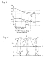
- Figure 9 shows various waveforms obtained when the output current I OUT is changed.
- solid lines indicate waveforms obtained when the output currentI OUT flows at the maximum level from the output terminals 10 add 10′, or at the so-called maximum load period
- broken lines indicate waveforms obtained when the output current I OUT is zero, or at the socalled no-load period.
- the conventional regenerative control type switching power supply device provides an advantage that because of its ability to regenerate energy at the turn ON of the switching element 4, even when a snubbing capacitor is connected between the both terminals of the switching element 4, the surge voltage at the turn-on can be efficiently restrained without involving any turn-on loss.
- the resonance energy due to the capacitor and the leakage inductance of the transformer 3 is considerably great, so that ringing waveforms are superposed over another throughout each OFF period, which becomes a source of noise.
- the addition of a larger snubbing capacitor becomes a greater hindrance to realization of a higher switching frequency for compactness of the power source.
- the rectifying and smoothing circuit is of the capacitor input type which comprise a smoothing element and a capacitor and that the capacitor is used as an input capacitor which serves as a DC power source.
- the output holding time is required to be set in order to protect electronic apparatuses as a load from possible troubles such as momentary interruption of input power.
- the output holding time depends largely upon the static capacitance of the input capacitor, and, therefore, the static capacitance is determined by both the power capacity of the power source and the output holding time.
- the conducting period of the input current from the AC power source is shorter in the stage of steady operation so that the peak value of the input current becomes larger, thereby causing the problem in that the power factor and efficiency substantially drop.
- the switching power supply device comprises a DC power source, and a transformer having at least primary and secondary windings, and further comprises: a first switching means which is connected in series with said primary winding, this series circuit being connected to the terminals of said DC power source; a second switching means; a capacitor which is connected in series with said second switching means, this series circuit being connected to the terminals of said primary winding; a rectifying and smoothing circuit for rectifying and smoothing a flyback voltage which generate in said secondary winding and for outputting a resulting DC voltage; and a drive means for driving alternately said first and second switching means with predetermined ON-OFF periods.
- the switching power supply device may further comprise at least one resonance capacitors which are connected respectively to the terminals of at least one of said first and second switching means and said primary and secondary windings.
- the switching power supply device comprising a transformer having at least primary and secondary windings, and further comprises: a rectifying circuit for receiving and rectifying an AC voltage, said rectifying circuit comprising at least one rectifying element; an input capacitor means for smoothing the output of said rectifying circuit: a first switching means which is connected in series with said primary winding, this series circuit being connected to said input capacitor means; a second switching means; a capacitor which is connected in series with said second switching means, this series circuit being connected to the terminals of said primary winding; a rectifying and smoothing circuit for rectifying and smoothing a flyback voltage which generates in said secondary winding and for outputting a resulting DC voltage; and a drive means for driving alternately said first and second switching means with predetermined ON-OFF periods.
- At least one of said first and second switching means may comprise a switching element and a diode means which are connected in parallel.
- said transformer further has a bias winding
- said driving means comprises: a first control means for driving said first switching means, said first control means being connected to said bias winding; and said and a second control means for driving said second switching means, said second control means being connected to the output terminals.
- the second switching means is ON at that time, the voltage present across the capacitor is applied to the primary winding of the transformer, there being little or no possibility of ringing occurrence.
- the resonance capacitor connected to the switching means or to the both terminals of the switching means resonates with the leakage inductance of the transformer during the turn-on or turn-off operation, thereby lowering the rate of variation of the operating voltage, so that the level of switching noise can be reduced.
- the energy accumulated in the capacitor connected in series with the second switching means to the terminals of the primary winding of the transformer is released from the secondary winding through the transformer during each ON period of the second switching means, and therefore, longer output holding time can be obtained as compared with the prior art arrangement.
- FIG. 1 shows a switching power supply device according to the invention.
- the device of Figure 1 comprises a DC power source 1, a transformer 3, a switching element 4, a diode 5, a rectifying diode 7, a synchronising oscillation circuit 6, a smoothing capacitor 8, and a control circuit q.
- the switching element 4 and the diode 5 are connected in parallel, and constitute the first switching means.
- the switching element 4 is controlled by the synchronizing oscillation circuit 6.
- the rectifying diode 7 and the smoothing capacitor 8 constitute the rectifying and smoothing circuit.
- the transformer 3 comprises a primary winding 3a, a secondary winding 3c, and a bias winding 3b.
- the device of Figure 1 further comprises another switching element 11 which is controlled by the control circuit 9, another diode 12, and a capacitor 13.
- the switching element 11 and the diode 12 are connected in parallel, and constitute the second switching means.
- the control circuit 9 has input portions connected respectively to output terminals 10 and 10′. The input portions of the control circuit 9 are electrically separated from the output portions connected to the switching element 11.
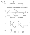
- FIG. 2 shows the waveform of a voltage V DS present across the switching element 4; (b) a primary current I D flowing through the switching element 4 or the diode 5; (c) the waveform of a driving pulse V G1 output from the synchronizing oscillation circuit 6; (d) a primary current I c flowing through the switching element 11 or the diode 12; (e) the waveform of a driving pulse V G2 for the switching element 11; (f) a secondary current I o flowing through the secondary winding 3c; and (g) the variation in the magnetic flux ⁇ of the transformer 3.
- the primary current I D flows through the primary winding 3a during an ON period of the switching element 4 which period is determined by the synchronizing oscillation circuit 6, a magnetic flux develops in the transformer 3 so that energy is accumulated in the transformer 3, whereupon an induced voltage develops in the secondary winding 3c.
- the secondary winding 3c is wound in such a manner that the rectifying diode 7 is reversely biased by this induced voltage. It is so arranged that the diode 12 in the primary side is reversely biased by this induced voltage, and also that the switching element 11 is controlled so as to remain in its OFF-position under this condition.
- the primary current I c is then smoothed by the capacitor 13 to be supplied as a DC voltage V c
- the secondary current I o is smoothed by the smoothing capacitor 8 to be supplied as an output voltage to the output terminals 10 and 10′.
- the switching element 11 is actuated to turn ON by the control circuit 9, but there occurs no particular operation change, through whichever the diode 12 or the switching element 11 the primary current I c may flow.
- the energy accumulated in the transformer 3 begins to be released first from the primary winding 3a under the influence of the leakage inductance, at the voltage reverse in each windings of the transformer 3 caused by the OFF operation of the switching element 4. That is, the primary current I c begins to flow with the initial value which coincides with the final value I p of the primary current current I D , while the secondary current I o rises from zero.
- the magnetic flux ⁇ in the transformer 3 decreases linearly, because the accumulated energy in the transformer 3 is released while the DC voltage V c is applied to the primary winding 3a. Accordingly, the primary current I c decreases monotonously until it is finally reduced to 0 Amp.
- the DC voltage V c remains to be applied by the switching element 11, whereby the transformer 3 is reversely excited and energy is accumulated therein in the inverse direction.
- the switching element 11 is turned OFF by the control circuit 9, the voltages of the windings of the transformer 3 are inverted, and the rectifying diode 7 is reverse-biased, so that the flow of secondary current I o is ceased.
- the induced voltage in the primary winding 3a has a direction such that the polarity at the terminal to which the switching element 4 is connected is negative and the polarity at the terminal to which the input terminal 2 is connected is made positive.
- primary current I D flows through the diode 5 in a direction that the DC power source 1 is charged, whereby the energy accumulated in the transformer 3 during the OFF period is supplied to the DC power source 1 for power regeneration.
- the polarity of the induced voltage developing in the bias winding 3b is also inverted, and, accordingly, the synchronizing oscillation circuit 6 actuates the switching element 4 to turn ON; it is noted, however, that there is no particular change in operation, through whichever the switching element 4 or the diode 5 the primary current I D may flow.
- the switching element 4 operating in ON intervals as determined by the synchronizing oscillation circuit 6 When the switching element 4 operating in ON intervals as determined by the synchronizing oscillation circuit 6 is turned OFF, the energy accumulated in the transformer 3 is released through the primary winding 3a to the capacitor 13, and is also released as the secondary current I o through the secondary winding 3c to the output. Through repetition of cycles of these operations the output voltage is continuously supplied from the output terminals 10 and 10′.
- the DC voltage V c is expressed by the following expression: This becomes when, in the operation for stabilization of the output voltage as already described with respect to the prior art regenerative control type switching power supply device, the DC voltage V c is considered to be a no-load output voltage.
- the output voltage V OUT in the switching power supply device of the embodiment is obtained by rectifying the flyback voltage of the secondary winding 3c
- the following relation is obtained:
- the output voltage V OUT can be regulated by adjusting the DC voltage V c .
- the ON period of the switching element 11 ie., the OFF period T OFF of the switching element 4
- the control circuit 9 so the amount of outgoing charge in the capacitor 13 becomes greater than the amount of incoming charge, with the result that the DC voltage V C is reduced.
- the output voltage V OUT As the DC voltage V C decreases, the output voltage V OUT also decreases, and the voltage V C developed in and applied to the windings of the transformer 3 drops. Therefore, the gradient of the primary current I C is moderated so that the DC voltage V C finally reaches a level at which the output voltage V OUT becomes a predetermined value. That is, the output voltage V OUT can be stabilized by regulating the ON period of the switching element 11. primarily, there is no much room for variation of the DC voltage V C for the purpose of correcting the fluctuation (load regulation) of the output voltage V OUT due to the fluctuation of the output current I OUT . If the ON period T ON is constant, therefore, the OFF period T OFF is little liable to variation, end the switching frequency and magnetic flux variation range ⁇ B are generally constant as well. General aspects in this regard are shown by broken lines in Figure 2.
- the embodiment of Figure 3 has a similar construction as that of the embodiment of Figure 1 except that a capacitor 16 is connected in parallel with diode 5 and another capacitor 17 is disposed so as to bridge the terminals of the secondary winding 3c.
- the capacitors 16 and 17 function as resonance capacitors.
- the switching power supply device of the embodiment has a similar power regeneration as that of the afore-described prior art regenerative type switching power supply device.
- the electric charge accumulated in the resonance capacitor 16 is supplied to the DC power source 1 for power regeneration during the turn-off period of the switching element 11, and therefore it is not reduced to a turn-on loss at the switching element 4.
- the resonance capacitor 17 connected to both terminals of the secondary wiring 3c can suppress a surge voltage which may develop across the rectifying diode 7 with the steep decrease to 0 Amp. of the secondary current I o at the turn-off of the switching element 11. Operations other than those in transition stages are the same as those before described with respect to the embodiment of Figure 1, and therefore their description is omitted.
- the resonance capacitor 16 may be connected to both terminals of the primary windings 3a or both terminals of the switching element 11. In either case, similar excellent effects can be obtained as well.
- the resonance capacitor 17 may be connected to both terminals of the rectifying diode 7, in which case similar effects can be obtained as well.
- the ON period T ON is fixed, and the output voltage V OUT is stabilized by regulating the OFF period T OFF .
- the OFF period T OFF is fixed, and the output voltage V OUT is stabilized by regulating the ON period T ON
- the switching cycle (T ON + T OFF ) of both the switching elements 4 and 11 is fixed, and the output voltage V OUT is stabilized by regulating the ON/OFF ratio.
- the invention can be carried out with same effect.
- Figure 4 shows a further switching power supply device according to the invention.
- the embodiment of Figure 4 comprises a full-wave rectifier circuit 19, an input capacitor 20 which is connected to the outputs of the full-wave rectifier circuit 19, and a control drive circuit 21.
- the embodiment a Figure 4 is so constructed that the DC power source can be obtained by rectifying and smoothing AC power, and the other components of this embodiment may be constructed in the similar manner with those of the embodiment of Figure 1. Namely, if the input capacitor 20 is taken as the DC input power source 1 in Figure 1, the manner of the operation of the third embodiment is the same as that in the first embodiment.
- the control drive circuit 21 may be constructed so that it includes the bias winding 3b of the transformer 3, the synchronizing oscillation circuit 6, and the control circuit 9 in Figure 1, or alternatively it may be a circuit which can execute such other output voltage stabilizing methods described above. Therefore, the description of the operation to this embodiment is omitted, and the manner of obtaining an output holding time which is longer as compared with that obtained in the conventional arrangement will be described with reference to Figure 5.
- V o1 is a set value of the DC output voltage V OUT ;
- V o2 is the allowable lower limit of the DC output voltage V OUT ;
- V i1 is a value of the DC input voltage V IN during the steady operation;
- V i2 is the stabilized lower limit of the DC input voltage V IN at which the control drive circuit 21 outputs to the switching element 4 a driving pulse which has the maximum ON/OFF ratio;
- V i3 is the halt voltage at which the control drive circuit 21 halts.
- the output holding time is a period of time from the stop of energy supply from the AC power source and until the DC output voltage V OUT drops to a level below the allowable lower limit V 02 .
- the DC input voltage V IN begins to drop from the value i1 , but until it reaches the stabilized lower limit V i2 the output voltage V OUT maintains the set value V o1 .
- the operation of the embodiment is similar to that of a conventional device.
- the driving pulse from the control drive circuit 21 to the switching element 4 is fixed to the maximum ON/OFF ratio, and as the DC input voltage drops, the output voltage V OUT begins to drop from the set value V o1 .
- the output energy is supplied only from the input capacitor 20.
- FIG. 6 is a waveform diagram showing waveforms of the DC input voltage V IN and input current I i in the case in which the static capacity of the input capacitor 20 is small (curves C), and the case in which the static capacity is large (curves D).
- the input capacitor 20 which rectifies and smoothes the AC power source can be reduced in size, the conduction period of the input current I i can be lengthened so that the power factor can be improved.
- the efficiency of the device can be improved by lowering the peak value of the input current I i .
- the rectifying element disposed at the secondary side of the transformer is provided with the switching element, and the energy at the secondary side is regenerated between the primary and secondary sides of the transformer thereby stabilizing the output.
- a DC voltage obtained by rectifying and smoothing a flyback voltage in the primary winding is utilized, and the energy regeneration can be conducted using a rectifying element which is not provided with a switching means, whereby the output can be stabilized.
- the voltage present during each OFF period of the primary side switching element is always clamped to the sum of the input voltage and the DC voltage, and it is thus possible to inhibit any excessive surge voltage and/or ringing during each turn-off period.
- the power regeneration is carried out on the primary side only and not between the primary side and the secondary side, so the power regeneration can be effected efficiently without producing loss of regenerated power due to the transformer efficiency.
- the regenerative capability of the device permits the zero-cross turn-on, end the addition of any resonance capacitor for reducing possible turn-off loss and/or high-frequency noise does not result in turn-on losses, but rather inhibits ringing occurrences as already mentioned, because the accumulated charge in the capacitor is supplied to the input power source for power regeneration.
- a resonance capacitor on the secondary side of the transformer, it is not only possible to protect the rectifying element against a surge voltage, but also possible to lower the peak value of the primary winding current during each OFF period. This naturally leads to an improved efficiency and improved reliability.
- the dependence on the static capacity of the input capacitor for output holding time is reduced so that the static capacity can be decreased, and the conduction period of the input current from an AC power source can be broadened. Also, the peak value of such current can be suppressed.
- an excellent switching power supply device which exhibits improved power factor and improved efficiency can be obtained.
Landscapes
- Engineering & Computer Science (AREA)
- Power Engineering (AREA)
- Dc-Dc Converters (AREA)
Applications Claiming Priority (4)
| Application Number | Priority Date | Filing Date | Title |
|---|---|---|---|
| JP16164889A JP2803176B2 (ja) | 1989-06-23 | 1989-06-23 | スイッチング電源装置 |
| JP161648/89 | 1989-06-23 | ||
| JP8623/90 | 1990-01-18 | ||
| JP2008623A JP2803278B2 (ja) | 1990-01-18 | 1990-01-18 | スイッチング電源装置 |
Publications (4)
| Publication Number | Publication Date |
|---|---|
| EP0404191A2 true EP0404191A2 (de) | 1990-12-27 |
| EP0404191A3 EP0404191A3 (de) | 1991-03-13 |
| EP0404191B1 EP0404191B1 (de) | 1994-03-02 |
| EP0404191B2 EP0404191B2 (de) | 1998-08-26 |
Family
ID=26343182
Family Applications (1)
| Application Number | Title | Priority Date | Filing Date |
|---|---|---|---|
| EP90111905A Expired - Lifetime EP0404191B2 (de) | 1989-06-23 | 1990-06-22 | Schalteinrichtung für Leistungsversorgung |
Country Status (4)
| Country | Link |
|---|---|
| US (1) | US5146394A (de) |
| EP (1) | EP0404191B2 (de) |
| CA (1) | CA2019525C (de) |
| DE (1) | DE69006933T3 (de) |
Cited By (9)
| Publication number | Priority date | Publication date | Assignee | Title |
|---|---|---|---|---|
| EP0551212A3 (de) * | 1992-01-10 | 1994-01-26 | Matsushita Electric Industrial Co Ltd | |
| WO1996015579A1 (de) * | 1994-11-16 | 1996-05-23 | SIEMENS AKTIENGESELLSCHAFT öSTERREICH | Schalt-leistungs-wandler |
| FR2738418A1 (fr) * | 1995-09-01 | 1997-03-07 | Lacme | Dispositif electrique a transformateur dont le primaire est alimente sous controle d'un hacheur |
| EP0843403A4 (de) * | 1996-05-28 | 2002-04-03 | Shindengen Electric Mfg | Sperrwandlerschaltnetzteil |
| EP1137157A3 (de) * | 2000-03-24 | 2003-07-02 | Sony Corporation | Schaltnetzteilschaltung |
| EP1150418A3 (de) * | 2000-04-28 | 2004-01-02 | Sony Corporation | Schaltnetzteilgerät mit aktiver Spannungsklemmschaltung |
| EP1156580A3 (de) * | 2000-05-17 | 2004-01-14 | Sony Corporation | Schaltnetzteilvorrichtung mit aktiver Klemmschaltung |
| EP1202442A3 (de) * | 2000-10-27 | 2004-02-18 | Sony Corporation | Schaltnetzteilschaltung |
| US6839245B2 (en) | 2001-11-16 | 2005-01-04 | Sony Corporation | Switching power supply circuit |
Families Citing this family (46)
| Publication number | Priority date | Publication date | Assignee | Title |
|---|---|---|---|---|
| KR100266724B1 (ko) * | 1991-06-13 | 2000-09-15 | 락스 죠셉 제이. | 입력 전류 왜곡을 감소시키는 스위치 방식의 전원 |
| US5537029A (en) | 1992-02-21 | 1996-07-16 | Abb Power T&D Company Inc. | Method and apparatus for electronic meter testing |
| US5457621A (en) | 1992-02-21 | 1995-10-10 | Abb Power T&D Company Inc. | Switching power supply having voltage blocking clamp |
| DE4313359A1 (de) * | 1992-04-24 | 1993-10-28 | Matsushita Electric Industrial Co Ltd | Schaltnetzteil |
| US5304875A (en) * | 1992-04-28 | 1994-04-19 | Astec International, Ltd. | Efficient transistor drive circuit for electrical power converter circuits and the like |
| DE4328458B4 (de) * | 1992-08-25 | 2005-09-22 | Matsushita Electric Industrial Co., Ltd., Kadoma | Schalt-Spannungsversorgung |
| US5349515A (en) * | 1992-09-17 | 1994-09-20 | Rca Thomson Licensing Corporation | Switch mode power supply with feed-forward pulse limit control |
| US6075331A (en) * | 1993-03-18 | 2000-06-13 | Imra America, Inc. | Systems and methods for managing energy of electric power supply systems |
| US5796595A (en) * | 1994-02-25 | 1998-08-18 | Astec International Limited | Interleaved continuous flyback power converter system |
| US5570278A (en) * | 1994-02-25 | 1996-10-29 | Astec International, Ltd. | Clamped continuous flyback power converter |
| US5479331A (en) * | 1994-04-26 | 1995-12-26 | Comarco Wireless Technologies, Inc. | Small form factor power supply |
| US6693413B1 (en) | 1994-04-26 | 2004-02-17 | Comarco Wireless Technologies, Inc. | Programmable power supply |
| US5838554A (en) * | 1994-04-26 | 1998-11-17 | Comarco Wireless Technologies, Inc. | Small form factor power supply |
| US5636110A (en) * | 1994-04-26 | 1997-06-03 | Comarco Wireless Technologies, Inc. | Small form factor power supply |
| US7145787B2 (en) * | 1994-04-26 | 2006-12-05 | Comarco Wireless Technologies, Inc. | Programmable power supply |
| US6831848B2 (en) | 1994-04-26 | 2004-12-14 | Comarco Wireless Technologies, Inc. | Programmable power supply to simultaneously power a plurality of electronic devices |
| US5508903A (en) * | 1995-04-21 | 1996-04-16 | Alexndrov; Felix | Interleaved DC to DC flyback converters with reduced current and voltage stresses |
| ATE173569T1 (de) * | 1995-07-31 | 1998-12-15 | Hewlett Packard Co | Sperrwandler |
| US5619402A (en) * | 1996-04-16 | 1997-04-08 | O2 Micro, Inc. | Higher-efficiency cold-cathode fluorescent lamp power supply |
| US7269034B2 (en) | 1997-01-24 | 2007-09-11 | Synqor, Inc. | High efficiency power converter |
| EP0954899A2 (de) | 1997-01-24 | 1999-11-10 | Fische, LLC | Hocheffizienter stromrichter |
| US5982639A (en) * | 1997-11-04 | 1999-11-09 | Power Integrations, Inc. | Two switch off-line switching converter |
| US6876181B1 (en) * | 1998-02-27 | 2005-04-05 | Power Integrations, Inc. | Off-line converter with digital control |
| US6226190B1 (en) * | 1998-02-27 | 2001-05-01 | Power Integrations, Inc. | Off-line converter with digital control |
| US6107851A (en) | 1998-05-18 | 2000-08-22 | Power Integrations, Inc. | Offline converter with integrated softstart and frequency jitter |
| US6069798A (en) * | 1999-01-14 | 2000-05-30 | Lucent Technologies Inc. | Asymmetrical power converter and method of operation thereof |
| US6297974B1 (en) * | 1999-09-27 | 2001-10-02 | Intel Corporation | Method and apparatus for reducing stress across capacitors used in integrated circuits |
| JP2001333576A (ja) * | 2000-05-23 | 2001-11-30 | Fuji Electric Co Ltd | Dc/dcコンバータの制御方法 |
| US6525514B1 (en) | 2000-08-08 | 2003-02-25 | Power Integrations, Inc. | Method and apparatus for reducing audio noise in a switching regulator |
| US20040183769A1 (en) * | 2000-09-08 | 2004-09-23 | Earl Schreyer | Graphics digitizer |
| US6552917B1 (en) | 2001-11-05 | 2003-04-22 | Koninklijke Philips Electronics N.V. | System and method for regulating multiple outputs in a DC-DC converter |
| US6970364B2 (en) * | 2002-03-08 | 2005-11-29 | University Of Central Florida | Low cost AC/DC converter with power factor correction |
| US6836101B2 (en) * | 2002-12-05 | 2004-12-28 | Comarco Wireless Technologies, Inc. | Tip having active circuitry |
| US9153960B2 (en) | 2004-01-15 | 2015-10-06 | Comarco Wireless Technologies, Inc. | Power supply equipment utilizing interchangeable tips to provide power and a data signal to electronic devices |
| US7355867B2 (en) | 2004-08-17 | 2008-04-08 | Elster Electricity, Llc | Power supply for an electric meter having a high-voltage regulator that limits the voltage applied to certain components below the normal operating input voltage |
| US7233504B2 (en) | 2005-08-26 | 2007-06-19 | Power Integration, Inc. | Method and apparatus for digital control of a switching regulator |
| US20080106917A1 (en) * | 2006-11-02 | 2008-05-08 | James Holt | Variable edge modulation in a switching regulator |
| US8018694B1 (en) | 2007-02-16 | 2011-09-13 | Fairchild Semiconductor Corporation | Over-current protection for a power converter |
| US7719243B1 (en) | 2007-11-21 | 2010-05-18 | Fairchild Semiconductor Corporation | Soft-start system and method for power converter |
| US7872883B1 (en) | 2008-01-29 | 2011-01-18 | Fairchild Semiconductor Corporation | Synchronous buck power converter with free-running oscillator |
| US7723972B1 (en) | 2008-03-19 | 2010-05-25 | Fairchild Semiconductor Corporation | Reducing soft start delay and providing soft recovery in power system controllers |
| TWI364914B (en) * | 2008-12-02 | 2012-05-21 | Delta Electronics Inc | Single stage switching power supply circuit |
| US8213204B2 (en) | 2009-04-01 | 2012-07-03 | Comarco Wireless Technologies, Inc. | Modular power adapter |
| US8354760B2 (en) | 2009-10-28 | 2013-01-15 | Comarco Wireless Technologies, Inc. | Power supply equipment to simultaneously power multiple electronic device |
| US10199950B1 (en) | 2013-07-02 | 2019-02-05 | Vlt, Inc. | Power distribution architecture with series-connected bus converter |
| US9077254B2 (en) * | 2013-07-12 | 2015-07-07 | Solantro Semiconductor Corp. | Switching mode power supply using pulse mode active clamping |
Family Cites Families (16)
| Publication number | Priority date | Publication date | Assignee | Title |
|---|---|---|---|---|
| GB1246860A (en) * | 1968-02-10 | 1971-09-22 | Wandel & Goltermann | Direct current converter |
| US3596165A (en) * | 1969-07-24 | 1971-07-27 | Tektronix Inc | Converter circuit having a controlled output |
| JPS5028620B2 (de) * | 1972-01-27 | 1975-09-17 | ||
| JPS5813652Y2 (ja) * | 1974-10-21 | 1983-03-16 | ソニー株式会社 | コウアツハツセイカイロ |
| US4441146A (en) * | 1982-02-04 | 1984-04-03 | Vicor Corporation | Optimal resetting of the transformer's core in single ended forward converters |
| US4559590A (en) * | 1983-03-24 | 1985-12-17 | Varian Associates, Inc. | Regulated DC to DC converter |
| US4618919A (en) * | 1984-10-04 | 1986-10-21 | Sperry Corporation | Topology for miniature power supply with low voltage and low ripple requirements |
| JPS61170008A (ja) * | 1985-01-23 | 1986-07-31 | Murata Mfg Co Ltd | フライバックトランス |
| JPS6379615U (de) * | 1986-11-14 | 1988-05-26 | ||
| US4729085A (en) * | 1986-12-29 | 1988-03-01 | Rca Corporation | Frequency limited resonant regulator useful in, for example, a half-bridge inverter |
| US4823248A (en) * | 1987-04-07 | 1989-04-18 | Murata Manufacturing Co., Ltd. | High voltage generator |
| US4809148A (en) * | 1987-10-21 | 1989-02-28 | British Columbia Telephone Company | Full-fluxed, single-ended DC converter |
| US4870554A (en) * | 1987-11-12 | 1989-09-26 | Power Systems, Inc. | Active snubber forward converter |
| JPH01144361A (ja) * | 1987-11-30 | 1989-06-06 | Toshiba Corp | 電力供給装置 |
| US4959764A (en) * | 1989-11-14 | 1990-09-25 | Computer Products, Inc. | DC/DC converter switching at zero voltage |
| US5057986A (en) * | 1990-03-12 | 1991-10-15 | Unisys Corporation | Zero-voltage resonant transition switching power converter |
-
1990
- 1990-06-21 CA CA002019525A patent/CA2019525C/en not_active Expired - Lifetime
- 1990-06-22 US US07/542,864 patent/US5146394A/en not_active Expired - Lifetime
- 1990-06-22 EP EP90111905A patent/EP0404191B2/de not_active Expired - Lifetime
- 1990-06-22 DE DE69006933T patent/DE69006933T3/de not_active Expired - Lifetime
Cited By (12)
| Publication number | Priority date | Publication date | Assignee | Title |
|---|---|---|---|---|
| EP0551212A3 (de) * | 1992-01-10 | 1994-01-26 | Matsushita Electric Industrial Co Ltd | |
| US5383106A (en) * | 1992-01-10 | 1995-01-17 | Matsushita Electric Industrial Co., Ltd. | Regenerative control type switching power source device |
| WO1996015579A1 (de) * | 1994-11-16 | 1996-05-23 | SIEMENS AKTIENGESELLSCHAFT öSTERREICH | Schalt-leistungs-wandler |
| FR2738418A1 (fr) * | 1995-09-01 | 1997-03-07 | Lacme | Dispositif electrique a transformateur dont le primaire est alimente sous controle d'un hacheur |
| EP0762621A3 (de) * | 1995-09-01 | 1997-03-26 | Lacme | Elektrisches Gerät mit ein Transformator dessen Primären gespeist wird unter Kontrolle eines Schalters |
| US5812382A (en) * | 1995-09-01 | 1998-09-22 | Lacme | Electrical device with a transformer whose primary is supplied under the control of a chopper |
| EP0843403A4 (de) * | 1996-05-28 | 2002-04-03 | Shindengen Electric Mfg | Sperrwandlerschaltnetzteil |
| EP1137157A3 (de) * | 2000-03-24 | 2003-07-02 | Sony Corporation | Schaltnetzteilschaltung |
| EP1150418A3 (de) * | 2000-04-28 | 2004-01-02 | Sony Corporation | Schaltnetzteilgerät mit aktiver Spannungsklemmschaltung |
| EP1156580A3 (de) * | 2000-05-17 | 2004-01-14 | Sony Corporation | Schaltnetzteilvorrichtung mit aktiver Klemmschaltung |
| EP1202442A3 (de) * | 2000-10-27 | 2004-02-18 | Sony Corporation | Schaltnetzteilschaltung |
| US6839245B2 (en) | 2001-11-16 | 2005-01-04 | Sony Corporation | Switching power supply circuit |
Also Published As
| Publication number | Publication date |
|---|---|
| CA2019525C (en) | 1995-07-11 |
| DE69006933T2 (de) | 1994-06-09 |
| EP0404191B1 (de) | 1994-03-02 |
| CA2019525A1 (en) | 1990-12-23 |
| DE69006933T3 (de) | 1998-12-17 |
| EP0404191B2 (de) | 1998-08-26 |
| DE69006933D1 (de) | 1994-04-07 |
| EP0404191A3 (de) | 1991-03-13 |
| US5146394A (en) | 1992-09-08 |
Similar Documents
| Publication | Publication Date | Title |
|---|---|---|
| US5146394A (en) | Fly back converter switching power supply device | |
| US4958268A (en) | Switching power supply | |
| US5991171A (en) | DC-to-DC converters | |
| US6388897B1 (en) | DC-to-DC converter and method for converting direct current to direct current | |
| JP3419797B2 (ja) | スイッチング電源装置 | |
| US7071632B2 (en) | Discharge lamp starter | |
| US5506766A (en) | 3-phase input type of switching power circuit | |
| US7049793B2 (en) | Boost switching power supply | |
| JPH07123717A (ja) | スイッチング電源装置 | |
| EP0386989A2 (de) | Schaltnetzteil mit Burst-Mode-Bereitschaftsbetrieb | |
| JP2996014B2 (ja) | Dc−dcコンバータ | |
| JPH07123707A (ja) | 部分共振型定周波pwm制御dc/dcコンバータ | |
| JP3175388B2 (ja) | スイッチング電源装置 | |
| JP3159261B2 (ja) | スナバ回路並びにそれを用いたスイッチング電源装置 | |
| JP3354454B2 (ja) | スイッチング電源装置 | |
| JP2803176B2 (ja) | スイッチング電源装置 | |
| JP3666882B2 (ja) | スイッチング電源装置 | |
| JPH0729745Y2 (ja) | 多出力スイツチングレギユレータ | |
| JP3604505B2 (ja) | 多出力スイッチング電源装置 | |
| JPH07284271A (ja) | スイッチング電源装置 | |
| JP2943269B2 (ja) | スイッチング電源装置 | |
| US6266255B1 (en) | Efficient power supply with small transformers | |
| JP3129037B2 (ja) | スイッチング電源装置 | |
| JP2903920B2 (ja) | スイッチング電源装置 | |
| JPH0686541A (ja) | スイッチング電源装置 |
Legal Events
| Date | Code | Title | Description |
|---|---|---|---|
| PUAI | Public reference made under article 153(3) epc to a published international application that has entered the european phase |
Free format text: ORIGINAL CODE: 0009012 |
|
| AK | Designated contracting states |
Kind code of ref document: A2 Designated state(s): DE FR GB |
|
| PUAL | Search report despatched |
Free format text: ORIGINAL CODE: 0009013 |
|
| AK | Designated contracting states |
Kind code of ref document: A3 Designated state(s): DE FR GB |
|
| 17P | Request for examination filed |
Effective date: 19910215 |
|
| 17Q | First examination report despatched |
Effective date: 19911021 |
|
| GRAA | (expected) grant |
Free format text: ORIGINAL CODE: 0009210 |
|
| AK | Designated contracting states |
Kind code of ref document: B1 Designated state(s): DE FR GB |
|
| REF | Corresponds to: |
Ref document number: 69006933 Country of ref document: DE Date of ref document: 19940407 |
|
| ET | Fr: translation filed | ||
| PLBI | Opposition filed |
Free format text: ORIGINAL CODE: 0009260 |
|
| 26 | Opposition filed |
Opponent name: N.V. NEDERLANDSCHE APPARATENFABRIEK NEDAP Effective date: 19941202 |
|
| PLAW | Interlocutory decision in opposition |
Free format text: ORIGINAL CODE: EPIDOS IDOP |
|
| PLAW | Interlocutory decision in opposition |
Free format text: ORIGINAL CODE: EPIDOS IDOP |
|
| PUAH | Patent maintained in amended form |
Free format text: ORIGINAL CODE: 0009272 |
|
| STAA | Information on the status of an ep patent application or granted ep patent |
Free format text: STATUS: PATENT MAINTAINED AS AMENDED |
|
| 27A | Patent maintained in amended form |
Effective date: 19980826 |
|
| AK | Designated contracting states |
Kind code of ref document: B2 Designated state(s): DE FR GB |
|
| ET3 | Fr: translation filed ** decision concerning opposition | ||
| REG | Reference to a national code |
Ref country code: GB Ref legal event code: IF02 |
|
| PGFP | Annual fee paid to national office [announced via postgrant information from national office to epo] |
Ref country code: FR Payment date: 20080617 Year of fee payment: 19 |
|
| PGFP | Annual fee paid to national office [announced via postgrant information from national office to epo] |
Ref country code: GB Payment date: 20080625 Year of fee payment: 19 |
|
| PGFP | Annual fee paid to national office [announced via postgrant information from national office to epo] |
Ref country code: DE Payment date: 20090619 Year of fee payment: 20 |
|
| GBPC | Gb: european patent ceased through non-payment of renewal fee |
Effective date: 20090622 |
|
| REG | Reference to a national code |
Ref country code: FR Ref legal event code: ST Effective date: 20100226 |
|
| PG25 | Lapsed in a contracting state [announced via postgrant information from national office to epo] |
Ref country code: FR Free format text: LAPSE BECAUSE OF NON-PAYMENT OF DUE FEES Effective date: 20090630 |
|
| PG25 | Lapsed in a contracting state [announced via postgrant information from national office to epo] |
Ref country code: GB Free format text: LAPSE BECAUSE OF NON-PAYMENT OF DUE FEES Effective date: 20090622 |
|
| PG25 | Lapsed in a contracting state [announced via postgrant information from national office to epo] |
Ref country code: DE Free format text: LAPSE BECAUSE OF EXPIRATION OF PROTECTION Effective date: 20100622 |