EP0404268B1 - Dispositif d'adaptation des débits de deux signaux - Google Patents
Dispositif d'adaptation des débits de deux signaux Download PDFInfo
- Publication number
- EP0404268B1 EP0404268B1 EP90201626A EP90201626A EP0404268B1 EP 0404268 B1 EP0404268 B1 EP 0404268B1 EP 90201626 A EP90201626 A EP 90201626A EP 90201626 A EP90201626 A EP 90201626A EP 0404268 B1 EP0404268 B1 EP 0404268B1
- Authority
- EP
- European Patent Office
- Prior art keywords
- bits
- clock
- signal
- bit
- circuit
- Prior art date
- Legal status (The legal status is an assumption and is not a legal conclusion. Google has not performed a legal analysis and makes no representation as to the accuracy of the status listed.)
- Expired - Lifetime
Links
- 239000011159 matrix material Substances 0.000 claims description 38
- 238000012544 monitoring process Methods 0.000 claims description 5
- 238000003780 insertion Methods 0.000 claims description 2
- 230000037431 insertion Effects 0.000 claims description 2
- 230000001934 delay Effects 0.000 claims 2
- 239000000284 extract Substances 0.000 claims 1
- 238000005516 engineering process Methods 0.000 description 10
- 238000000034 method Methods 0.000 description 6
- 230000005540 biological transmission Effects 0.000 description 4
- 230000006870 function Effects 0.000 description 4
- 230000009467 reduction Effects 0.000 description 4
- 230000001276 controlling effect Effects 0.000 description 3
- 238000010586 diagram Methods 0.000 description 2
- 230000001360 synchronised effect Effects 0.000 description 2
- 230000006978 adaptation Effects 0.000 description 1
- 230000001105 regulatory effect Effects 0.000 description 1
- 238000004904 shortening Methods 0.000 description 1
- 230000007704 transition Effects 0.000 description 1
Images


Classifications
-
- H—ELECTRICITY
- H04—ELECTRIC COMMUNICATION TECHNIQUE
- H04J—MULTIPLEX COMMUNICATION
- H04J3/00—Time-division multiplex systems
- H04J3/02—Details
- H04J3/06—Synchronising arrangements
- H04J3/07—Synchronising arrangements using pulse stuffing for systems with different or fluctuating information rates or bit rates
- H04J3/076—Bit and byte stuffing, e.g. SDH/PDH desynchronisers, bit-leaking
Definitions
- the invention relates to a circuit arrangement for adapting the bit rates of two signals.
- a first circuit arrangement is provided for inserting stuff bits and further information into a plesiochronous signal and a second circuit arrangement for removing stuff bits and the further information from the plesiochronous signal.
- Circuit arrangements of this type are required in message transmission, for example in the case of plesiochronous multiplexers, which bundle plesiochronous signals.
- Two binary signals are called plesiochronous if their bit rates are nominally the same, but can actually deviate from the nominal value within a given tolerance.
- plesiochronous signals Before plesiochronous signals can be combined by a plesiochronous multiplexer, they all have to be brought to the same bit rate, which (with so-called positive stuffing technology) is slightly higher than the bit rate that the individual plesiochronous signals have. This bit rate difference is compensated for, among other things, by including so-called stuff bits in the signal of higher bit rate from time to time.
- a circuit arrangement which, among other things, prepares and executes this process is the present arrangement.
- a corresponding circuit arrangement must be connected downstream of a plesiochronous demultiplexer in order to close the stuffing bits again remove and then bring the bitrate back to its original value.
- a circuit arrangement for adapting the bit rates of two binary signals with an elastic memory is e.g. known from DE 25 18 051 A1.
- a first address counter is clocked with the bit clock of the first and a second address counter with the (slightly changed) bit clock of the second signal.
- the address counters generate write and read addresses for an addressable buffer memory. The first signal is therefore read bit by bit into the buffer memory or read bit by bit from it again.
- a justification decision circuit which in the known arrangement consists of a phase comparator and a control circuit, compares write and read addresses of the counters and decides on the basis of the output signal of the phase comparator whether a clock edge is suppressed in the clock for the read counter and a stuff bit instead of the next bit in the buffer memory must be transferred.
- circuits in ECL technology have higher power losses than comparable circuits in CMOS technology. Circuits in CMOS technology, however, can only be used for frequencies up to about 80 MHz.
- the parallel bits have been formed from a serial first signal by means of a series-parallel converter.
- the bits buffered in the elastic memory are supplied to an additional memory and a switch.
- the changeover switch transmits certain bits directly from the elastic memory or the additional memory to a parallel-series converter to form a serial second signal.
- the changeover switch is set by a controller according to a darning criterion.
- the stuffing criterion can be obtained by evaluating the fill level of the elastic store or by comparing the phases. The switching status that was set last is only changed during a tamping process.
- the invention has for its object to further reduce the jitter generated by the known circuit arrangement.
- the circuit arrangement according to the invention also compares the phases of the write clock and the read clock with which the groups of parallel bits are written into and read from the elastic memory.
- the stuffing decision is made, which results in a reduction in jitter. It is important that the darning decision is always made at the same time interval from the darning point.
- dividers are included in the circuit arrangement.
- the dividers which have a division ratio of 1: n, are each provided for generating the write clock from the bit clock of the first signal and the read clock from the bit clock of the second signal.
- a phase comparator is provided for the phase comparison of the write clock and the read clock.
- the control device evaluates the output signal of the phase comparator when a predetermined edge occurs and sets the selection matrix for the insertion at least one stuffing bit if the fill level monitoring detects an excessive deviation from the setpoint.
- the selection matrix can be characterized by a track number s.
- the control device is provided to increase the number of tracks (s) by one unit modulo n per stuffing bit and to repeat the reading out of a group of bits from the elastic memory when the number of tracks s skips the value n-1.
- the predetermined edge is the m th edge relative to a reference edge in the reading cycle, where m results from the requirement, the amount of the expression m * TL / TS - k - s / n as a function of the integers m and k to be as small as possible, where TS and TL mean the period of the write clock and read clock, respectively.
- the elastic memory is an addressable buffer memory which is provided for receiving write addresses from a write counter received the write clock and read addresses from a read counter received the read clock.
- the fill level monitor serves to compare the write and read addresses and, in the event of a deviation from an address setpoint difference, to emit a signal to the control device.
- the control device is provided for regulating the address difference by changing the switching state of the selection matrix and by stopping the read counter.
- the selection matrix is coupled to a parallel-series converter for converting a group of n parallel bits into n serial bits of a second signal.
- a plesiochronous signal is obtained again from an STM-1 signal.
- dividers are provided, each having a divider ratio of 1: n and for generating the write clock from the Bit clock of the first signal and the read clock from the bit clock of the second signal serve.
- the phase locked loop in the circuit arrangement contains a phase comparator for phase comparison of the addresses supplied by a write counter and a read counter and for obtaining the bit clock for the second signal.
- the elastic memory is an addressable buffer memory which is provided for receiving write addresses from the write counter and read addresses from the read counter.
- the elastic memory is coupled to a parallel-series converter for converting a group of n parallel bits into n serial bits of a second signal.
- a first binary signal with a nominal bit rate of 139.264 Mbit / s is present at a terminal 1
- a second binary signal with a nominal bit rate structured according to frame is present at an output terminal 8 of 155.52 Mbit / s.
- the second binary signal contains stuff bits, stuff information bits and further auxiliary information.
- the framework is the so-called synchronous transport module STM-1 (compare e.g. the CCITT draft recommendations G 707, G 708 and G 709).
- the bit clock of the first signal is present at a terminal 10. This clock is reduced by a first divider 11 in a ratio of 1: 8.
- the reduced clock rate - hereinafter referred to as the write clock - has a pulse repetition frequency of 17.408 MHz.
- the integer variable n is to be chosen in the general teaching of 8.
- the write clock and the original bit clock are supplied to a series-parallel converter 2, which converts eight serial bits of the first signal into eight parallel bits, which are routed via lines 31 to 38 to eight read inputs of a buffer memory 4. Bits with the repetition frequency of 17.408 MHz are present on each of the lines 31 to 38, so that all components - with the exceptions made further below - which are to the right of the divider 11 and the series-parallel converter 2 in FIG CMOS technology are executed.
- a first address counter 12 - hereinafter referred to as write counter - is further developed, which cyclically generates write addresses for the eight-bit (one byte) wide buffer memory 4; the write clock is also passed to an input of a phase comparator 16. A different reduction of the bit clock is also possible for the phase comparator 16.
- the first signal is stored in bytes in the buffer memory 4 at a write address generated by the write counter 12.
- bit clock of the second binary signal which is present at a terminal 17, is passed to a second divider 14, which also divides this clock down by a ratio of 1: 8.
- This divided clock - hereinafter called reading clock - and the original bit clock clock a parallel-series converter 7, which converts the parallel processed first signal into the serial second signal with a bit rate of 155.52 Mbit / s and forwards it to an output terminal 8.
- All of the components that are to the left of the divider 14 and the parallel-serial converter 7 according to FIG. 1 are - with the exception of components 2 and 11 - implemented in low-loss CMOS technology, since they only process clock frequencies up to a maximum of 19.44 MHz to have.
- the read clock is used for the cyclical generation of read addresses by the address counter 13 and at the same time fed to a second input of the phase comparator 16 and a control unit 15.
- a fill level monitor 9 monitors the distance between write and read addresses and emits a characteristic signal to the control device 15 if this distance deviates too much from its target value. Half of the largest address is provided as the setpoint.
- the mode of operation of the circuit arrangement according to FIG. 1 would be easier to understand if all the auxiliary information could be transmitted byte by byte in the context of the second signal. In the present case, however, it is aggravated that some auxiliary information (frame header, for example) has to be inserted byte by byte, but the stuff bits only bit by bit.
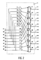
- the eight read outputs 41 to 48 (see FIG. 2) of the buffer memory 4 are connected to as many inputs of a selection matrix 5.
- Figure 2 shows an embodiment of such a selection matrix. It contains seven delay elements V1 to V7, which are connected to seven of their inputs 42 to 47. The delay elements V1 to V7 delay the bits at the inputs 42 to 47 of the selection matrix 5 by one clock period of the read clock. This results in a total of fifteen internal connection points Z1 to Z15 of the selection matrix.
- the selection matrix also contains eight 8: 1 selection circuits A1 to A8, the outputs of which are simultaneously the outputs 61 to 68 of the selection matrix 5.
- Each of the selection circuits A1 to A8 has eight inputs, each of which is connected to one of the connection points Z1 to Z15.
- the selection circuit A1 is connected to the connection points Z1 to Z8 (only the first and the last connection are shown in FIG.
- the second selection circuit is connected to the connection points Z2 to Z9 etc. up to the selection circuit A8 which is connected to the Connection points Z8 to Z15 is connected.
- the selection circuits A1 to A8 connect - controlled by addresses - one of their inputs to their output.
- the control lines for the selection circuits A1 to A8 and clock supply lines are not shown in FIG. 2.
- the table according to FIG. 3 serves to explain the mode of operation of the selection matrix according to FIG. 2.
- the table according to FIG. 3 contains the connection points Z1 to Z15 in its left margin column.
- the top line shows numbers of clock periods of the reading clock, which are also used as column numbers.
- Column 1 shows the data that are present at terminals Z1 to Z15 during a first read clock period; these are bits a1 to a8 of the first byte read.
- the double border indicates that the bits of the first bytes in the order from top to bottom, in this case in the order a1 to a8, are passed on to the output lines 61 to 68 of the selection matrix 5 by appropriate setting of the selection circuits A1 to A8.
- This repeated bit is forwarded on line 61 and can remain unchanged if its value is not important (eg stuffing bit); otherwise it must be overwritten by a circuit arrangement, not shown, with a very specific value.
- bits C1 to C8 of a new byte appear at the terminals Z8 to Z15, whereas bits b2 to b8 of the previous byte are present at the terminals Z1 to Z7.
- the double-bordered part in the third column shows that the first bit is the bit b8 of the second byte, which was not transmitted in the previous reading cycle, is now transferred to line 61.
- the underlining of bit a8 means that the information transmitted by it is already known to the recipient and can therefore be overwritten if such an overwriting is necessary.
- FIG. 3 shows that the track number s can assume a total of eight different integer values. If the number of tracks is selected so that it receives the value 0 in the switching state according to column 1 and progressively runs through all the integer values until the switching state according to column 7, the number of tracks s simultaneously indicates the number of modulo 8 stuffing bits transmitted. If the number of tracks skips the number 7, as in the transition from column 7 to column 8 of FIG. 3, the read counter and the delay elements V1 to V7 are stopped for one cycle and in the example according to FIG. 3 the seventh byte is read out again, so that none Information is lost.
- the control circuit 15 thus sets the switching state of the switching matrix 5 by counting the additional bits to be transmitted with a track number counter modulo 8 and by giving control addresses for the selection circuits A1 to A8 in accordance with the status s of this counter.
- the distance criterion of the write and read addresses has priority over all other criteria. If the distance deviates from its setpoint, stuffing bits are inserted until the setpoint distance is reached. Because of the structure of the frame, only one bit per frame line can be stuffed, so that - mostly when the arrangement is started up - a very long stuffing has to be done. In this case, the track number counter continuously and cyclically runs through all values from zero to seven. When the jump from seven to zero - compare the table in FIG. 3 - the read counter 13 and the delay elements V1 to V7 are stopped for one clock. The control circuit 15 also takes over the stopping of the read counter 13.
- Another criterion for increasing the number of tracks is the frequency difference between the write and read clock or the bit clock of the first signal and the bit clock of the second signal. With the aid of the phase comparator 16 and the control circuit 15, a decision is made as to whether or not to stuff because of this difference.
- the phase comparator 16 alone only compares the write and read clock and continuously outputs the result of this comparison to the control device 15. If the phase comparator 16 signals that stuffing is to take place - in other words, if there is a flank of the reading clock from the corresponding flank of the slower writing clock - then if a bit is really stuffed, the reading clock should be stopped for the duration of a bit (on the Timeline shifted) so that the distance is shortened accordingly and incorrect decisions are not made due to the absence of the shortening. Stopping the reading pulse for the duration of one bit (of the second signal) would, however, again require fast components which the circuit just avoided should be. Therefore there is no shifting of the reading pulse; Which equivalent measures are taken as an alternative can be found in the explanations below. Before doing so, however, one aspect of jitter in the recovered first signal on the receiver side will be discussed.
- bits may only be stuffed at a certain point in the frame lines.
- the recipient is informed by the stuffing information bits mentioned above whether the bit at the stuffing point is a stuffing bit or an information bit. For this reason, the decision whether to stop or not (darning decision) must be made on the order of a frame length in front of the darning point. If the time of this decision randomly fluctuates relative to the frame, this results in an additional jitter, the so-called waiting time jitter (see: Duttweiler, DL: Waiting Time Jitter. Bell Syst. Tech. J. 51, (1972), page 165 to 207). It is therefore desirable that the decision whether to insert a stuff bit or an information bit at the stuffing point is always made at the same time interval before this point.
- this additional jitter (waiting time jitter) is avoided, however, by systematically varying the point in time that is decisive for the stuffing decision. This variation is based on the following considerations:
- edges can be specified in it, each at a sufficient distance from the Darning points are located and are always at the same distance from them.
- These edges - hereinafter referred to as reference edges - are recognized by the control unit 15 (by counting the edges with the beginning of a line), which evaluates the output signal of the phase comparator 16 when the m th edge occurs relative to a reference edge, that is, at this point in time he sign of the phase position of the writing cycle to the (undisplaced) reading cycle and the knowledge of this sign makes the darning decision.
- the integer m searched for results from the requirement that the amount of the expression m * TL / TS - k - s / 8 as a function of the integers m and k should be as small as possible.
- TL means the period of the reading cycle
- TS the period of the writing cycle
- s the number of tracks mentioned above.
- the requirement itself can be derived from a consideration of the phase difference between the write clock and a read clock shifted by s bit at the time of a reference edge.
- the division of the track number s by 8 is related to the reduction of the bit clocks in a ratio of 1: 8. In the case of a generalization, this 8 must be replaced by n.
- the range of the permitted m and k values is to be selected such that the expression given can be made sufficiently small for all s from zero to seven, since it is a measure of the phase error which the present arrangement makes compared to an arrangement, in which the bit numbers are compared.
- the m (s) determined in this way is stored in a memory of the control circuit 15, which is also implemented only in CMOS technology.
- the track number s thus determines the edge of the reading pulse at which the phase comparator 16 is queried and the switching state of the selection matrix 5.
- an incoming binary signal arriving at a terminal 41 is fed to a series-parallel converter 42 on the receiver side of a transmission system.
- This first binary signal has a nominal bit rate of 155.52 Mbit / s and is one of four STM-1 signals which result after a STM-4 signal has been broken down by a demultiplexer, not shown.
- the arrangement according to FIG. 4 is supplied with the bit clock of the first binary signal provided with clock gaps via a terminal 410 and the stuffing information bits obtained from the first binary signal via a terminal 418.
- the stuffing information bits and the clocked bit clock are obtained from the transmitted STM-4 signal by an arrangement, not shown, associated with the demultiplexer.
- Terminal 418 is connected to a control device 415, which essentially consists of a cyclically running track number counter, with the aid of which the switching state of a selection matrix 45 is set.
- the track number counter is clocked with the byte clock which results from the bit clock of the first binary signal after division in a ratio of 1: 8 by a divider 411.
- the gaps in the bit clock at terminal 410 are distributed in such a way that after the clock is reduced at the output of divider 411, there is a byte clock with byte clock gaps.
- the Control device 415 For orientation in the current frame of the first binary signal, the Control device 415 the necessary information supplied via a terminal 419. The unit that supplies this information is also assigned to the demultiplexer.
- the selection matrix 45 is constructed according to the same principle as the selection matrix 5 in FIGS. 1 and 2.
- the first binary signal is transferred from the series-parallel converter 42 to the selection matrix 45 on lines 431 to 438. Controlled by a write counter 412, which is clocked by the gapped byte clock, the first binary signal is then written into a buffer memory 44 byte by byte without stuffing bytes.
- a read counter 413 controls the byte-by-byte readout from the buffer memory 44. The bytes read out are forwarded via lines 461 to 468 to a parallel-series converter 47, at the output 48 of which the second binary signal with a nominal bit rate of 139.264 Mbit / s is present.
- a phase comparator 49 is part of a phase-locked loop, not shown, with the aid of which the (gapless) bit clock of the second binary signal is obtained. This bit clock is present at terminal 417. It is divided down by a divider 414 in a 1: 8 ratio.
- the read counter 413 is supplied with the divided clock and the parallel-series converter 47 with the divided and undivided clock
Landscapes
- Engineering & Computer Science (AREA)
- Computer Networks & Wireless Communication (AREA)
- Signal Processing (AREA)
- Time-Division Multiplex Systems (AREA)
- Synchronisation In Digital Transmission Systems (AREA)
- Dc Digital Transmission (AREA)
- Data Exchanges In Wide-Area Networks (AREA)
- Communication Control (AREA)
- Stabilization Of Oscillater, Synchronisation, Frequency Synthesizers (AREA)
Claims (13)
- Montage de circuit d'adaptation des débits binaires de deux signaux, comportant:- un convertisseur série/parallèle (2) pour convertir respectivement n bits sériels d'un premier signal en un groupe de n bits parallèles;- une mémoire élastique (4) pour, respectivement, traduire et extraire un groupe de bits parallèles;- une matrice de sélection (5) délivrant un deuxième signal, qui est destinée, lors d'une opération de bourrage, à retarder certains bits de groupes successifs de bits parallèles et à introduire des bits de bourrage en lieu et place des bits déterminés, et- un dispositif de commande (15) pour commander l'opération d'extraction de la mémoire élastique (4) et de la matrice de sélection (5) en fonction d'une comparaison de phase d'un rythme d'écriture et d'un rythme de lecture à un moment se trouvant toujours à une distance dans le temps égale d'un emplacement de bourrage, et d'un contrôle de l'état de remplissage (8) de la mémoire élastique (4).
- Montage de circuit d'adaptation des rythmes binaires de deux signaux selon la revendication 1, caractérisé en ce que des diviseurs (11, 14), qui présentent un rapport de division de 1:n, sont respectivement destinés à produire le rythme d'écriture à partir du rythme binaire du premier signal et le rythme de lecture à partir du rythme binaire du deuxième signal.
- Montage de circuit d'adaptation des débits binaires de deux signaux selon la revendication 2, caractérisé en ce qu'un comparateur de phase (16) est destiné à comparer les phases du rythme d'écriture et du rythme de lecture, et en ce que le dispositif de commande (15) évalue le signal de sortie du comparateur de phase (16) à l'apparition d'un flanc prédéterminé et règle la matrice de sélection pour l'insertion d'au moins un bit de bourrage lorsque le contrôle de l'état de remplissage (8) constate un écart trop important de la valeur prescrite.
- Montage de circuit d'adaptation des débits binaires de deux signaux selon la revendication 3, caractérisé en ce que le dispositif de commande (15) est destiné à augmenter le nombre de traces (s) d'une unité modulo n par bit de bourrage et à répéter l'extraction d'un groupe de bits de la mémoire élastique (4) lorsque le nombre de traces s saute la valeur n - 1.
- Montage de circuit d'adaptation des débits binaires de deux signaux selon la revendication 4, caractérisé en ce que le flanc prédéterminé est le mème flanc par rapport à un flanc de référence du rythme de lecture, où m résulte de l'exigence que la valeur absolue de l'expression

- Montage de circuit d'adaptation des débits binaires de deux signaux selon l'une quelconque des revendications 1 à 5, caractérisé en ce que la mémoire élastique (4) est une mémoire tampon adressable, qui est destinée à recevoir des adresses d'écriture d'un compteur d'écriture (12) recevant le rythme d'écriture et des adresses de lecture d'un compteur de lecture (13) recevant le rythme de lecture.
- Montage de circuit d'adaptation des débits binaires de deux signaux selon la revendication 6, caractérisé en ce que le contrôle de l'état de remplissage (9) sert à comparer les adresses d'écriture et de lecture et, dans le cas d'un écart vis-à-vis d'une différence prescrite d'adresses, à délivrer un signal au dispositif de commande (15), et en ce que le dispositif de commande (15) sert à régler la différence d'adresse par une modification de l'état de commutation de la matrice de sélection (5) et par un arrêt du compteur de lecture (13).
- Montage de circuit d'adaptation des rythmes binaires de deux signaux selon l'une quelconque des revendications 1 à 7, caractérisé en ce que la matrice de sélection (5) est couplée à un convertisseur parallèle/série (7) pour convertir respectivement un groupe de n bits parallèles en respectivement n bits sériels d'un deuxième signal.
- Montage de circuit d'adaptation des débits binaires de deux signaux comportant:- un convertisseur série/parallèle (42) pour convertir respectivement n bits sériels d'un signal en un groupe de n bits parallèles;- une matrice de sélection (45), qui est destinée, lors d'une opération de débourrage, à retarder certains bits de groupes successifs de bits parallèles du premier signal et à transmettre des groupes de bits parallèles à l'exception des bits de bourrage;- une mémoire élastique (44) pour, respectivement, inscrire un groupe de bits parallèles délivré par la matrice de sélection (45) et extraire un groupe de bits parallèles pour un deuxième signal;- un dispositif de commande (415) pour recevoir des bits d'informations de bourrage et pour commander la matrice de sélection (45), et- une boucle à phase asservie pour commander la transcription des bits de la mémoire élastique (44).
- Montage de circuit d'adaptation des débits binaires de deux signaux selon la revendication 9, caractérisé en ce que des diviseurs (411, 414), qui présentent un rapport de division de 1:n, sont respectivement prévus pour produire le rythme d'écriture à partir du rythme binaire du premier signal et le rythme de lecture à partir du rythme binaire du deuxième signal.
- Montage de circuit d'adaptation des débits binaires de deux signaux selon la revendication 10, caractérisé en ce qu'un comparateur de phase (49) est prévu pour comparer en phase les adresses délivrées par un compteur d'écriture (412) et par un compteur de lecture (413) et pour obtenir le rythme binaire pour le deuxième signal.
- Montage de circuit d'adaptation des débits binaires de deux signaux selon la revendication 11, caractérisé en ce que la mémoire élastique (44) est une mémoire tampon adressable, qui est destinée à recevoir les adresses d'écriture du compteur d'écriture (412) et les adresses de lecture du compteur de lecture (413).
- Montage de circuit d'adaptation des débits binaires de deux signaux selon l'une quelconque des revendications 9 à 12, caractérisé en ce que la mémoire élastique (44) est couplée à un convertisseur parallèle/série (47) pour convertir respectivement un groupe de n bits parallèles en respectivement n bits sériels d'un deuxième signal.
Applications Claiming Priority (2)
| Application Number | Priority Date | Filing Date | Title |
|---|---|---|---|
| DE3920391A DE3920391A1 (de) | 1989-06-22 | 1989-06-22 | Schaltungsanordnung zur anpassung der bitraten zweier signale |
| DE3920391 | 1989-06-22 |
Publications (3)
| Publication Number | Publication Date |
|---|---|
| EP0404268A2 EP0404268A2 (fr) | 1990-12-27 |
| EP0404268A3 EP0404268A3 (fr) | 1991-10-09 |
| EP0404268B1 true EP0404268B1 (fr) | 1996-02-07 |
Family
ID=6383289
Family Applications (1)
| Application Number | Title | Priority Date | Filing Date |
|---|---|---|---|
| EP90201626A Expired - Lifetime EP0404268B1 (fr) | 1989-06-22 | 1990-06-21 | Dispositif d'adaptation des débits de deux signaux |
Country Status (4)
| Country | Link |
|---|---|
| EP (1) | EP0404268B1 (fr) |
| JP (1) | JPH03129934A (fr) |
| DE (2) | DE3920391A1 (fr) |
| ES (1) | ES2085883T3 (fr) |
Families Citing this family (8)
| Publication number | Priority date | Publication date | Assignee | Title |
|---|---|---|---|---|
| DE4027967A1 (de) * | 1990-09-04 | 1992-03-05 | Philips Patentverwaltung | Stopfentscheidungsschaltung fuer eine anordnung zur bitratenanpassung |
| JPH04286233A (ja) * | 1991-03-14 | 1992-10-12 | Nec Corp | スタッフ同期回路 |
| DE4205959A1 (de) * | 1992-02-27 | 1993-09-02 | Philips Patentverwaltung | Schaltungsanordnung zum ausgleich von frequenz- und/oder phasenschwankungen zwischen einem ankommenden und einem abgehenden signal |
| US5285206A (en) * | 1992-08-25 | 1994-02-08 | Alcatel Network Systems, Inc. | Phase detector for elastic store |
| DE4425087A1 (de) * | 1994-07-15 | 1996-01-18 | Philips Patentverwaltung | Übertragungssystem |
| EP0702465A1 (fr) * | 1994-09-13 | 1996-03-20 | T.R.T. Telecommunications Radioelectriques Et Telephoniques | Système de transmission et équipement de multiplexage-démultiplexage impliquant un flux d'éléments binaires pouvant être justifié |
| DE19707365C2 (de) * | 1997-02-25 | 1999-01-07 | Lucent Tech Network Sys Gmbh | Digitaler Oszillator |
| DE19719547C1 (de) * | 1997-05-09 | 1998-11-12 | Lucent Tech Network Sys Gmbh | Digitaler Oszillator |
Family Cites Families (3)
| Publication number | Priority date | Publication date | Assignee | Title |
|---|---|---|---|---|
| FR2269246B1 (fr) * | 1974-04-25 | 1976-12-17 | Cit Alcatel | |
| US4397017A (en) * | 1981-03-02 | 1983-08-02 | Nippon Electric Co., Ltd. | Stuff synchronization device with reduced sampling jitter |
| DE3843372C2 (de) * | 1988-12-23 | 1997-03-27 | Bosch Gmbh Robert | Verfahren und Schaltungsanordnung zur Taktanpassung in der digitalen Nachrichtentechnik |
-
1989
- 1989-06-22 DE DE3920391A patent/DE3920391A1/de not_active Withdrawn
-
1990
- 1990-06-21 DE DE59010110T patent/DE59010110D1/de not_active Expired - Fee Related
- 1990-06-21 ES ES90201626T patent/ES2085883T3/es not_active Expired - Lifetime
- 1990-06-21 EP EP90201626A patent/EP0404268B1/fr not_active Expired - Lifetime
- 1990-06-22 JP JP2163005A patent/JPH03129934A/ja active Pending
Also Published As
| Publication number | Publication date |
|---|---|
| DE3920391A1 (de) | 1991-01-10 |
| EP0404268A3 (fr) | 1991-10-09 |
| EP0404268A2 (fr) | 1990-12-27 |
| DE59010110D1 (de) | 1996-03-21 |
| JPH03129934A (ja) | 1991-06-03 |
| ES2085883T3 (es) | 1996-06-16 |
Similar Documents
| Publication | Publication Date | Title |
|---|---|---|
| EP0507385B1 (fr) | Système de transmission pour la hiérarchie numérique synchrone | |
| DE69327479T2 (de) | Verfahren zum zerlegen und zusammensetzen von rahmenstrukturen mit zeigern | |
| EP0503732B1 (fr) | Méthode et système de transmission pour la hiérarchie numérique synchrone | |
| DE69836157T2 (de) | Verfahren und Vorrichtung zum Demultiplexen digitaler Signalströme | |
| EP0429888B1 (fr) | Méthode de transmission par un réseau multiplex hierarchisé synchrone et numérique d'un signal à large bande distribué entre des unités de transmission subordonnées | |
| EP0475497B1 (fr) | Circuit de décision de justification pour un dispositif d'adaption de débit binaire | |
| DE69104721T2 (de) | Verfahren und anordnung für datensynchronisierung. | |
| DE3151207C2 (de) | Speicheranordnung für eine PCM-Fernmeldevermittlungsanlage | |
| EP0408130B1 (fr) | Dispositif d'adaptation du débit binaire de deux signaux | |
| EP0475498B1 (fr) | Circuit d'adaption du débit binaire de deux signaux numériques | |
| DE3934248A1 (de) | Multiplexer und demultiplexer, insbesondere fuer nachrichtenuebertragungs-netze mit einer synchronen hierarchie der digitalsignale | |
| EP0708541B1 (fr) | Système de transmission avec une boucle de commande | |
| EP0435383B1 (fr) | Circuit d'adaptation de débit binaire | |
| EP0639903A2 (fr) | Système de transmission | |
| DE69220267T2 (de) | Pulsstopfanlage | |
| EP0404268B1 (fr) | Dispositif d'adaptation des débits de deux signaux | |
| DE69225186T2 (de) | Endstationssynchronisierungsanordnung in einem digitalen asynchronen Übertragungsnetz | |
| EP0598455B1 (fr) | Système de transmission pour la hiérarchie numérique synchrone | |
| EP1051057A2 (fr) | Transport de conteneurs concaténées dans une réseau de transmission synchrone | |
| DE2412962B2 (de) | Verfahren zur zeitmultiplex-uebertragung von daten | |
| DE2752996A1 (de) | Digitale multiplexiervorrichtung fuer plesiochrone bitfolgen | |
| DE3843372C2 (de) | Verfahren und Schaltungsanordnung zur Taktanpassung in der digitalen Nachrichtentechnik | |
| EP1223698B1 (fr) | Procédé et module de compensation de phase des signaux d'horloge | |
| DE2908366C2 (de) | Verfahren und Schaltungsanordnung zur Reduzierung von Phasenschwankungen bei der Taktrückgewinnung in einem digitalen, hierarchisch gegliederten, plesiochronen Nachrichtenübertragungssystem | |
| EP1094610A1 (fr) | Boucle de verrouillage de phase numérique |
Legal Events
| Date | Code | Title | Description |
|---|---|---|---|
| PUAI | Public reference made under article 153(3) epc to a published international application that has entered the european phase |
Free format text: ORIGINAL CODE: 0009012 |
|
| AK | Designated contracting states |
Kind code of ref document: A2 Designated state(s): DE ES FR GB |
|
| PUAL | Search report despatched |
Free format text: ORIGINAL CODE: 0009013 |
|
| AK | Designated contracting states |
Kind code of ref document: A3 Designated state(s): DE ES FR GB |
|
| 17P | Request for examination filed |
Effective date: 19920409 |
|
| 17Q | First examination report despatched |
Effective date: 19940216 |
|
| GRAA | (expected) grant |
Free format text: ORIGINAL CODE: 0009210 |
|
| AK | Designated contracting states |
Kind code of ref document: B1 Designated state(s): DE ES FR GB |
|
| REF | Corresponds to: |
Ref document number: 59010110 Country of ref document: DE Date of ref document: 19960321 |
|
| GBT | Gb: translation of ep patent filed (gb section 77(6)(a)/1977) |
Effective date: 19960424 |
|
| ET | Fr: translation filed | ||
| REG | Reference to a national code |
Ref country code: ES Ref legal event code: FG2A Ref document number: 2085883 Country of ref document: ES Kind code of ref document: T3 |
|
| PLBE | No opposition filed within time limit |
Free format text: ORIGINAL CODE: 0009261 |
|
| STAA | Information on the status of an ep patent application or granted ep patent |
Free format text: STATUS: NO OPPOSITION FILED WITHIN TIME LIMIT |
|
| 26N | No opposition filed | ||
| REG | Reference to a national code |
Ref country code: GB Ref legal event code: 732E |
|
| REG | Reference to a national code |
Ref country code: FR Ref legal event code: TP |
|
| REG | Reference to a national code |
Ref country code: ES Ref legal event code: PC2A |
|
| REG | Reference to a national code |
Ref country code: GB Ref legal event code: IF02 |
|
| PGFP | Annual fee paid to national office [announced via postgrant information from national office to epo] |
Ref country code: FR Payment date: 20020524 Year of fee payment: 13 |
|
| PGFP | Annual fee paid to national office [announced via postgrant information from national office to epo] |
Ref country code: GB Payment date: 20020527 Year of fee payment: 13 |
|
| PGFP | Annual fee paid to national office [announced via postgrant information from national office to epo] |
Ref country code: ES Payment date: 20020604 Year of fee payment: 13 |
|
| PGFP | Annual fee paid to national office [announced via postgrant information from national office to epo] |
Ref country code: DE Payment date: 20020628 Year of fee payment: 13 |
|
| PG25 | Lapsed in a contracting state [announced via postgrant information from national office to epo] |
Ref country code: GB Free format text: LAPSE BECAUSE OF NON-PAYMENT OF DUE FEES Effective date: 20030621 |
|
| PG25 | Lapsed in a contracting state [announced via postgrant information from national office to epo] |
Ref country code: ES Free format text: LAPSE BECAUSE OF NON-PAYMENT OF DUE FEES Effective date: 20030623 |
|
| PG25 | Lapsed in a contracting state [announced via postgrant information from national office to epo] |
Ref country code: DE Free format text: LAPSE BECAUSE OF NON-PAYMENT OF DUE FEES Effective date: 20040101 |
|
| GBPC | Gb: european patent ceased through non-payment of renewal fee |
Effective date: 20030621 |
|
| PG25 | Lapsed in a contracting state [announced via postgrant information from national office to epo] |
Ref country code: FR Free format text: LAPSE BECAUSE OF NON-PAYMENT OF DUE FEES Effective date: 20040227 |
|
| REG | Reference to a national code |
Ref country code: FR Ref legal event code: ST |
|
| REG | Reference to a national code |
Ref country code: ES Ref legal event code: FD2A Effective date: 20030623 |