EP0406060A1 - Magnetwiderstandseffektwandler - Google Patents
Magnetwiderstandseffektwandler Download PDFInfo
- Publication number
- EP0406060A1 EP0406060A1 EP90401712A EP90401712A EP0406060A1 EP 0406060 A1 EP0406060 A1 EP 0406060A1 EP 90401712 A EP90401712 A EP 90401712A EP 90401712 A EP90401712 A EP 90401712A EP 0406060 A1 EP0406060 A1 EP 0406060A1
- Authority
- EP
- European Patent Office
- Prior art keywords
- magnetoresistive effect
- layers
- effect sensor
- sensor according
- magnetic material
- Prior art date
- Legal status (The legal status is an assumption and is not a legal conclusion. Google has not performed a legal analysis and makes no representation as to the accuracy of the status listed.)
- Granted
Links
- 230000000694 effects Effects 0.000 title claims description 29
- 230000005291 magnetic effect Effects 0.000 claims abstract description 46
- 239000000696 magnetic material Substances 0.000 claims abstract description 36
- 230000007704 transition Effects 0.000 claims abstract description 14
- 230000008878 coupling Effects 0.000 claims abstract description 10
- 238000010168 coupling process Methods 0.000 claims abstract description 10
- 238000005859 coupling reaction Methods 0.000 claims abstract description 10
- 230000005290 antiferromagnetic effect Effects 0.000 claims abstract description 7
- XEEYBQQBJWHFJM-UHFFFAOYSA-N Iron Chemical compound [Fe] XEEYBQQBJWHFJM-UHFFFAOYSA-N 0.000 claims description 14
- 229910052751 metal Inorganic materials 0.000 claims description 13
- 239000002184 metal Substances 0.000 claims description 13
- 230000005415 magnetization Effects 0.000 claims description 11
- PXHVJJICTQNCMI-UHFFFAOYSA-N Nickel Chemical compound [Ni] PXHVJJICTQNCMI-UHFFFAOYSA-N 0.000 claims description 10
- 229910052742 iron Inorganic materials 0.000 claims description 6
- 239000000463 material Substances 0.000 claims description 6
- 239000000758 substrate Substances 0.000 claims description 6
- 239000011651 chromium Substances 0.000 claims description 5
- 229910052759 nickel Inorganic materials 0.000 claims description 5
- 229910017052 cobalt Inorganic materials 0.000 claims description 4
- 239000010941 cobalt Substances 0.000 claims description 4
- GUTLYIVDDKVIGB-UHFFFAOYSA-N cobalt atom Chemical compound [Co] GUTLYIVDDKVIGB-UHFFFAOYSA-N 0.000 claims description 4
- 238000000034 method Methods 0.000 claims description 4
- VYZAMTAEIAYCRO-UHFFFAOYSA-N Chromium Chemical compound [Cr] VYZAMTAEIAYCRO-UHFFFAOYSA-N 0.000 claims description 3
- RTAQQCXQSZGOHL-UHFFFAOYSA-N Titanium Chemical compound [Ti] RTAQQCXQSZGOHL-UHFFFAOYSA-N 0.000 claims description 3
- 229910052804 chromium Inorganic materials 0.000 claims description 3
- WPBNNNQJVZRUHP-UHFFFAOYSA-L manganese(2+);methyl n-[[2-(methoxycarbonylcarbamothioylamino)phenyl]carbamothioyl]carbamate;n-[2-(sulfidocarbothioylamino)ethyl]carbamodithioate Chemical compound [Mn+2].[S-]C(=S)NCCNC([S-])=S.COC(=O)NC(=S)NC1=CC=CC=C1NC(=S)NC(=O)OC WPBNNNQJVZRUHP-UHFFFAOYSA-L 0.000 claims description 3
- 238000001451 molecular beam epitaxy Methods 0.000 claims description 3
- 229910052719 titanium Inorganic materials 0.000 claims description 3
- 239000010936 titanium Substances 0.000 claims description 3
- 229910052720 vanadium Inorganic materials 0.000 claims description 3
- LEONUFNNVUYDNQ-UHFFFAOYSA-N vanadium atom Chemical compound [V] LEONUFNNVUYDNQ-UHFFFAOYSA-N 0.000 claims description 3
- 238000005538 encapsulation Methods 0.000 claims description 2
- 239000011810 insulating material Substances 0.000 claims description 2
- 239000004065 semiconductor Substances 0.000 claims description 2
- 238000000151 deposition Methods 0.000 claims 1
- 230000008021 deposition Effects 0.000 claims 1
- 229910045601 alloy Inorganic materials 0.000 description 7
- 239000000956 alloy Substances 0.000 description 7
- 230000010287 polarization Effects 0.000 description 4
- 239000013078 crystal Substances 0.000 description 3
- 230000005294 ferromagnetic effect Effects 0.000 description 3
- JBRZTFJDHDCESZ-UHFFFAOYSA-N AsGa Chemical compound [As]#[Ga] JBRZTFJDHDCESZ-UHFFFAOYSA-N 0.000 description 2
- 238000000407 epitaxy Methods 0.000 description 2
- 239000003302 ferromagnetic material Substances 0.000 description 2
- 239000012535 impurity Substances 0.000 description 2
- 229910001218 Gallium arsenide Inorganic materials 0.000 description 1
- 229910017709 Ni Co Inorganic materials 0.000 description 1
- 239000002772 conduction electron Substances 0.000 description 1
- 230000001419 dependent effect Effects 0.000 description 1
- 238000009792 diffusion process Methods 0.000 description 1
- 230000005381 magnetic domain Effects 0.000 description 1
- 150000002739 metals Chemical class 0.000 description 1
- 229910052723 transition metal Inorganic materials 0.000 description 1
- 150000003624 transition metals Chemical class 0.000 description 1
Images

Classifications
-
- G—PHYSICS
- G01—MEASURING; TESTING
- G01R—MEASURING ELECTRIC VARIABLES; MEASURING MAGNETIC VARIABLES
- G01R33/00—Arrangements or instruments for measuring magnetic variables
- G01R33/02—Measuring direction or magnitude of magnetic fields or magnetic flux
- G01R33/06—Measuring direction or magnitude of magnetic fields or magnetic flux using galvano-magnetic devices
- G01R33/09—Magnetoresistive devices
- G01R33/093—Magnetoresistive devices using multilayer structures, e.g. giant magnetoresistance sensors
-
- B—PERFORMING OPERATIONS; TRANSPORTING
- B82—NANOTECHNOLOGY
- B82Y—SPECIFIC USES OR APPLICATIONS OF NANOSTRUCTURES; MEASUREMENT OR ANALYSIS OF NANOSTRUCTURES; MANUFACTURE OR TREATMENT OF NANOSTRUCTURES
- B82Y25/00—Nanomagnetism, e.g. magnetoimpedance, anisotropic magnetoresistance, giant magnetoresistance or tunneling magnetoresistance
-
- G—PHYSICS
- G11—INFORMATION STORAGE
- G11B—INFORMATION STORAGE BASED ON RELATIVE MOVEMENT BETWEEN RECORD CARRIER AND TRANSDUCER
- G11B5/00—Recording by magnetisation or demagnetisation of a record carrier; Reproducing by magnetic means; Record carriers therefor
- G11B5/127—Structure or manufacture of heads, e.g. inductive
- G11B5/33—Structure or manufacture of flux-sensitive heads, i.e. for reproduction only; Combination of such heads with means for recording or erasing only
- G11B5/39—Structure or manufacture of flux-sensitive heads, i.e. for reproduction only; Combination of such heads with means for recording or erasing only using magneto-resistive devices or effects
- G11B5/3903—Structure or manufacture of flux-sensitive heads, i.e. for reproduction only; Combination of such heads with means for recording or erasing only using magneto-resistive devices or effects using magnetic thin film layers or their effects, the films being part of integrated structures
-
- H—ELECTRICITY
- H10—SEMICONDUCTOR DEVICES; ELECTRIC SOLID-STATE DEVICES NOT OTHERWISE PROVIDED FOR
- H10N—ELECTRIC SOLID-STATE DEVICES NOT OTHERWISE PROVIDED FOR
- H10N50/00—Galvanomagnetic devices
- H10N50/80—Constructional details
- H10N50/85—Materials of the active region
-
- Y—GENERAL TAGGING OF NEW TECHNOLOGICAL DEVELOPMENTS; GENERAL TAGGING OF CROSS-SECTIONAL TECHNOLOGIES SPANNING OVER SEVERAL SECTIONS OF THE IPC; TECHNICAL SUBJECTS COVERED BY FORMER USPC CROSS-REFERENCE ART COLLECTIONS [XRACs] AND DIGESTS
- Y10—TECHNICAL SUBJECTS COVERED BY FORMER USPC
- Y10S—TECHNICAL SUBJECTS COVERED BY FORMER USPC CROSS-REFERENCE ART COLLECTIONS [XRACs] AND DIGESTS
- Y10S428/00—Stock material or miscellaneous articles
- Y10S428/922—Static electricity metal bleed-off metallic stock
- Y10S428/9265—Special properties
- Y10S428/928—Magnetic property
-
- Y—GENERAL TAGGING OF NEW TECHNOLOGICAL DEVELOPMENTS; GENERAL TAGGING OF CROSS-SECTIONAL TECHNOLOGIES SPANNING OVER SEVERAL SECTIONS OF THE IPC; TECHNICAL SUBJECTS COVERED BY FORMER USPC CROSS-REFERENCE ART COLLECTIONS [XRACs] AND DIGESTS
- Y10—TECHNICAL SUBJECTS COVERED BY FORMER USPC
- Y10T—TECHNICAL SUBJECTS COVERED BY FORMER US CLASSIFICATION
- Y10T428/00—Stock material or miscellaneous articles
- Y10T428/12—All metal or with adjacent metals
- Y10T428/12493—Composite; i.e., plural, adjacent, spatially distinct metal components [e.g., layers, joint, etc.]
- Y10T428/12632—Four or more distinct components with alternate recurrence of each type component
Definitions
- the present invention relates to magnetoresistive effect sensors, namely sensors using the variation of resistivity of the material forming the sensor as a function of the variation of a magnetic field.
- sensors using the magnetoresistive effect are implemented in various magnetic recording reading systems. These sensors are made of a ferromagnetic alloy with high magneto-resistance which is placed in the magnetic circuit of a read head. In this case, the variations of the electrical resistance of the sensor during the passage of the strip are detected.
- the high magnetoresistance alloys currently used are generally nickel-based ferromagnetic alloys, such as Ni80FE20 alloys or Ni Co alloys for which the magnetoresistance at ambient temperature corresponds to a resistance variation of a few percent.
- the object of the present invention is to overcome these drawbacks by proposing a new structure for the sensitive element of magneto-resistive effect sensors.
- the subject of the present invention is a sensor with a magnetoresistive effect, characterized in that the sensitive element of the sensor consists of a monocrystalline magnetic metal multilayer formed of a stack of layers made of a magnetic material separated by layers of a material non-magnetic, the multilayer being made such that the magnetic material layers have an anti-ferromagnetic type coupling and that the transition between the state of antiparallel arrangement and the parallel arrangement state is realized over a very small magnetic field interval.
- the magnetic material used in the magnetic metal multilayer is selected from iron, cobalt or nickel and the non-magnetic material is selected from manganese, chromium, vanadium or titanium.
- the layers of magnetic material have a thickness of 9 and 90 ⁇ and the layers of non-magnetic material have a thickness of less than 30 ⁇ .
- the layers of magnetic material are alternately thin and thick with a ratio between the thicknesses of between 1 and 3.
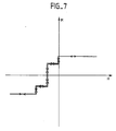
- the transition between the anti-parallel setting state and the parallel arrangement state will be of the "spin-flop" type (namely: by sudden reversal of the magnetization of the thin layers to a given field called spin-flop field).
- the layers of magnetic material are of the same thickness, the multilayer then having a uni-axial anisotropy in the plane of the layers.
- the magnetic metal multilayer is covered at least one additional magnetization-locked layer.
- the spin-flop magnetic field is shifted to very weak fields. This solution makes it possible to reduce or even possibly eliminate the necessary magnetic field of polarization when the system does not operate near a zero field.
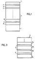
- a magnetoresistive effect sensor essentially comprises a substrate 1, a monocrystalline magnetic metal multilayer 2 formed by a stack of layers 20 of magnetic material separated by layers 21 of non-magnetic material, and covered with an encapsulation layer 3.
- the substrate 1 is made of either an insulating material or a material undoped semiconductor such as gallium arsenide (AsGa).
- the substrate 1 On this substrate 1 is deposited a monocrystalline magnetic metal multilayer.
- the substrate 1 must have a mesh structure adapted so that the growth of the multilayer is performed so as to obtain a single crystal.
- growth techniques such as epitaxial growth, preferably molecular beam epitaxy, also called MBE epitaxy, are used.
- MBE epitaxy molecular beam epitaxy
- the magnetic material of the layers 20 is chosen from iron, cobalt, nickel or an alloy of these metals, likewise the non-magnetic material of the layers 21 is chosen from manganese, chromium and vanadium. or titanium.
- the layers 20 of magnetic material have a thickness of between 9 and 90 ⁇ while the layers 21 of non-magnetic material have a thickness of less than 30 ⁇ so as to obtain a particular multilayer structure.
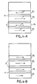
- FIG. 2A is of the anti-ferromagnetic type, that is to say that it has an arrangement anti-parallel symbolized by the arrows F and F 'in Figure 2A, for the magnetizations of the layers.
- the structure of the multilayer is such that it goes from the antiparallel arrangement of FIG. 2A to a parallel arrangement as shown in FIG. 2B for a very small magnetic field interval, some Gauss, or from FIG. 'a null field, either from a finite field. In this In the latter case, it is then necessary to use a bias magnetic field to fix the operating point of the sensor in the vicinity of this field.
- this multilayer has a particular structure and is made using ferromagnetic materials and non-magnetic materials that are specifically the magnetic material layers have an anti-ferromagnetic type coupling and the transition between the anti-parallel arrangement state and the parallel arrangement state occurs over a very small magnetic field gap.
- the basic element of a magnetoresistive sensor is furthermore subject to the fact that the coupling between the magnetic layers is of the anti-ferromagnetic type and that the transition between the antiparallel arrangement state and the parallel arrangement state occurs. performs on a very small field interval.
- non-magnetic layers made of any transition metal because of the high propensity that the electrons of the band layer d to magnetically polarize, will establish a coupling between magnetic layers for thicknesses of the same order of magnitude.
- this coupling may be a ferromagnetic coupling or an anti-ferromagnetic coupling, which explains the choice of non-magnetic materials.
- FIG. 3 shows an alternative embodiment of the monocrystalline magnetic metal multilayer 2 of a magnetoresistive effect sensor.
- the magnetic layers 20'1, 20'2, 20'3 and 20'4 consist of layers of varying thicknesses.
- the 20'1 and 20'3 layers are thick layers while the 20'1 and 20'4 layers are thin layers.
- the layers must be made so that their thickness is in a ratio of 1 to 3.
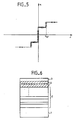
- obtaining a hysteresis cycle such as that shown in FIG. 5 can also be achieved with magnetic metal multilayers having magnetic layers of equal thickness, if the system has a uni-axial anisotropy in the plane of the layers as for example when the system is made with epitaxy of type (110) bcc or fcc.
- FIG. 6 there is shown a third embodiment of a magnetoresistive effect sensor according to the present invention.
- the magnetic metal multilayer 2 there is deposited at least one additional layer 4 (two in the embodiment) magnetization blocked in a given direction.
- This additional layer with locked magnetization is constituted, for example, by a thick layer of iron.
Landscapes
- Engineering & Computer Science (AREA)
- Physics & Mathematics (AREA)
- Chemical & Material Sciences (AREA)
- Nanotechnology (AREA)
- Condensed Matter Physics & Semiconductors (AREA)
- General Physics & Mathematics (AREA)
- Manufacturing & Machinery (AREA)
- Crystallography & Structural Chemistry (AREA)
- Hall/Mr Elements (AREA)
- Measuring Magnetic Variables (AREA)
- Magnetic Heads (AREA)
Applications Claiming Priority (2)
| Application Number | Priority Date | Filing Date | Title |
|---|---|---|---|
| FR8908545A FR2648942B1 (fr) | 1989-06-27 | 1989-06-27 | Capteur a effet magnetoresistif |
| FR8908545 | 1989-06-27 |
Publications (2)
| Publication Number | Publication Date |
|---|---|
| EP0406060A1 true EP0406060A1 (de) | 1991-01-02 |
| EP0406060B1 EP0406060B1 (de) | 1995-05-10 |
Family
ID=9383160
Family Applications (1)
| Application Number | Title | Priority Date | Filing Date |
|---|---|---|---|
| EP90401712A Expired - Lifetime EP0406060B1 (de) | 1989-06-27 | 1990-06-19 | Magnetwiderstandseffektwandler |
Country Status (5)
| Country | Link |
|---|---|
| US (1) | US5134533A (de) |
| EP (1) | EP0406060B1 (de) |
| JP (1) | JP3058338B2 (de) |
| DE (1) | DE69019242T2 (de) |
| FR (1) | FR2648942B1 (de) |
Cited By (20)
| Publication number | Priority date | Publication date | Assignee | Title |
|---|---|---|---|---|
| EP0498344A1 (de) * | 1991-02-04 | 1992-08-12 | Matsushita Electric Industrial Co., Ltd. | Magnetoresistives Element |
| EP0503499A1 (de) * | 1991-03-08 | 1992-09-16 | Matsushita Electric Industrial Co., Ltd. | Magnetresistive Materialien |
| EP0506433A1 (de) * | 1991-03-29 | 1992-09-30 | Kabushiki Kaisha Toshiba | Magnetowiderstandseffekt-Element |
| EP0483373A4 (en) * | 1990-05-21 | 1992-10-21 | Ube Industries Limited | Magnetoresistance effect element |
| FR2677811A1 (fr) * | 1991-06-11 | 1992-12-18 | Philips Electronique Lab | Dispositif incluant un super-reseau de couches ayant des proprietes de magnetoresistance geante realisees sur un substrat semiconducteur. |
| EP0539213A1 (de) * | 1991-10-23 | 1993-04-28 | Kabushiki Kaisha Toshiba | Magnetowiderstandseffekt-Element und Magnetowiderstandseffekt-Fühler |
| FR2693021A1 (fr) * | 1992-06-26 | 1993-12-31 | Thomson Csf | Détecteur de champ magnétique. |
| EP0578196A1 (de) * | 1992-07-07 | 1994-01-12 | Nec Corporation | Magnetoresistive Elemente und Verfahren zu ihrer Herstellung |
| EP0581295A1 (de) * | 1992-07-31 | 1994-02-02 | Sony Corporation | Magnetoresistive Schicht und Verfahren zur ihrer Herstellung |
| EP0598342A1 (de) * | 1992-11-16 | 1994-05-25 | Read-Rite Corporation | Magnetoresistiver Sensorkopf mit zwei Elementen |
| WO1994017426A1 (de) * | 1993-01-22 | 1994-08-04 | Siemens Aktiengesellschaft | Vorrichtung zum erfassen einer winkelposition eines objektes |
| EP0616484A1 (de) * | 1993-03-19 | 1994-09-21 | Thomson-Csf | Magnetoresistiver Wandler und Verfahren zu seiner Herstellung |
| EP0675554A1 (de) * | 1994-03-24 | 1995-10-04 | Nec Corporation | Element mit magnetoresistivem Effekt |
| EP0684484A3 (de) * | 1994-05-25 | 1996-01-10 | Eastman Kodak Co | |
| EP0660127A3 (de) * | 1993-12-23 | 1996-01-17 | Ibm | Mehrschicht magnetoresistiver Fühler. |
| EP0526044B1 (de) * | 1991-07-30 | 1996-06-12 | Kabushiki Kaisha Toshiba | Magnetoresistant-Effekt Element |
| EP0701235A3 (de) * | 1990-04-10 | 1996-11-13 | Knogo Corp | Verfahren und Einrichtung zur Herstellung und Nutzung von magnetischen Warensicherungsetiketten |
| EP0550306B1 (de) * | 1991-12-23 | 1997-05-14 | Thomson-Csf | Magnetoresistiver Fühler für schwache Magnetfelder |
| EP0721563A4 (de) * | 1993-10-01 | 1998-01-28 | Us Navy | Magnetoresistiver linearer weggeber, winkelverschiebungssensor und variabler widerstand |
| EP0560350B1 (de) * | 1992-03-13 | 2002-06-19 | Matsushita Electric Industrial Co., Ltd. | Magnetowiderstandeffekt-Element |
Families Citing this family (64)
| Publication number | Priority date | Publication date | Assignee | Title |
|---|---|---|---|---|
| US5390061A (en) | 1990-06-08 | 1995-02-14 | Hitachi, Ltd. | Multilayer magnetoresistance effect-type magnetic head |
| JP3483895B2 (ja) * | 1990-11-01 | 2004-01-06 | 株式会社東芝 | 磁気抵抗効果膜 |
| US5341261A (en) * | 1991-08-26 | 1994-08-23 | International Business Machines Corporation | Magnetoresistive sensor having multilayer thin film structure |
| US5633092A (en) * | 1991-12-10 | 1997-05-27 | British Technology Group Ltd. | Magnetostrictive material |
| US5287238A (en) * | 1992-11-06 | 1994-02-15 | International Business Machines Corporation | Dual spin valve magnetoresistive sensor |
| US5569544A (en) * | 1992-11-16 | 1996-10-29 | Nonvolatile Electronics, Incorporated | Magnetoresistive structure comprising ferromagnetic thin films and intermediate layers of less than 30 angstroms formed of alloys having immiscible components |
| US5617071A (en) * | 1992-11-16 | 1997-04-01 | Nonvolatile Electronics, Incorporated | Magnetoresistive structure comprising ferromagnetic thin films and intermediate alloy layer having magnetic concentrator and shielding permeable masses |
| EP0678213B1 (de) * | 1992-11-16 | 2003-02-19 | NVE Corporation | Magnetoresistive struktur mit einer legierungsschicht |
| FR2698965B1 (fr) * | 1992-12-03 | 1995-01-06 | Commissariat Energie Atomique | Structure et capteur magnétiques multicouches à forte magnétorésistance et procédé de fabrication de la structure. |
| US5432373A (en) * | 1992-12-15 | 1995-07-11 | Bell Communications Research, Inc. | Magnetic spin transistor |
| US5343422A (en) * | 1993-02-23 | 1994-08-30 | International Business Machines Corporation | Nonvolatile magnetoresistive storage device using spin valve effect |
| US5493465A (en) * | 1993-03-15 | 1996-02-20 | Kabushiki Kaisha Toshiba | Magnetoresistance effect element and magnetic recording apparatus |
| US5576915A (en) * | 1993-03-15 | 1996-11-19 | Kabushiki Kaisha Toshiba | Magnetoresistive head with antiferromagnetic sublayers interposed between first and second spin-valve units to exchange bias inner magnetic films thereof |
| US5736921A (en) * | 1994-03-23 | 1998-04-07 | Sanyo Electric Co., Ltd. | Magnetoresistive element |
| US5585198A (en) * | 1993-10-20 | 1996-12-17 | Sanyo Electric Co., Ltd. | Magnetorsistance effect element |
| JP2551321B2 (ja) * | 1993-04-21 | 1996-11-06 | 日本電気株式会社 | 集積化磁気抵抗効果センサ |
| US5949707A (en) * | 1996-09-06 | 1999-09-07 | Nonvolatile Electronics, Incorporated | Giant magnetoresistive effect memory cell |
| JPH0766033A (ja) * | 1993-08-30 | 1995-03-10 | Mitsubishi Electric Corp | 磁気抵抗素子ならびにその磁気抵抗素子を用いた磁性薄膜メモリおよび磁気抵抗センサ |
| US5585199A (en) * | 1993-09-09 | 1996-12-17 | Kabushiki Kaisha Toshiba | Magnetoresistance effect head |
| TW279977B (de) * | 1993-09-24 | 1996-07-01 | Philips Electronics Nv | |
| FR2710753B1 (fr) * | 1993-09-27 | 1995-10-27 | Commissariat Energie Atomique | Capteur de courant comprenant un ruban magnétorésistif et son procédé de réalisation. |
| WO1995010123A1 (en) | 1993-10-06 | 1995-04-13 | Philips Electronics N.V. | Magneto-resistance device, and magnetic head employing such a device |
| US5465185A (en) * | 1993-10-15 | 1995-11-07 | International Business Machines Corporation | Magnetoresistive spin valve sensor with improved pinned ferromagnetic layer and magnetic recording system using the sensor |
| US5408377A (en) * | 1993-10-15 | 1995-04-18 | International Business Machines Corporation | Magnetoresistive sensor with improved ferromagnetic sensing layer and magnetic recording system using the sensor |
| FR2712420B1 (fr) * | 1993-11-08 | 1995-12-15 | Commissariat Energie Atomique | Tête magnétique de lecture à élément magnétorésistant multicouche et à concentrateur et son procédé de réalisation. |
| US5313375A (en) * | 1993-11-10 | 1994-05-17 | Guth Lighting Inc. | Flow-thru troffer |
| EP0676746B1 (de) * | 1994-03-09 | 1999-08-04 | Eastman Kodak Company | Magnetoresistiver Wiedergabekopf mit doppeltem Spin-Ventilelement |
| JPH08511378A (ja) * | 1994-03-25 | 1996-11-26 | フィリップス エレクトロニクス ネムローゼ フェンノートシャップ | 磁気抵抗装置及びこのような装置を具える磁気ヘッド |
| US5583725A (en) * | 1994-06-15 | 1996-12-10 | International Business Machines Corporation | Spin valve magnetoresistive sensor with self-pinned laminated layer and magnetic recording system using the sensor |
| US5874886A (en) * | 1994-07-06 | 1999-02-23 | Tdk Corporation | Magnetoresistance effect element and magnetoresistance device |
| DE4427495C2 (de) * | 1994-08-03 | 2000-04-13 | Siemens Ag | Sensoreinrichtung mit einem GMR-Sensorelement |
| JPH0849062A (ja) * | 1994-08-04 | 1996-02-20 | Sanyo Electric Co Ltd | 磁気抵抗効果膜 |
| US5898546A (en) * | 1994-09-08 | 1999-04-27 | Fujitsu Limited | Magnetoresistive head and magnetic recording apparatus |
| JP2738312B2 (ja) * | 1994-09-08 | 1998-04-08 | 日本電気株式会社 | 磁気抵抗効果膜およびその製造方法 |
| US6001430A (en) * | 1994-09-08 | 1999-12-14 | Nec Corporation | Magnetoresistance effect film and production process thereof |
| JPH08130337A (ja) * | 1994-09-09 | 1996-05-21 | Sanyo Electric Co Ltd | 磁気抵抗素子及びその製造方法 |
| DE69513630T2 (de) * | 1994-10-05 | 2000-06-21 | Koninklijke Philips Electronics N.V., Eindhoven | Magnetische mehrlagenanordnung, die eine doppelbarrierenstruktur mit resonantem tunneleffekt enthält |
| US6510031B1 (en) * | 1995-03-31 | 2003-01-21 | International Business Machines Corporation | Magnetoresistive sensor with magnetostatic coupling to obtain opposite alignment of magnetic regions |
| US5583727A (en) * | 1995-05-15 | 1996-12-10 | International Business Machines Corporation | Multiple data layer magnetic recording data storage system with digital magnetoresistive read sensor |
| US5585986A (en) * | 1995-05-15 | 1996-12-17 | International Business Machines Corporation | Digital magnetoresistive sensor based on the giant magnetoresistance effect |
| US5648885A (en) * | 1995-08-31 | 1997-07-15 | Hitachi, Ltd. | Giant magnetoresistive effect sensor, particularly having a multilayered magnetic thin film layer |
| US5835003A (en) * | 1995-09-29 | 1998-11-10 | Hewlett-Packard Company | Colossal magnetoresistance sensor |
| US5966322A (en) * | 1996-09-06 | 1999-10-12 | Nonvolatile Electronics, Incorporated | Giant magnetoresistive effect memory cell |
| US5945904A (en) * | 1996-09-06 | 1999-08-31 | Ford Motor Company | Giant magnetoresistors with high sensitivity and reduced hysteresis and thin layers |
| US5805392A (en) * | 1996-12-30 | 1998-09-08 | Quantum Corporation | Laminated plated pole pieces for thin film magnetic transducers |
| JP3544141B2 (ja) | 1998-05-13 | 2004-07-21 | 三菱電機株式会社 | 磁気検出素子および磁気検出装置 |
| US6239595B1 (en) | 1998-05-13 | 2001-05-29 | Mitsubishi Denki Kabushiki Kaisha | Magnetic field sensing element |
| US6249394B1 (en) * | 1999-02-12 | 2001-06-19 | International Business Machines Corporation | Method and apparatus for providing amplitude instability data recovery for AMR/GMR heads |
| US6583971B1 (en) * | 1999-03-09 | 2003-06-24 | Sae Magnetics (Hk) Ltd. | Elimination of electric-pop noise in MR/GMR device |
| JP3562993B2 (ja) | 1999-04-13 | 2004-09-08 | 三菱電機株式会社 | 磁気検出装置 |
| DE19949714A1 (de) * | 1999-10-15 | 2001-04-26 | Bosch Gmbh Robert | Magnetisch sensitives Bauteil, insbesondere Sensorelement, mit magnetoresistiven Schichtsystemen in Brückenschaltung |
| US6639763B1 (en) * | 2000-03-15 | 2003-10-28 | Tdk Corporation | Magnetic transducer and thin film magnetic head |
| US6714389B1 (en) | 2000-11-01 | 2004-03-30 | Seagate Technology Llc | Digital magnetoresistive sensor with bias |
| FR2817077B1 (fr) | 2000-11-17 | 2003-03-07 | Thomson Csf | Capacite variable commandable en tension par utilisation du phenomene de "blocage de coulomb" |
| DE10110292C1 (de) * | 2001-02-26 | 2002-10-02 | Dresden Ev Inst Festkoerper | Stromabhängiges resistives Bauelement |
| EP1527351A1 (de) | 2002-07-26 | 2005-05-04 | Robert Bosch Gmbh | Magnetoresistives schichtsystem und sensorelement mit diesem schichtsystem |
| US6777929B2 (en) * | 2002-08-27 | 2004-08-17 | International Business Machines Corporation | Cross talk bit error rate testing of a magnetic head |
| US20050013059A1 (en) * | 2003-07-15 | 2005-01-20 | International Business Machines Corporation | Magnetoresistive sensor with a net magnetic moment |
| US7045838B2 (en) * | 2003-10-31 | 2006-05-16 | International Business Machines Corporation | Techniques for coupling in semiconductor devices and magnetic device using these techniques |
| US7190560B2 (en) | 2004-02-18 | 2007-03-13 | Hitachi Global Storage Technologies Netherlands B.V. | Self-pinned CPP sensor using Fe/Cr/Fe structure |
| US7221545B2 (en) * | 2004-02-18 | 2007-05-22 | Hitachi Global Storage Technologies Netherlands B.V. | High HC reference layer structure for self-pinned GMR heads |
| US7352541B2 (en) * | 2004-04-30 | 2008-04-01 | Hitachi Global Storage Technologies Netherlands B.V. | CPP GMR using Fe based synthetic free layer |
| US7268982B2 (en) * | 2004-10-21 | 2007-09-11 | Hitachi Global Storage Technologies Netherlands B.V. | Current perpendicular to plane (CPP) GMR structure having vanadium doped, AP coupled, multi-layered pinned structure |
| FR2880131B1 (fr) * | 2004-12-23 | 2007-03-16 | Thales Sa | Procede de mesure d'un champ magnetique faible et capteur de champ magnetique a sensibilite amelioree |
Citations (3)
| Publication number | Priority date | Publication date | Assignee | Title |
|---|---|---|---|---|
| US4103315A (en) * | 1977-06-24 | 1978-07-25 | International Business Machines Corporation | Antiferromagnetic-ferromagnetic exchange bias films |
| EP0288766A2 (de) * | 1987-04-28 | 1988-11-02 | International Business Machines Corporation | Magnetoresistiver Sensor mit antiferromagnetischem Film |
| EP0314343B1 (de) * | 1987-10-30 | 1993-08-11 | International Business Machines Corporation | Magnetoresistiver Lesewandlerzusammenbau |
Family Cites Families (3)
| Publication number | Priority date | Publication date | Assignee | Title |
|---|---|---|---|---|
| US4616281A (en) * | 1982-03-10 | 1986-10-07 | Copal Company Limited | Displacement detecting apparatus comprising magnetoresistive elements |
| JPH07105006B2 (ja) * | 1985-11-05 | 1995-11-13 | ソニー株式会社 | 磁気抵抗効果型磁気ヘツド |
| US4879619A (en) * | 1988-03-28 | 1989-11-07 | International Business Machines Corporation | Magnetoresistive read transducer |
-
1989
- 1989-06-27 FR FR8908545A patent/FR2648942B1/fr not_active Expired - Fee Related
-
1990
- 1990-06-19 EP EP90401712A patent/EP0406060B1/de not_active Expired - Lifetime
- 1990-06-19 DE DE69019242T patent/DE69019242T2/de not_active Expired - Fee Related
- 1990-06-21 US US07/541,620 patent/US5134533A/en not_active Expired - Lifetime
- 1990-06-26 JP JP2168179A patent/JP3058338B2/ja not_active Expired - Fee Related
Patent Citations (3)
| Publication number | Priority date | Publication date | Assignee | Title |
|---|---|---|---|---|
| US4103315A (en) * | 1977-06-24 | 1978-07-25 | International Business Machines Corporation | Antiferromagnetic-ferromagnetic exchange bias films |
| EP0288766A2 (de) * | 1987-04-28 | 1988-11-02 | International Business Machines Corporation | Magnetoresistiver Sensor mit antiferromagnetischem Film |
| EP0314343B1 (de) * | 1987-10-30 | 1993-08-11 | International Business Machines Corporation | Magnetoresistiver Lesewandlerzusammenbau |
Non-Patent Citations (2)
| Title |
|---|
| Physical Review Letters, Vol. 61, No. 21, 21 novembre 1988, New York US, pages 2472-2475; M.N. BAIBICH et al.: "Giant magnetoresistance of (001)Fe/(001)Cr magnetic superlattices", page 2474, colonne de droite, lignes 6-31; page 2472, colonne de gauche, lignes 17-41. * |
| Physical Review, B. Condensed Matter, Vol. 39, No. 7, 1 mars 1989, New York US, pages 4828-4830; G. BINASCH et al.: "Enhanced magnetoresistance in layered magnetic structures with antiferromagnetic interlayer exchange", page 4830, colonne de droite, lignes 24-30; figure 1; page 4028, colonne de gauche, lignes 15-37; page 4829, colonne de gauche, lignes 3-7. * |
Cited By (33)
| Publication number | Priority date | Publication date | Assignee | Title |
|---|---|---|---|---|
| EP0701235A3 (de) * | 1990-04-10 | 1996-11-13 | Knogo Corp | Verfahren und Einrichtung zur Herstellung und Nutzung von magnetischen Warensicherungsetiketten |
| US5315282A (en) * | 1990-05-21 | 1994-05-24 | Ube Industries, Ltd. | Magnetoresistance effect element |
| EP0483373A4 (en) * | 1990-05-21 | 1992-10-21 | Ube Industries Limited | Magnetoresistance effect element |
| US5243316A (en) * | 1991-02-04 | 1993-09-07 | Matsushita Electric Industrial Co., Ltd. | Magnetoresistance effect element |
| EP0498344A1 (de) * | 1991-02-04 | 1992-08-12 | Matsushita Electric Industrial Co., Ltd. | Magnetoresistives Element |
| EP0503499A1 (de) * | 1991-03-08 | 1992-09-16 | Matsushita Electric Industrial Co., Ltd. | Magnetresistive Materialien |
| US5277991A (en) * | 1991-03-08 | 1994-01-11 | Matsushita Electric Industrial Co., Ltd. | Magnetoresistive materials |
| EP0506433A1 (de) * | 1991-03-29 | 1992-09-30 | Kabushiki Kaisha Toshiba | Magnetowiderstandseffekt-Element |
| US5578385A (en) * | 1991-03-29 | 1996-11-26 | Kabushiki Kaisha Toshiba | Magnetoresistance effect element |
| EP0506433B2 (de) † | 1991-03-29 | 2007-08-01 | Kabushiki Kaisha Toshiba | Magnetowiderstandseffekt-Element |
| FR2677811A1 (fr) * | 1991-06-11 | 1992-12-18 | Philips Electronique Lab | Dispositif incluant un super-reseau de couches ayant des proprietes de magnetoresistance geante realisees sur un substrat semiconducteur. |
| US5716719A (en) * | 1991-07-30 | 1998-02-10 | Kabushiki Kaisha Toshiba | Magnetoresistance effect element |
| EP0526044B1 (de) * | 1991-07-30 | 1996-06-12 | Kabushiki Kaisha Toshiba | Magnetoresistant-Effekt Element |
| US5304975A (en) * | 1991-10-23 | 1994-04-19 | Kabushiki Kaisha Toshiba | Magnetoresistance effect element and magnetoresistance effect sensor |
| EP0805502A3 (de) * | 1991-10-23 | 1997-11-12 | Kabushiki Kaisha Toshiba | Magnetowiderstandseffekt-Element und Magnetowiderstandseffekt-Fühler |
| EP0539213A1 (de) * | 1991-10-23 | 1993-04-28 | Kabushiki Kaisha Toshiba | Magnetowiderstandseffekt-Element und Magnetowiderstandseffekt-Fühler |
| EP0550306B1 (de) * | 1991-12-23 | 1997-05-14 | Thomson-Csf | Magnetoresistiver Fühler für schwache Magnetfelder |
| EP0560350B1 (de) * | 1992-03-13 | 2002-06-19 | Matsushita Electric Industrial Co., Ltd. | Magnetowiderstandeffekt-Element |
| WO1994000774A1 (fr) * | 1992-06-26 | 1994-01-06 | Thomson-Csf | Detecteur de champ magnetique |
| FR2693021A1 (fr) * | 1992-06-26 | 1993-12-31 | Thomson Csf | Détecteur de champ magnétique. |
| EP0578196A1 (de) * | 1992-07-07 | 1994-01-12 | Nec Corporation | Magnetoresistive Elemente und Verfahren zu ihrer Herstellung |
| EP0581295A1 (de) * | 1992-07-31 | 1994-02-02 | Sony Corporation | Magnetoresistive Schicht und Verfahren zur ihrer Herstellung |
| US5447781A (en) * | 1992-07-31 | 1995-09-05 | Sony Corporation | Magnetoresistance film and method of manufacturing same |
| EP0598342A1 (de) * | 1992-11-16 | 1994-05-25 | Read-Rite Corporation | Magnetoresistiver Sensorkopf mit zwei Elementen |
| WO1994017426A1 (de) * | 1993-01-22 | 1994-08-04 | Siemens Aktiengesellschaft | Vorrichtung zum erfassen einer winkelposition eines objektes |
| US5650721A (en) * | 1993-01-22 | 1997-07-22 | Siemens Aktiengesellschaft | Device for detecting the angular position of an object using a magnetoresistive sensor |
| EP0616484A1 (de) * | 1993-03-19 | 1994-09-21 | Thomson-Csf | Magnetoresistiver Wandler und Verfahren zu seiner Herstellung |
| FR2702919A1 (fr) * | 1993-03-19 | 1994-09-23 | Thomson Csf | Transducteur magnétorésistif et procédé de réalisation. |
| US5474833A (en) * | 1993-03-19 | 1995-12-12 | Thomson-Csf | Magnetoresistive transducer and method of manufacture |
| EP0721563A4 (de) * | 1993-10-01 | 1998-01-28 | Us Navy | Magnetoresistiver linearer weggeber, winkelverschiebungssensor und variabler widerstand |
| EP0660127A3 (de) * | 1993-12-23 | 1996-01-17 | Ibm | Mehrschicht magnetoresistiver Fühler. |
| EP0675554A1 (de) * | 1994-03-24 | 1995-10-04 | Nec Corporation | Element mit magnetoresistivem Effekt |
| EP0684484A3 (de) * | 1994-05-25 | 1996-01-10 | Eastman Kodak Co |
Also Published As
| Publication number | Publication date |
|---|---|
| DE69019242T2 (de) | 1995-09-21 |
| DE69019242D1 (de) | 1995-06-14 |
| EP0406060B1 (de) | 1995-05-10 |
| US5134533A (en) | 1992-07-28 |
| FR2648942A1 (fr) | 1990-12-28 |
| JP3058338B2 (ja) | 2000-07-04 |
| FR2648942B1 (fr) | 1995-08-11 |
| JPH0352111A (ja) | 1991-03-06 |
Similar Documents
| Publication | Publication Date | Title |
|---|---|---|
| EP0406060B1 (de) | Magnetwiderstandseffektwandler | |
| EP0550306B1 (de) | Magnetoresistiver Fühler für schwache Magnetfelder | |
| EP3528256B1 (de) | Magnetischer mehrschichtenstapel mit tunnelübergang, speicherpunkt und sensor, der einen solchen stapel umfasst | |
| EP1055259B1 (de) | Tunneleffekt-magnetowiderstand und anwendung eines solchen magnetowiderstands in einem magnetischen sensor | |
| EP1435101B1 (de) | Magnetoresistive hochleistungs-spinventilanordnung | |
| EP0724302B1 (de) | Magnetsensor mit einem Riesenmagnetowiderstand und sein Herstellungsverfahren | |
| EP2286473B1 (de) | Dreischichtiges magnetisches element, verfahren zu seiner herstellung, magnetfeldsensor, magnetischer speicher und magnetisches logikgatter mit einem solchen element | |
| EP2047489B1 (de) | Magnetische vorrichtung aus dünnen schichten mit einer starken polarisation senkrecht zur schichtoberfläche, magnetischer tunnelkontakt und spinventil bei denen diese vorrichtung eingesetzt wird | |
| FR2743930A1 (fr) | Capteur magnetique pour lecture de supports d'enregistrement | |
| EP1223585A1 (de) | Spin polarisierte magnetische dreischichtige Stapelanordnung und Speicher unter Verwendung einer solchen | |
| EP2082400A2 (de) | Magnetvorrichtung mit pendelmagnetisierung und einer interaktionsausgleichenden zwischenschicht | |
| JP2020068214A (ja) | 強磁性多層膜、磁気抵抗効果素子、及び強磁性多層膜を製造する方法 | |
| JP2000106462A (ja) | 磁気素子とそれを用いた磁気メモリおよび磁気センサ | |
| FR2710753A1 (fr) | Capteur de courant comprenant un ruban magnétorésistif et son procédé de réalisation. | |
| EP2323252A1 (de) | Magneto-resistiver Hochfrequenzoszillator | |
| FR2814592A1 (fr) | Dispositif a vanne de spin a reflexion electronique speculaire dependant du spin | |
| EP0642181B1 (de) | Magnetoresistive Anordnung und Fühler mit wiederholenden geometrischen Strukturen | |
| FR2502375A1 (fr) | Transducteur magnetoresistant de lecture d'informations a tres haute densite | |
| EP0406051B1 (de) | Hall-Effekt Magnetwiedergabekopf | |
| JP4807863B2 (ja) | 垂直交換バイアスを有する膜デバイス | |
| EP1419506B1 (de) | Steuereinrichtung zur umkehr der magnetisierungsrichtung ohne ein externes magnetfeld | |
| FR2701167A1 (fr) | Elément à effet magnétorésistif. | |
| US20060023369A1 (en) | Extraordinary magnetoresistance sensor with perpendicular magnetic biasing by a ferromagnetic multilayer | |
| JP4406250B2 (ja) | スピントンネルトランジスタ | |
| FR2677811A1 (fr) | Dispositif incluant un super-reseau de couches ayant des proprietes de magnetoresistance geante realisees sur un substrat semiconducteur. |
Legal Events
| Date | Code | Title | Description |
|---|---|---|---|
| PUAI | Public reference made under article 153(3) epc to a published international application that has entered the european phase |
Free format text: ORIGINAL CODE: 0009012 |
|
| AK | Designated contracting states |
Kind code of ref document: A1 Designated state(s): DE GB NL |
|
| 17P | Request for examination filed |
Effective date: 19910322 |
|
| 17Q | First examination report despatched |
Effective date: 19940112 |
|
| RAP1 | Party data changed (applicant data changed or rights of an application transferred) |
Owner name: THOMSON-CSF |
|
| GRAA | (expected) grant |
Free format text: ORIGINAL CODE: 0009210 |
|
| AK | Designated contracting states |
Kind code of ref document: B1 Designated state(s): DE GB NL |
|
| REF | Corresponds to: |
Ref document number: 69019242 Country of ref document: DE Date of ref document: 19950614 |
|
| GBT | Gb: translation of ep patent filed (gb section 77(6)(a)/1977) |
Effective date: 19950720 |
|
| PLBE | No opposition filed within time limit |
Free format text: ORIGINAL CODE: 0009261 |
|
| STAA | Information on the status of an ep patent application or granted ep patent |
Free format text: STATUS: NO OPPOSITION FILED WITHIN TIME LIMIT |
|
| 26N | No opposition filed | ||
| PGFP | Annual fee paid to national office [announced via postgrant information from national office to epo] |
Ref country code: DE Payment date: 19990512 Year of fee payment: 10 |
|
| PGFP | Annual fee paid to national office [announced via postgrant information from national office to epo] |
Ref country code: NL Payment date: 19990518 Year of fee payment: 10 |
|
| PGFP | Annual fee paid to national office [announced via postgrant information from national office to epo] |
Ref country code: GB Payment date: 19990520 Year of fee payment: 10 |
|
| PG25 | Lapsed in a contracting state [announced via postgrant information from national office to epo] |
Ref country code: GB Free format text: LAPSE BECAUSE OF NON-PAYMENT OF DUE FEES Effective date: 20000619 |
|
| PG25 | Lapsed in a contracting state [announced via postgrant information from national office to epo] |
Ref country code: NL Free format text: LAPSE BECAUSE OF NON-PAYMENT OF DUE FEES Effective date: 20010101 |
|
| GBPC | Gb: european patent ceased through non-payment of renewal fee |
Effective date: 20000619 |
|
| NLV4 | Nl: lapsed or anulled due to non-payment of the annual fee |
Effective date: 20010101 |
|
| PG25 | Lapsed in a contracting state [announced via postgrant information from national office to epo] |
Ref country code: DE Free format text: LAPSE BECAUSE OF NON-PAYMENT OF DUE FEES Effective date: 20010403 |