EP0407163A2 - Akustische Oberflächenwellenanordnung - Google Patents
Akustische Oberflächenwellenanordnung Download PDFInfo
- Publication number
- EP0407163A2 EP0407163A2 EP90307292A EP90307292A EP0407163A2 EP 0407163 A2 EP0407163 A2 EP 0407163A2 EP 90307292 A EP90307292 A EP 90307292A EP 90307292 A EP90307292 A EP 90307292A EP 0407163 A2 EP0407163 A2 EP 0407163A2
- Authority
- EP
- European Patent Office
- Prior art keywords
- acoustic wave
- wave device
- surface acoustic
- thin film
- film
- Prior art date
- Legal status (The legal status is an assumption and is not a legal conclusion. Google has not performed a legal analysis and makes no representation as to the accuracy of the status listed.)
- Granted
Links
Images

Classifications
-
- H—ELECTRICITY
- H03—ELECTRONIC CIRCUITRY
- H03H—IMPEDANCE NETWORKS, e.g. RESONANT CIRCUITS; RESONATORS
- H03H9/00—Networks comprising electromechanical or electro-acoustic elements; Electromechanical resonators
- H03H9/25—Constructional features of resonators using surface acoustic waves
-
- H—ELECTRICITY
- H03—ELECTRONIC CIRCUITRY
- H03H—IMPEDANCE NETWORKS, e.g. RESONANT CIRCUITS; RESONATORS
- H03H3/00—Apparatus or processes specially adapted for the manufacture of impedance networks, resonating circuits, resonators
- H03H3/007—Apparatus or processes specially adapted for the manufacture of impedance networks, resonating circuits, resonators for the manufacture of electromechanical resonators or networks
- H03H3/08—Apparatus or processes specially adapted for the manufacture of impedance networks, resonating circuits, resonators for the manufacture of electromechanical resonators or networks for the manufacture of resonators or networks using surface acoustic waves
-
- H—ELECTRICITY
- H03—ELECTRONIC CIRCUITRY
- H03H—IMPEDANCE NETWORKS, e.g. RESONANT CIRCUITS; RESONATORS
- H03H9/00—Networks comprising electromechanical or electro-acoustic elements; Electromechanical resonators
- H03H9/02—Details
- H03H9/02535—Details of surface acoustic wave devices
- H03H9/02543—Characteristics of substrate, e.g. cutting angles
- H03H9/02582—Characteristics of substrate, e.g. cutting angles of diamond substrates
-
- H—ELECTRICITY
- H03—ELECTRONIC CIRCUITRY
- H03H—IMPEDANCE NETWORKS, e.g. RESONANT CIRCUITS; RESONATORS
- H03H9/00—Networks comprising electromechanical or electro-acoustic elements; Electromechanical resonators
- H03H9/02—Details
- H03H9/125—Driving means, e.g. electrodes, coils
- H03H9/145—Driving means, e.g. electrodes, coils for networks using surface acoustic waves
- H03H9/14538—Formation
Definitions
- the present invention relates to a surface acoustic wave device, and more particularly, it relates to a surface acoustic wave device using a piezoelectric thin film for forming a piezoelectric substrate.
- SAW surface acoustic wave device
- the surface acoustic wave device is more suitable for high frequency as compared with a bulk wave device.
- the fundamental frequency of surface wave generated in the surface acoustic wave device depends on the pitch of interdigital electrodes and the propagation velocity of surface acoustic wave (SAW velocity). In order to further increase the frequency in such a surface acoustic wave device, therefore, it is necessary to reduce the pitch of the interdigital electrodes or to employ a substrate having a high SAW velocity.
- pitch reduction of the interdigital electrodes is so limited that a high SAW velocity substrate must be used in order to further increase the frequency beyond the limit.
- a high SAW velocity substrate which comprises a single-crystalline dielectric member of silicon, sapphire or diamond and a piezoelectric thin film of zinc oxide or aluminum nitride provided thereon.
- a piezoelectric thin film must be epitaxially grown in order to reduce propagation loss in a high-frequency region.
- aluminum is mainly used as a metal for forming the interdigital electrodes.
- Aluminum is thus employed for such reasons that it is easy to photolithograph, its specific gravity is so small as to provide a small electrode mass-loading effect, it has high conductivity, and the like.
- An aluminum film, which is generally formed by electron beam deposition (vapor deposition), sputtering or the like for defining the interdigital electrodes, is a crystallographically random-oriented polycrystalline film.
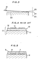
- a piezoelectric thin film 12 is first formed epitaxially on a single-crystalline dielectric member 11 by a method such as sputtering or CVD to obtain the high acoustic velocity substrate 13, and then aluminum electrodes 14 are formed on the surface of the piezoelectric thin film 12.
- the aluminum electrodes 14 are provided on the surface of the surface acoustic wave device 10 and exposed to the atmospheric air.
- a piezoelectric thin film formed by a method such as sputtering or CVD easily causes projections on its surface due to adhesion of dirt or the like. Therefore, it may not be possible to form smooth aluminum electrodes on the piezoelectric thin film.
- projections may also be formed on a photoresist film to cause difficulty in giving intimate contact of a photomask with the surface of the photoresist film, which is provided on the aluminum film, because of such projections. If the projections formed on the piezoelectric thin film cause corresponding projections on the aluminum film, further, uniform application of the photoresist material may be prevented by such projections formed on the aluminum film. Thus, the as-formed aluminum electrodes may be short-circuited.
- a surface acoustic wave device such as a SAW filter or a SAW resonator
- aluminum electrodes are subjected to strong stress by surface acoustic waves, to cause metal migration.
- This migration which is caused by stress, is called stressmigration, to be distinguished from electromigration.
- stressmigration leads to electrical shorting and characteristic deterioration such as increase of insertion loss and reduction of the quality factor (Q) of the resonator. Occurrence of such stressmigration is facilitated as the frequency is increased, to cause a significant problem particularly in a surface acoustic wave device which is employed in a high-frequency region.
- the inventors have further investigated the cause for the aforementioned stressmigration.
- the aluminum film formed by electron beam deposition, sputtering or the like for providing electrodes is not crystallographically oriented in a constant direction but remains in an amorphous polycrystalline state. This is regarded as the cause for stressmigration due to intercrystalline diffusion in such aluminum electrodes.
- an object of the present invention is to provide a surface acoustic wave device comprising aluminum electrodes, which hardly cause stressmigration and can be formed with application of photolithography with no problem.
- the present invention is directed to a surface acoustic wave device which comprises a single-crystalline dielectric member, a piezoelectric thin film epitaxially grown thereon and electrodes defining a transducer, for example.
- the inventive surface acoustic wave device is characterized in that the electrodes are formed along the interface between the dielectric member and the piezoelectric thin film and include an aluminum film which is crystallographically oriented in a constant direction.
- the aluminum electrodes are so crystallographically oriented in a constant direction, i.e., epitaxially grown, that the piezoelectric thin film can be further epitaxially grown on the single-crystalline dielectric member and on such aluminum electrodes formed on the single-crystalline dielectric member.
- the aluminum electrodes are directly formed on the surface of the single-crystalline dielectric member, and hence an aluminum film for providing the aluminum electrodes can be smoothed by specularly polishing the surface of the single-crystalline dielectric member. Therefore, the aforementioned problem in photolithography caused in formation of the aluminum film on the piezoelectric thin film is effectively solved in order to avoid inconvenience such as short-circuiting across the as-formed electrodes.
- an aluminum film whose crystal axes are oriented in a constant direction is considered to exhibit properties which are close to those of a single-crystalline film.
- such an aluminum film hardly causes stressmigration. According to the present invention, therefore, it is possible to prevent electrical shorting and increase in insertion loss caused by stressmigration.
- the present invention When the present invention is applied to a resonator, its quality factor can be prevented from reduction caused by stressmigration.
- stressmigration is facilitated as the frequency is increased.
- occurrence of such stressmigration can be suppressed according to the present invention, whereby the surface acoustic wave device can be maintained in good high-frequency characteristics while features of the high SAW velocity substrate can be sufficiently effectuated.
- the inventive surface acoustic wave device is practically applicable to a circuit, such as a transmission filter, for example, having a high signal level.
- the single-crystalline dielectric member is preferably prepared from silicon, sapphire, diamond or quartz crystal.
- the piezoelectric thin film is preferably prepared from zinc oxide or aluminum nitride.
- the single-crystalline dielectric member is prepared from sapphire
- the piezoelectric thin film is prepared from zinc oxide
- the aluminum film is prepared from a (311) plane oriented film.
- an admixture such as Cu, Ti, Ni, Mg or Pd
- the amount of such an admixture is preferably selected within a range of 0.1 to 10 percent by weight.
- a surface acoustic wave device 1 comprises a substrate 4, which is formed by a single-crystalline dielectric member 2 and a piezoelectric thin film 3 epitaxially grown on its surface.
- the single-crystalline dielectric member 2 is prepared from R-plane sapphire, for example.
- the piezoelectric thin film 3 is formed by a (1120) plane oriented thin film of ZnO, for example.
- Aluminum electrodes 5 for serving as interdigital electrodes are formed along the interface between the single-crystalline dielectric member 2 and the piezoelectric thin film 3.
- the aluminum electrodes 5 define a transducer, for example.
- an R-plane sapphire plate having a specularly polished surface was prepared for forming the single-crystalline dielectric member 2, and a thin aluminum film for providing the aluminum electrodes 5 was formed on its surface by vapor deposition. It was possible to epitaxially grow the aluminum film on the R-plane sapphire plate by controlling deposition conditions. The thickness of the as-formed aluminum film was 500 ⁇ .
- the aluminum film thus formed on the R-plane sapphire plate was analyzed through RHEED (reflection high-energy electron diffraction).
- RHEED was carried out by applying a high-energy electron beam 21 onto a surface 22 of the sample at an extremely small angle of incidence, to analyze the crystal structure of the surface 22 and a portion close thereto from the status of reflection.
- a spot-type RHEED image generally appears if the surface of a sample has a periodic crystal structure.
- a ring-shaped RHEED image appears when the surface of the sample has a polycrystalline structure, while a halo-shaped RHEED image appears when the sample surface has an amorphous structure.
- Fig. 2A shows a photograph of the aluminum film, which was formed on the R-plane sapphire plate in the aforementioned manner, taken through RHEED, and Fig. 2B is an explanatory diagram for the photograph shown in Fig. 2A.
- the wavelength of the electron beam 21 was 0.0251 ⁇ .
- the direct spot 24 of the electron beam 21 appears on a lower portion of the surface 22 of the sample (aluminum film), and the RHEED image 25 appears on an upper portion of the surface 22.
- some spots appear in the RHEED image 25, to prove that the as-formed aluminum film was epitaxially grown.
- the surface of the R-plane sapphire plate ( ⁇ -Al2O3) was a (01 1 2) plane and surface waves were propagated in a [0 1 11] direction on this (01 1 2) plane, while it has been recognized by RHEED analysis that the aluminum film was epitaxially grown on a (311) plane and surface waves were propagated in a [101 1 ] direction on the (311) oriented plane.
- interdigital aluminum electrodes 5 whose electrode fingers had widths and spaces of 1 ⁇ m on the surface of the R-plane sapphire plate.
- a ZnO film for defining the piezoelectric thin film 3 was epitaxially grown by planar magnetron sputtering on the surface, including the aluminum electrodes 5, of the single-crystalline dielectric member 2 of the R-plane sapphire plate, as shown in Fig. 1.
- the surface acoustic wave device 1 was obtained.
- the aluminum electrodes 5 were the so-called split electrodes, and the wavelength of surface acoustic waves was 8 ⁇ m.
- the thickness of the ZnO film 3 was made 0.25 times the wavelength of the Sezawa wave having a relatively large electromechanical coupling factor, i.e., 2 ⁇ m.
- the aluminum film for defining the aluminum electrodes 5 was formed on the surface of the single-crystalline dielectric member 2 made of the sapphire plate whose surface was specularly polished, whereby it was possible to smooth the aluminum film in order to prevent occurrence of a failure caused by a defect possibly resulting from photolithography.
- the aluminum film for defining the aluminum electrodes 14 is formed on the ZnO film 12 which is epitaxially grown on the R-plane sapphire plate, and photolithography is applied to this aluminum film. Therefore, projections formed on the ZnO film 12 exert such bad influence on the aluminum film that aluminum electrodes 14 experimentally obtained by photoetching were short-circuited in about 30 % of samples of the conventional surface acoustic wave device.
- Fig. 5 shows a surface acoustic wave device according to reference example, which is of interest to the present invention. If aluminum electrodes 7 formed on an R-plane sapphire plate 6 are random-oriented polycrystalline aluminum films, a ZnO film 9 cannot be epitaxially grown but remains in a polycrystalline state on regions 8 above the aluminum electrodes 7. In an experimental sample of such reference example, therefore, propagation loss was increased to at least 10 times as compared with the aforementioned embodiment.
- the aluminum electrodes 5 are provided by the epitaxially grown aluminum film, whereby it is possible to suppress occurrence of stressmigration caused by intercrystalline diffusion.
- the amount of such an admixture must be at least 0.1 percent by weight since no substantial effect is attained if the amount is too small, and is preferably not more than 10 percent by weight since resistivity of the aluminum film is increased if the amount is too large.
- the aluminum electrodes 5, which are formed along the interface between the single-crystalline dielectric member 2 and the piezoelectric thin film 3, are not exposed to the exterior and can be prevented from oxidation.
Landscapes
- Physics & Mathematics (AREA)
- Acoustics & Sound (AREA)
- Engineering & Computer Science (AREA)
- Manufacturing & Machinery (AREA)
- Surface Acoustic Wave Elements And Circuit Networks Thereof (AREA)
Applications Claiming Priority (2)
| Application Number | Priority Date | Filing Date | Title |
|---|---|---|---|
| JP174763/89 | 1989-07-06 | ||
| JP1174763A JPH0340510A (ja) | 1989-07-06 | 1989-07-06 | 弾性表面波装置 |
Publications (3)
| Publication Number | Publication Date |
|---|---|
| EP0407163A2 true EP0407163A2 (de) | 1991-01-09 |
| EP0407163A3 EP0407163A3 (en) | 1991-07-17 |
| EP0407163B1 EP0407163B1 (de) | 1995-11-22 |
Family
ID=15984245
Family Applications (1)
| Application Number | Title | Priority Date | Filing Date |
|---|---|---|---|
| EP90307292A Expired - Lifetime EP0407163B1 (de) | 1989-07-06 | 1990-07-04 | Akustische Oberflächenwellenanordnung |
Country Status (7)
| Country | Link |
|---|---|
| US (1) | US5061870A (de) |
| EP (1) | EP0407163B1 (de) |
| JP (1) | JPH0340510A (de) |
| KR (1) | KR930007797B1 (de) |
| CN (1) | CN1015041B (de) |
| CA (1) | CA2020411C (de) |
| DE (1) | DE69023707T2 (de) |
Cited By (5)
| Publication number | Priority date | Publication date | Assignee | Title |
|---|---|---|---|---|
| EP0534354A1 (de) * | 1991-09-25 | 1993-03-31 | Sumitomo Electric Industries, Limited | Akustische Oberflächenwellenanordnung und ihr Herstellungsverfahren |
| EP0587068A1 (de) * | 1992-09-11 | 1994-03-16 | Sumitomo Electric Industries, Ltd. | Akustische Oberflächenwellenanordnung und Verfahren zur Herstellung |
| EP0635938A1 (de) * | 1993-07-20 | 1995-01-25 | AVL Gesellschaft für Verbrennungskraftmaschinen und Messtechnik mbH.Prof.Dr.Dr.h.c. Hans List | Piezoelektrisches Kristallelement |
| EP0731558A1 (de) * | 1995-03-06 | 1996-09-11 | Matsushita Electric Industrial Co., Ltd. | Akustisches Oberflächenwellenmodul und Verfahren zu seiner Herstellung |
| EP1499019A1 (de) * | 2003-07-17 | 2005-01-19 | TDK Corporation | Oberflächenbauelement, Oberflächenwellenvorrichtung, Oberflächenwellenduplexer und Methode zur Herstellung eines Oberflächenbauelementes |
Families Citing this family (21)
| Publication number | Priority date | Publication date | Assignee | Title |
|---|---|---|---|---|
| US5162690A (en) * | 1989-04-14 | 1992-11-10 | Murata Manufacturing Co., Ltd. | Surface acoustic wave device |
| JPH04358410A (ja) * | 1991-06-05 | 1992-12-11 | Sumitomo Electric Ind Ltd | 表面弾性波素子及びその製造方法 |
| JPH0590871A (ja) * | 1991-09-27 | 1993-04-09 | Sumitomo Electric Ind Ltd | 表面弾性波素子 |
| US5440189A (en) * | 1991-09-30 | 1995-08-08 | Sumitomo Electric Industries, Ltd. | Surface acoustic wave device |
| JP3198691B2 (ja) * | 1993-01-14 | 2001-08-13 | 株式会社村田製作所 | 酸化亜鉛圧電結晶膜 |
| JP3085043B2 (ja) * | 1993-08-05 | 2000-09-04 | 株式会社村田製作所 | サファイア面上の酸化亜鉛圧電結晶膜 |
| KR0171921B1 (ko) * | 1993-09-13 | 1999-03-30 | 모리시타 요이찌 | 전자부품과 그 제조방법 |
| JP3295921B2 (ja) * | 1994-06-20 | 2002-06-24 | 住友電気工業株式会社 | 表面弾性波素子用ダイヤモンド基材及び素子 |
| US5633616A (en) * | 1994-10-07 | 1997-05-27 | Mitsubishi Denki Kabushiki Kaisha | Thin film saw filter including doped electrodes |
| US5576589A (en) * | 1994-10-13 | 1996-11-19 | Kobe Steel Usa, Inc. | Diamond surface acoustic wave devices |
| DE19610806A1 (de) * | 1995-03-20 | 1996-10-10 | Hitachi Media Electron Kk | Oberflächenwellen-Filter und Antennenweiche |
| US5834877A (en) * | 1995-08-28 | 1998-11-10 | Accuweb, Inc. | Ultrasonic transducer units for web detection and the like |
| JPH09223943A (ja) * | 1996-02-19 | 1997-08-26 | Nec Corp | 弾性表面波デバイス |
| KR100455493B1 (ko) * | 1998-10-16 | 2004-11-08 | 세이코 엡슨 가부시키가이샤 | 탄성 표면파 소자 |
| JP4502553B2 (ja) * | 2000-12-05 | 2010-07-14 | 日本碍子株式会社 | 弾性表面波デバイス用基板の製造方法 |
| JP2003037467A (ja) * | 2001-07-24 | 2003-02-07 | Murata Mfg Co Ltd | 弾性表面波装置 |
| TWI282660B (en) | 2001-12-27 | 2007-06-11 | Murata Manufacturing Co | Surface acoustic wave device and manufacturing method therefor |
| KR101644165B1 (ko) * | 2009-09-25 | 2016-07-29 | 삼성전자주식회사 | 표면탄성파 디바이스 및 바이오센서 |
| JP2011139214A (ja) * | 2009-12-28 | 2011-07-14 | Seiko Epson Corp | 弾性表面波デバイス、発振器、モジュール装置 |
| JP6205937B2 (ja) * | 2013-07-22 | 2017-10-04 | セイコーエプソン株式会社 | 圧電膜製造方法、振動子製造方法、振動片、振動子、発振器、電子機器及び移動体 |
| JP2020092321A (ja) | 2018-12-05 | 2020-06-11 | 太陽誘電株式会社 | 弾性波デバイスおよびその製造方法、フィルタ並びにマルチプレクサ |
Family Cites Families (14)
| Publication number | Priority date | Publication date | Assignee | Title |
|---|---|---|---|---|
| JPS5549014A (en) * | 1978-10-04 | 1980-04-08 | Seiko Instr & Electronics Ltd | Electrode for vibrating element |
| JPS5748820A (en) * | 1980-09-05 | 1982-03-20 | Murata Mfg Co Ltd | Surface acoustic wave element |
| JPS57145419A (en) * | 1981-03-05 | 1982-09-08 | Clarion Co Ltd | Surface acoustic wave element |
| DE3308365A1 (de) * | 1982-03-11 | 1983-09-15 | Nobuo Mikoshiba | Akustische oberflaechenwellen bildende vorrichtung |
| GB2181917B (en) * | 1982-03-11 | 1987-11-18 | Nobuo Mikoshiba | Surface acoustic wave device |
| JPS59231911A (ja) * | 1983-06-14 | 1984-12-26 | Clarion Co Ltd | 表面弾性波素子 |
| JPS6046108A (ja) * | 1983-08-23 | 1985-03-12 | Oki Electric Ind Co Ltd | 表面弾性波デバイスの製造方法 |
| JPS6192022A (ja) * | 1984-10-11 | 1986-05-10 | Matsushita Electric Ind Co Ltd | 表面波フイルタ |
| JPS6298812A (ja) * | 1985-10-25 | 1987-05-08 | Hitachi Ltd | 弾性表面波装置 |
| JPS62272610A (ja) * | 1986-05-21 | 1987-11-26 | Hitachi Ltd | 弾性表面波素子 |
| JPS63314906A (ja) * | 1987-06-18 | 1988-12-22 | Matsushita Electric Ind Co Ltd | 表面弾性波装置の製造方法 |
| US4935658A (en) * | 1987-10-02 | 1990-06-19 | Quartztronics, Inc. | Crystal resonator with low acceleration sensitivity and method of manufacture thereof |
| JPH01303910A (ja) * | 1988-06-01 | 1989-12-07 | Hitachi Ltd | 固体電子素子、その製造方法、及びそれを利用した装置 |
| US4968954A (en) * | 1988-09-30 | 1990-11-06 | Shin-Etsu Chemical Co., Ltd. | Epitaxial layer-bearing wafer of rare earth gallium garnet for MSW device |
-
1989
- 1989-07-06 JP JP1174763A patent/JPH0340510A/ja active Pending
-
1990
- 1990-07-04 DE DE69023707T patent/DE69023707T2/de not_active Expired - Lifetime
- 1990-07-04 EP EP90307292A patent/EP0407163B1/de not_active Expired - Lifetime
- 1990-07-04 CA CA002020411A patent/CA2020411C/en not_active Expired - Lifetime
- 1990-07-05 KR KR1019900010128A patent/KR930007797B1/ko not_active Expired - Lifetime
- 1990-07-06 CN CN90103485A patent/CN1015041B/zh not_active Expired
- 1990-07-06 US US07/549,214 patent/US5061870A/en not_active Expired - Lifetime
Cited By (12)
| Publication number | Priority date | Publication date | Assignee | Title |
|---|---|---|---|---|
| EP0534354A1 (de) * | 1991-09-25 | 1993-03-31 | Sumitomo Electric Industries, Limited | Akustische Oberflächenwellenanordnung und ihr Herstellungsverfahren |
| US5401544A (en) * | 1991-09-25 | 1995-03-28 | Sumitomo Electric Industries, Ltd. | Method for manufacturing a surface acoustic wave device |
| EP0587068A1 (de) * | 1992-09-11 | 1994-03-16 | Sumitomo Electric Industries, Ltd. | Akustische Oberflächenwellenanordnung und Verfahren zur Herstellung |
| US5343107A (en) * | 1992-09-11 | 1994-08-30 | Sumitomo Electric Industries, Ltd. | Surface acoustic wave element and method of manufacturing the same |
| US5497726A (en) * | 1992-09-11 | 1996-03-12 | Sumitomo Electric Industries, Ltd. | Method of manufacturing a surface acoustic wave element |
| EP0635938A1 (de) * | 1993-07-20 | 1995-01-25 | AVL Gesellschaft für Verbrennungskraftmaschinen und Messtechnik mbH.Prof.Dr.Dr.h.c. Hans List | Piezoelektrisches Kristallelement |
| EP0731558A1 (de) * | 1995-03-06 | 1996-09-11 | Matsushita Electric Industrial Co., Ltd. | Akustisches Oberflächenwellenmodul und Verfahren zu seiner Herstellung |
| US5757250A (en) * | 1995-03-06 | 1998-05-26 | Matsushita Electric Industrial Co., Ltd. | Surface acoustic wave module with thin film for wave transmission velocity differentiation |
| US5815900A (en) * | 1995-03-06 | 1998-10-06 | Matsushita Electric Industrial Co., Ltd. | Method of manufacturing a surface acoustic wave module |
| US5996199A (en) * | 1995-03-06 | 1999-12-07 | Matsushita Electric Industrial Co., Ltd. | Method of manufacturing surface acoustic ware modules |
| EP1499019A1 (de) * | 2003-07-17 | 2005-01-19 | TDK Corporation | Oberflächenbauelement, Oberflächenwellenvorrichtung, Oberflächenwellenduplexer und Methode zur Herstellung eines Oberflächenbauelementes |
| US7352114B2 (en) | 2003-07-17 | 2008-04-01 | Tdk Corporation | Surface acoustic wave element, surface acoustic wave device, surface acoustic wave duplexer, and method of manufacturing surface acoustic wave element |
Also Published As
| Publication number | Publication date |
|---|---|
| CA2020411C (en) | 1994-05-03 |
| EP0407163B1 (de) | 1995-11-22 |
| EP0407163A3 (en) | 1991-07-17 |
| JPH0340510A (ja) | 1991-02-21 |
| CA2020411A1 (en) | 1991-01-07 |
| DE69023707D1 (de) | 1996-01-04 |
| CN1015041B (zh) | 1991-12-04 |
| KR930007797B1 (ko) | 1993-08-19 |
| DE69023707T2 (de) | 1996-05-09 |
| US5061870A (en) | 1991-10-29 |
| KR910003921A (ko) | 1991-02-28 |
| CN1048636A (zh) | 1991-01-16 |
Similar Documents
| Publication | Publication Date | Title |
|---|---|---|
| EP0407163B1 (de) | Akustische Oberflächenwellenanordnung | |
| EP0392879B1 (de) | Akustische Oberflächenwellenanordnung | |
| US4449107A (en) | Surface elastic wave element | |
| CN1205744C (zh) | 声表面波器件及其制造工艺 | |
| EP1111779B1 (de) | Oberflächenwellenanordnung | |
| US6239536B1 (en) | Encapsulated thin-film resonator and fabrication method | |
| EP0353073A2 (de) | Akustische Oberflächenwellenanordnungen | |
| CA2197829C (en) | Surface acoustic wave device | |
| EP0657998B1 (de) | Verfahren zur Herstellung einer Elektrode für akustische Oberflächenwellenanordnung | |
| EP0534355B1 (de) | Herstellungsverfahren für akustische Oberflächenwellenanordnungen | |
| US5152864A (en) | Method of manufacturing surface acoustic wave device | |
| US4480209A (en) | Surface acoustic wave device having a specified crystalline orientation | |
| US20250351730A1 (en) | Method for manufacturing piezoelectric film, piezoelectric film manufactured by the method, and piezoelectric device | |
| Kadota et al. | Shear bulk wave transducer made of (1120)-plane epitaxial ZnO film on R-sapphire | |
| JP2545983B2 (ja) | 弾性表面波装置 | |
| US5038068A (en) | Thin film pattern and method of forming the same | |
| KR20020074484A (ko) | 탄성파 장치 | |
| JP7793785B2 (ja) | 弾性波装置、通信装置、および製造方法 | |
| JPH025331B2 (de) | ||
| JPH08148966A (ja) | 弾性表面波素子電極 | |
| JPH10135773A (ja) | 弾性表面波装置ならびにその製造方法 | |
| JPH1093368A (ja) | 弾性表面波装置の製造方法 | |
| JPH08130435A (ja) | 弾性表面波装置およびその製造方法 | |
| JPH07307634A (ja) | 弾性表面波素子電極の製造方法 | |
| JPH07326942A (ja) | 弾性表面波装置 |
Legal Events
| Date | Code | Title | Description |
|---|---|---|---|
| PUAI | Public reference made under article 153(3) epc to a published international application that has entered the european phase |
Free format text: ORIGINAL CODE: 0009012 |
|
| AK | Designated contracting states |
Kind code of ref document: A2 Designated state(s): DE FR GB |
|
| 17P | Request for examination filed |
Effective date: 19901219 |
|
| PUAL | Search report despatched |
Free format text: ORIGINAL CODE: 0009013 |
|
| AK | Designated contracting states |
Kind code of ref document: A3 Designated state(s): DE FR GB |
|
| 17Q | First examination report despatched |
Effective date: 19931129 |
|
| GRAA | (expected) grant |
Free format text: ORIGINAL CODE: 0009210 |
|
| AK | Designated contracting states |
Kind code of ref document: B1 Designated state(s): DE FR GB |
|
| REF | Corresponds to: |
Ref document number: 69023707 Country of ref document: DE Date of ref document: 19960104 |
|
| ET | Fr: translation filed | ||
| PLBE | No opposition filed within time limit |
Free format text: ORIGINAL CODE: 0009261 |
|
| STAA | Information on the status of an ep patent application or granted ep patent |
Free format text: STATUS: NO OPPOSITION FILED WITHIN TIME LIMIT |
|
| 26N | No opposition filed | ||
| REG | Reference to a national code |
Ref country code: GB Ref legal event code: IF02 |
|
| PGFP | Annual fee paid to national office [announced via postgrant information from national office to epo] |
Ref country code: FR Payment date: 20090710 Year of fee payment: 20 |
|
| PGFP | Annual fee paid to national office [announced via postgrant information from national office to epo] |
Ref country code: GB Payment date: 20090701 Year of fee payment: 20 Ref country code: DE Payment date: 20090702 Year of fee payment: 20 |
|
| REG | Reference to a national code |
Ref country code: GB Ref legal event code: PE20 Expiry date: 20100703 |
|
| PG25 | Lapsed in a contracting state [announced via postgrant information from national office to epo] |
Ref country code: GB Free format text: LAPSE BECAUSE OF EXPIRATION OF PROTECTION Effective date: 20100703 |
|
| PG25 | Lapsed in a contracting state [announced via postgrant information from national office to epo] |
Ref country code: DE Free format text: LAPSE BECAUSE OF EXPIRATION OF PROTECTION Effective date: 20100704 |