EP0407778B1 - Amplificateur hybride - Google Patents
Amplificateur hybride Download PDFInfo
- Publication number
- EP0407778B1 EP0407778B1 EP90111748A EP90111748A EP0407778B1 EP 0407778 B1 EP0407778 B1 EP 0407778B1 EP 90111748 A EP90111748 A EP 90111748A EP 90111748 A EP90111748 A EP 90111748A EP 0407778 B1 EP0407778 B1 EP 0407778B1
- Authority
- EP
- European Patent Office
- Prior art keywords
- amplifier
- metal region
- coupled
- amplifying means
- metal
- Prior art date
- Legal status (The legal status is an assumption and is not a legal conclusion. Google has not performed a legal analysis and makes no representation as to the accuracy of the status listed.)
- Expired - Lifetime
Links
Images



Classifications
-
- H—ELECTRICITY
- H03—ELECTRONIC CIRCUITRY
- H03F—AMPLIFIERS
- H03F1/00—Details of amplifiers with only discharge tubes, only semiconductor devices or only unspecified devices as amplifying elements
- H03F1/08—Modifications of amplifiers to reduce detrimental influences of internal impedances of amplifying elements
- H03F1/22—Modifications of amplifiers to reduce detrimental influences of internal impedances of amplifying elements by use of cascode coupling, i.e. earthed cathode or emitter stage followed by earthed grid or base stage respectively
-
- H—ELECTRICITY
- H03—ELECTRONIC CIRCUITRY
- H03F—AMPLIFIERS
- H03F3/00—Amplifiers with only discharge tubes or only semiconductor devices as amplifying elements
- H03F3/189—High-frequency amplifiers, e.g. radio frequency amplifiers
- H03F3/19—High-frequency amplifiers, e.g. radio frequency amplifiers with semiconductor devices only
-
- H—ELECTRICITY
- H10—SEMICONDUCTOR DEVICES; ELECTRIC SOLID-STATE DEVICES NOT OTHERWISE PROVIDED FOR
- H10W—GENERIC PACKAGES, INTERCONNECTIONS, CONNECTORS OR OTHER CONSTRUCTIONAL DETAILS OF DEVICES COVERED BY CLASS H10
- H10W44/00—Electrical arrangements for controlling or matching impedance
- H10W44/20—Electrical arrangements for controlling or matching impedance at high-frequency [HF] or radio frequency [RF]
-
- H—ELECTRICITY
- H05—ELECTRIC TECHNIQUES NOT OTHERWISE PROVIDED FOR
- H05K—PRINTED CIRCUITS; CASINGS OR CONSTRUCTIONAL DETAILS OF ELECTRIC APPARATUS; MANUFACTURE OF ASSEMBLAGES OF ELECTRICAL COMPONENTS
- H05K1/00—Printed circuits
- H05K1/02—Details
- H05K1/0213—Electrical arrangements not otherwise provided for
- H05K1/0237—High frequency adaptations
-
- H—ELECTRICITY
- H05—ELECTRIC TECHNIQUES NOT OTHERWISE PROVIDED FOR
- H05K—PRINTED CIRCUITS; CASINGS OR CONSTRUCTIONAL DETAILS OF ELECTRIC APPARATUS; MANUFACTURE OF ASSEMBLAGES OF ELECTRICAL COMPONENTS
- H05K1/00—Printed circuits
- H05K1/18—Printed circuits structurally associated with non-printed electric components
- H05K1/181—Printed circuits structurally associated with non-printed electric components associated with surface mounted components
-
- H—ELECTRICITY
- H10—SEMICONDUCTOR DEVICES; ELECTRIC SOLID-STATE DEVICES NOT OTHERWISE PROVIDED FOR
- H10W—GENERIC PACKAGES, INTERCONNECTIONS, CONNECTORS OR OTHER CONSTRUCTIONAL DETAILS OF DEVICES COVERED BY CLASS H10
- H10W44/00—Electrical arrangements for controlling or matching impedance
- H10W44/20—Electrical arrangements for controlling or matching impedance at high-frequency [HF] or radio frequency [RF]
- H10W44/226—Electrical arrangements for controlling or matching impedance at high-frequency [HF] or radio frequency [RF] for HF amplifiers
Definitions
- This invention concerns electronic assemblies and, more particularly, hybrid amplifiers for operation at radio frequencies.
- Ceramics such as for example alumina or beryllia, are much used for circuit boards because of their dimensional stability and excellent thermal properties.
- Metal film conductors prepared by means well known in the art are used on circuit boards to provide interconnections and bonding pads for various components. Some components, as for example resistors, are also provided in film form on ceramic boards. Other components, as for example, IC's, transistors, diodes, capacitors and transformers are often provided in discrete form and mounted on and/or connected to metallized contact regions on the board. Methods for providing such are well known in the art.
- a particular problem associated with electronic circuits and assemblies that must operate in the radio frequency (RF) range of 100-1000 MHz or higher is that the performance of such units is especially sensitive to parasitic R, C and L associated with the placement of the components and interconnections on the circuit board. Parasitics can adversely affect gain, bandwidth, stability and noise. Because of these parasitics, the performance of such circuits is less than ideal and there is a continuing need to provide RF circuits and assemblies, particularly hybrid RF amplifiers, in which the adverse affects of parasitics are reduced and improved performance obtained.
- US Patent No. 3,838,443 describes a low-cost mounting assembly arranged in minimise package parasitics.
- US Patent No. 4,783,697 assigned to the same assignee as the present invention, the structure of a leadless chip carrier assembly, suitable for use with radio frequency power transistors, is disclosed.
- UK Patent Application No. 2 075 298 relates to the field of high voltage, high frequency amplifiers.
- a Radio Frequency (RF) amplifier arranged on a circuit board having thereon conductors and film resistors, having: first and second amplifying means each including at least first and second directly coupled amplifier elements having first and second current electrodes and a control electrode; and first, second, third, fourth and fifth metal regions; said third and fourth metal regions having portions that extend at least partially along three sides of said first and second metal regions, respectively; wherein said first and second amplifier elements are respectively mounted on said first and second metal regions; wherein the control electrode of said first amplifier element is coupled to said fifth metal region; said first current electrode of said first amplifier element is double-bonded to said third metal region across said first metal region; said second current electrode of said first amplifier element is coupled to said first metal region; the control electrode of said second amplifier element is double-bonded to said fourth metal region across said second metal region; the first current electrode of the second amplifier element is coupled to the second current electrode of said first amplifier element; and the second current electrode of said second amplifier element is coupled to said second metal region; where
- the at least two film resistors in each amplifying means are arranged such that, during operation, current flow therethrough is substantially parallel to the first direction.
- the transverse-oriented common conductors of each amplifying means may be separated by a gap, and may also be aligned.
- aligned transverse-oriented common conductors are coupled to a ground conductor of the amplifier by a common connection, thereby eliminating asymmetric return current flow in the ground conductor and further improving balance between said first and second circuit portions.
- Each amplifying means may comprise a further film resistor having a longitudinal direction oriented transverse to the first direction, wherein the arrangement of said further film resistors is symmetrical about the first direction.
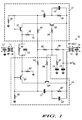
- FIG. 1 is a diagram of circuit 10 of a dual RF Cascode amplifier according to the prior art.
- circuit 10 is highly simplified in that it does not show the R, C and/or L parasitics that are present in any physical implementation of circuit 10. Theses parasitics can have a profound influence on the actual circuit performance, especially at high frequencies.
- Circuit 10 comprises two substantially identical push-pull circuit portions 12, 14, indicated by the dashed lines in FIG. 1.
- Each circuit portion 12, 14 contains substantially similar components interconnected in the same way and comprising, resistors R1-5, R1′-5′, capacitors C1-C2, C1′-C2′ and amplifying means Q1-Q2, Q1′-Q2′.
- Circuit portions 12, 14 are supplied in a push-pull fashion by RF input transformer T1 and the amplified signal is extracted through RF output transformer T2.
- Resistor R6 and capacitor C3 through the effect of a virtual ground provide a means of independently controlling the AC emitter impedance of Q1, Q1′ with no effect on the DC emitter impedance.
- DC power (Vcc) is supplied to circuit 10 through resistors R7, R8 and T2.
- Capacitor C5 is an RF by-pass capacitor. Resistor R9 and capacitor C4 are optional.
- Optional output shunt capacitor C6 assists in controlling the high frequency gain and output impedance of circuit 10.
- Optional input shunt capacitor C7 assists in controlling the high frequency input impedance of circuit 10.
- Bipolar transistors are typically used for amplifying means Q1, Q2, Q1′, Q2′ because of their excellent high frequency properties but other types of RF amplifying components, IC's or sub-assemblies may also be used.
- Optional capacitors (not shown) may also be provided from the bases of Q1, Q1′ to ground to assist in input impedance matching.
- RF-MOSFETS are an example of a suitable alternative amplifying component.
- Input amplifiers Q1, Q1′ are operated in a base-input, common-emitter configuration.
- the collector-outputs of transistors Q1, Q1′ are directly connected to the emitter-inputs of Q2, Q2′, respectively, which are operated in the common-base configuration.
- the collector-outputs of Q2, Q2′ are connected to each end of the primary windings of RF output transformer T2.
- Series feedback elements R2, R2′ R6 and C3 and shunt feedback elements C1-C2, R5 and C1′-C2′, R5′ assist in stabilizing the amplifier and reducing distortion, and in controlling gain and input-output impedance.
- the functions of the the other resistors and capacitors of circuit 10 are well understood in the art.
- balanced cascode amplifier circuit 10 is conceptually simple, the physical realization is quite complex where operation at very high frequencies, especially RF frequencies (100-1000 MHz or more) is intended. This is because, any physical realization inevitably introduces parasitic R, C, and/or L which tend to degrade performance from the ideal represented by circuit 10. It is the management of these parasitics that determines the ultimate performance of the physical circuit. These parasitics are primarily determined by the layout of the components and interconnections on the circuit board.
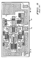
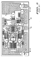
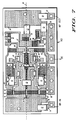
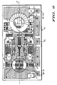
- FIGS. 2-5 show simplified plan views of prior art circuit board 20 on which circuit 10 is implemented at various stages of manufacture and FIGS. 6-9 show analogous circuit board 40 implementing circuit 10 according to the present invention.
- Circuit boards 20, 40 measure approximately 13 x 25 mm in area.
- FIGS. 2-9 metal bonding and interconnection regions are shown as light grey or lightly stippled regions and film resistors are shown as darker grey or more heavily stippled regions.
- the same designators e.g., R1-R9, C1-C6 and Q1-Q2 (primed and un-primed) have been used on FIGS. 2-9 as on circuit 10 of FIG. 1.
- the letters "G" on FIGS. 2-9 indicate various ground (i.e., common return) regions.
- each region of boards 20 or 40 may be related to the corresponding component or connection of circuit 10.
- FIG. 2 is a simplified plan view of circuit board 20 with metal regions and film resistors provided thereon. Methods for fabricating such boards with patterned metallization and film resistors are well known in the art. Either thick or thin film fabrication technologies may be employed.
- FIG. 3 shows the same board as in FIG. 2 but with the chip capacitors C1-C6, C1′-C6′ and bipolar transistors Q1,Q2, Q1′,Q2′ added. These are typically soldered in place but any convenient attachment method consistent with the electrical and thermal requirements may be used. Such methods are well known in the art.
- FIG. 4 shows the same board as in FIG. 3 but with various additional interconnections provided, as for example, by wire bonding.
- wire bonding As those of skill in the art will appreciate, certain of the wire bonded connections are discretionary, as for example, those bridging across various portions of R7 or R8 so as to permit adjustment of their resistances or C2, C2′ to permit adjustment of their capacitances.
- FIG. 5 shows the same board as in FIG. 4 but with transformers T1, T2 added. The circuit is now complete.
- metal region 21 is provided for mounting the collector of transistor Q1 and providing a bonding location for connecting the collector of Q1 to the emitter of Q2.
- Metal region 22 is provided for mounting the collector of transistor Q2, for providing a terminus for resistor R5 and for providing a terminus for bonding to capacitor C2.
- Capacitor C2 is formed by the side-by-side interrupted metal regions indicated at that location on board 20. The magnitude of C2 is adjusted by bonding together one or more lengths of metal (see FIG. 3). The capacitance of C2 is very small.
- Metal region 23 interconnects resistors R1 and R3, provides one terminus for capacitor C1 and provides a terminus for wire bonding to the base of transistor Q1.
- Metal region 24 provides a terminus of resistor R2 and a bonding location for bonding to the emitter of Q1, and provides a terminus for resistor R6 and capacitor C3.
- Metal region 25 provides a terminus for resistor R4 and a bonding location for bonding to the base of Q2.
- Metal region 26 provides the other plate of the side-by-side metal regions forming capacitor C2 and provides the other terminus for capacitor C1.
- Metal region 27 provides the other terminus for resistor R4 and a terminus for resistors R7-R9.
- Metal region 28 interconnects resistors R3 and R7.
- Metal region 29 connects resistors R8 to Vcc.
- Metal regions 30 are ground (i.e., common return) connections.
- Metal regions 31, 32 provide connections for RF-IN and RF-OUT respectively and metal region 33 provides a terminus for capacitor C4 whose other terminus is connected to an adjacent ground region 30.
- the other ends of resistors R1, R2 and capacitors C4, C5 are coupled to other adjacent ground regions 30.
- primed portion 14 of the dual amplifier are indicated on FIGS. 2-5 by the same numbers with a prime symbol and, as those of skill in the art will understand, provide corresponding connections to the primed and other components.
- FIGS. 2-5 While prior art realizations of circuit 10, as exemplified by FIGS. 2-5, give good performance, further improvement is desired.
- the present invention is concerned with improving the performance primarily through re-arrangement of the physical layout of the components and connections on the circuit board. These re-arrangements also allow the magnitude of some of the components shown in circuit 10 to be adjusted to more favorable ranges, further contributing to improved performance.
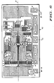
- FIGS. 6-9 show simplified plan views of an improved physical realization of circuit 10, analogous to FIGS. 2-5, but according to the present invention.
- circuit board 40 The locations of the various components on circuit board 40 have been marked in the same way as in FIGS. 2-5 to correspond to the components indicated in circuit 10.
- Metallized regions 41-53 identified in FIGS. 6-9 are analogous to metallized regions 21-33, respectively, and correspond to the same interconnections in circuit 10.
- the dimensions of circuit board 40 are the same as circuit board 20 and no additional board space is required.
- Amplifiers implementing circuit 10 were constructed according to prior art layouts and arrangements and according to the present invention shown in FIGS. 6-9. Bipolar transistor chips having f t values of at least 6 GHz were used for Q1, Q1′, Q2, Q2′. The amplifiers were tuned to operate in the range of 40-550 MHz and had nominal in-band gains of about 18 db with matched loads. Other things being equal, it was found that the improved arrangement of the present invention provided greater gain at high frequencies, e.g., at least 1 db greater at 550 MHz. This is a significant improvement.
- Gain stability describes the propensity of the amplifier to break into oscillations when, for example, the load impedance is varied. This is an important property of RF amplifiers. Typically such oscillations occur at out-of-band frequencies above the intended upper cut-off frequency of the amplifier, for example, in the range 750-1200 Mhz for a typical prior art 40-550 MHz amplifier. Such conditions are familiar to those of skill in the art and are a significant design problem in RF circuits. Absolutely stable amplifiers are much desired but have not been possible with the prior art arrangements. At certain output impedance conditions, the gain and phase shift of the prior art amplifiers are such that oscillations may occur.
- resistors R4, R4′ which have previously been required to be comparatively high (e.g., 40 ohms) to achieve adequate circuit stability could be reduced to much smaller values (e.g., 5 ohms) thereby also substantially reducing amplifier distortion.
- a composite triple beat distortion reduction of at least 1 db is obtained in this way. This is very significant.
- FIGS. 6-9 the physical arrangement of the components enclosed in the amplifier portions within dashed lines 12, 14 of FIG. 1 have been modified to provide as nearly perfect physical mirror symmetry about line 60 as possible. This more perfect mirror symmetry provides a much improved virtual ground between circuit portions 12, 14 along line 60. This greatly reduces the effect of parasitics associated with circuit portions 12, 14. Several important aspects of these changes contribute to reducing the parasitic effects.
- resistors R1, R2 (and counterparts R1′, R2′) have been reoriented so that current flow therein is substantially parallel to mirror line 60 and so that resistors R1, R2 are substantially aligned and terminate on newly provided common conductor 54 (resistors R1′, R2′ are also aligned and terminate on newly provided common conductor 54′).
- the longer dimensions of R1, R2 (and R1′, R2′) are transverse to line 60 in this example, but this depends on the desired resistance values or ratios.
- Common conductors 54, 54′ which are symmetrical about mirror line 60 and oriented transverse thereto have been added. It is desirable that common conductors 54, 54′ be separated by a gap so that the resistors and circuit portions 12, 14 can be individually tested during manufacture. Spaced-apart common conductors 54, 54′ are then joined together and to adjacent ground region 50 by conductors 55 (see FIG. 8) so that there is substantially only a single symmetric ground connection location for common conductors 54, 54′. This eliminates asymmetrical return current flow in ground region 50 near input 51 further improving the balance between circuit portions 12, 14.
- metal regions 44, 44′ and 45, 45′ have been enlarged with respect to prior art regions 24, 24′ and 25, 25′.
- metal region 44 is arranged to have a U-shaped portion that extends along three sides of metal region 41 on which Q1 is mounted so that the emitter connections to Q1 may be double bonded from opposite arms of the U. This substantially reduces the parasitic inductance and resistance of the emitter connection to Q1 and materially improves performance.
- the combination of the double bonded emitter of Q1 permitted by the U-shaped portion of metal region 44 and the double bonded base of Q2 permitted by the U-shaped portion of metal region 45 is also a new feature.
- Metal regions 44′ and 45′ have the same features, mirror symmetric about line 60.
- resistor R3 has been re-arranged to have current flow transverse to mirror line 60 and relocated so as to reduce the parasitic coupling to capacitor C2 and to provide the additional space needed for the U-shaped arms of metal region 44. Locating resistor R3 farther from capacitor C2 decouples the symmetrical amplifier circuitry from the bias chain associated with resistors R7, R8 and conductors 47, 48. This helps eliminate feedback of distortion components present on conductor 47.
- resistor R3′ and associated conductors so that the arrangement of R3, R3′ is symmetrical about line 60 and both R3, R3′ and C2, C2′ are less affected by the proximity of the non-symmetrical portions of circuit 10. This reduces the effects of the parasitics associated with these resistors, capacitors and connecting leads. In the particular embodiment shown, the longer dimensions of R3, R3′ are transverse to line 60, but this depends on the desired resistance values or ratios.
- the invented arrangement provides improved performance over the prior art, for example, greater gain-bandwidth and better gain stability margin, using substantially the same components and with the same or smaller board space. These are significant improvements which are especially valuable in connection with RF amplifiers. It will also be observed that the improved layout lends itself more readily to shrinking the overall circuit board area.
Landscapes
- Engineering & Computer Science (AREA)
- Power Engineering (AREA)
- Amplifiers (AREA)
- Structure Of Printed Boards (AREA)
- Microwave Amplifiers (AREA)
Claims (6)
- Amplificateur RF (10), disposé sur un circuit (40) présentant des conducteurs et des résistances à couche, comprenant:
un premier et un deuxième moyens d'amplification comportant chacun au moins un premier (Q1) et un deuxième (Q2) éléments amplificateurs directement couplés ayant une première et une deuxième électrodes de courant et une électrode de contrôle; et
une première (41), deuxième (42), troisième (44), quatrième (45) et cinquième (43) zones métalliques; lesdites troisième (44) et quatrième (45) zones métalliques présentant des parties qui s'étendent au moins partiellement le long de trois côtés desdites première (41) et deuxième (42) zones métalliques respectives;
dans lequel lesdits premier et deuxième éléments amplificateurs sont respectivement montés sur lesdites première (41) et deuxième (42) zones métalliques;
dans lequel l'électrode de contrôle dudit premier élément amplificateur (Q1) est couplée à ladite cinquième zone métallique (43); ladite première électrode de courant dudit premier élément amplificateur (Q1) est à double report sur ladite troisième zone métallique (44) transversalement à ladite première zone métallique (41); ladite deuxième électrode de courant dudit premier élément amplificateur (Q1) est couplée à ladite première zone métallique (41); l'électrode de contrôle dudit deuxième élément amplificateur (Q2) est à double report sur ladite quatrième zone métallique (45) transversalement à ladite deuxième zone métallique (42); la première électrode de courant du deuxième élément amplificateur (Q2) est couplée à la deuxième électrode de courant dudit premier élément amplificateur (Q1); et la deuxième électrode de courant dudit deuxième élément amplificateur (Q2) est couplée à ladite deuxième zone métallique (42);
dans lequel lesdits premier et deuxième moyens d'amplification sont disposés de manière symétrique en miroir de chaque côté d'une première direction (60) s'étendant le long du circuit (40), dans lequel au moins deux résistances à couche (R1, R2) dans chacun des moyens d'amplification ont des premières extrémités se terminant sur un conducteur commun (54), chaque conducteur commun (54) étant relié à un potentiel de la terre et orienté transversalement à la première direction (60), l'autre extrémité d'une première desdites deux résistances au moins étant couplée à ladite cinquième zone métallique (43), et l'autre extrémité d'une deuxième desdites deux résistances au moins étant couplée avec ladite troisième zone métallique (44), grâce à quoi la symétrie fournit une terre virtuelle améliorée entre les premier et deuxième moyens d'amplification, et réduit les effets des parasites. - Amplificateur selon la revendication 1, dans lequel les deux résistances au moins à couche (R1, R2) dans chaque moyen d'amplification sont disposées de manière que, pendant le fonctionnement, le flux de courant qui les traverse soit essentiellement parallèle à la première direction (60).
- Amplificateur selon la revendication 1 ou 2, dans lequel les conducteurs communs orientés transversalement (54) de chaque moyen d'amplification sont séparés par un espace (56).
- Amplificateur selon la revendication 1, 2, ou 3, dans lequel les conducteurs communs orientés transversalement (54) de chaque moyen d'amplification sont alignés.
- Amplificateur selon la revendication 4, dans lequel les conducteurs communs orientés transversalement alignés (54) sont couplés à un conducteur de terre de l'amplificateur par une connexion commune (50), supprimant de ce fait le flux de courant inverse asymétrique dans le conducteur de terre, et améliorant de plus l'équilibre entre lesdites première (12) et deuxième (14) parties du circuit.
- Amplificateur selon l'une quelconque des revendications précédentes, dans lequel chaque moyen d'amplification comprend une autre résistance à couche (R3) présentant une direction longitudinale orientée transversalement à la première direction (60), dans lequel la disposition de ladite autre résistance à couche est symétrique à ladite première direction.
Applications Claiming Priority (2)
| Application Number | Priority Date | Filing Date | Title |
|---|---|---|---|
| US380230 | 1989-07-14 | ||
| US07/380,230 US4965526A (en) | 1989-07-14 | 1989-07-14 | Hybrid amplifier |
Related Child Applications (1)
| Application Number | Title | Priority Date | Filing Date |
|---|---|---|---|
| EP93116610.2 Division-Into | 1990-06-21 |
Publications (3)
| Publication Number | Publication Date |
|---|---|
| EP0407778A2 EP0407778A2 (fr) | 1991-01-16 |
| EP0407778A3 EP0407778A3 (en) | 1991-07-24 |
| EP0407778B1 true EP0407778B1 (fr) | 1995-04-05 |
Family
ID=23500401
Family Applications (1)
| Application Number | Title | Priority Date | Filing Date |
|---|---|---|---|
| EP90111748A Expired - Lifetime EP0407778B1 (fr) | 1989-07-14 | 1990-06-21 | Amplificateur hybride |
Country Status (5)
| Country | Link |
|---|---|
| US (1) | US4965526A (fr) |
| EP (1) | EP0407778B1 (fr) |
| JP (1) | JPH0352407A (fr) |
| DE (1) | DE69018326T2 (fr) |
| MY (1) | MY105947A (fr) |
Families Citing this family (8)
| Publication number | Priority date | Publication date | Assignee | Title |
|---|---|---|---|---|
| US5268549A (en) * | 1990-06-01 | 1993-12-07 | Butler William F | Method and apparatus for destroying a syringe needle |
| JPH07211856A (ja) * | 1994-01-12 | 1995-08-11 | Fujitsu Ltd | 集積回路モジュール |
| JP2853739B2 (ja) * | 1996-09-30 | 1999-02-03 | 日本電気株式会社 | 負帰還増幅回路 |
| JPH10116732A (ja) * | 1996-10-09 | 1998-05-06 | Nec Corp | 伝送線路トランス及びこれを使用した増幅ユニット |
| JPH10135749A (ja) * | 1996-10-29 | 1998-05-22 | Nec Corp | 高周波帯増幅器 |
| US6011438A (en) * | 1997-11-27 | 2000-01-04 | Nec Corporation | Push-pull wideband semiconductor amplifier |
| US20010043121A1 (en) | 1997-11-27 | 2001-11-22 | Yuji Kakuta | Semiconductor circuit with a stabilized gain slope |
| TW498602B (en) * | 2000-05-30 | 2002-08-11 | Alps Electric Co Ltd | Circuit unit |
Citations (1)
| Publication number | Priority date | Publication date | Assignee | Title |
|---|---|---|---|---|
| US4783697A (en) * | 1985-01-07 | 1988-11-08 | Motorola, Inc. | Leadless chip carrier for RF power transistors or the like |
Family Cites Families (5)
| Publication number | Priority date | Publication date | Assignee | Title |
|---|---|---|---|---|
| DE2250918C2 (de) * | 1971-10-27 | 1982-02-04 | Westinghouse Electric Corp., 15222 Pittsburgh, Pa. | Chipträger für Mikrowellen-Leistungstransistoren und Verfahren zu seiner Herstellung |
| US4001711A (en) * | 1974-08-05 | 1977-01-04 | Motorola, Inc. | Radio frequency power amplifier constructed as hybrid microelectronic unit |
| US4342967A (en) * | 1980-05-01 | 1982-08-03 | Gte Laboratories Incorporated | High voltage, high frequency amplifier |
| US4500850A (en) * | 1981-10-22 | 1985-02-19 | Robert Grodinsky | Audio amplifier apparatus with minimum non-linear distortion |
| US4465979A (en) * | 1982-10-08 | 1984-08-14 | Fred S. Eichelberger | UHF antenna amplifier having planar transformers |
-
1989
- 1989-07-14 US US07/380,230 patent/US4965526A/en not_active Expired - Lifetime
-
1990
- 1990-06-21 DE DE69018326T patent/DE69018326T2/de not_active Expired - Fee Related
- 1990-06-21 EP EP90111748A patent/EP0407778B1/fr not_active Expired - Lifetime
- 1990-07-02 JP JP2176104A patent/JPH0352407A/ja active Pending
- 1990-07-11 MY MYPI90001161A patent/MY105947A/en unknown
Patent Citations (1)
| Publication number | Priority date | Publication date | Assignee | Title |
|---|---|---|---|---|
| US4783697A (en) * | 1985-01-07 | 1988-11-08 | Motorola, Inc. | Leadless chip carrier for RF power transistors or the like |
Also Published As
| Publication number | Publication date |
|---|---|
| DE69018326T2 (de) | 1995-11-02 |
| US4965526A (en) | 1990-10-23 |
| EP0407778A3 (en) | 1991-07-24 |
| EP0407778A2 (fr) | 1991-01-16 |
| JPH0352407A (ja) | 1991-03-06 |
| MY105947A (en) | 1995-02-28 |
| DE69018326D1 (de) | 1995-05-11 |
Similar Documents
| Publication | Publication Date | Title |
|---|---|---|
| JP3208844B2 (ja) | 高周波線形増幅器アセンブリ | |
| US7061329B2 (en) | Semiconductor device having balanced circuit for use in high frequency band | |
| US6614308B2 (en) | Multi-stage, high frequency, high power signal amplifier | |
| US4595881A (en) | Distributed amplifier using dual-gate GaAs FET's | |
| JPH0831750B2 (ja) | Rf増幅器 | |
| US6169461B1 (en) | High-frequency oscillating circuit | |
| US7548118B2 (en) | Semiconductor device and power amplifier | |
| KR100335681B1 (ko) | 반도체장치 | |
| US4864250A (en) | Distributed amplifier having improved D.C. biasing and voltage standing wave ratio performance | |
| EP0407778B1 (fr) | Amplificateur hybride | |
| JPH05251963A (ja) | 高利得モノリシックマイクロ波集積回路増幅器 | |
| JPH0514069A (ja) | 高出力電界効果トランジスタ増幅器 | |
| WO2000075990A1 (fr) | Transistor de puissance rf a adaptation d'impedance elevee | |
| JP2001274639A (ja) | 半導体電力増幅器および多段モノリシック集積回路 | |
| EP0853379A1 (fr) | Amplificateur à faible bruit | |
| US6278329B1 (en) | Low-noise amplifier stage with matching network | |
| US6320468B2 (en) | Method and system for suppressing oscillations in a multi-stage amplifier | |
| EP0920730B1 (fr) | Amplificateur pour applications de reseaux de cables | |
| EP0579293A1 (fr) | Amplificateur hybride | |
| WO2002080355A1 (fr) | Amplificateur haute frequence | |
| EP0355670A2 (fr) | Amplificateur de fréquences micro-ondes à bruit bas, à gain, stabilité et commande de bruit optimaux | |
| JP2000209038A (ja) | 高周波電力増幅装置および無線通信機 | |
| JP2025186975A (ja) | 高周波増幅器 | |
| JPH06252668A (ja) | マイクロ波回路 | |
| JPH04287507A (ja) | 電界効果トランジスタ増幅器 |
Legal Events
| Date | Code | Title | Description |
|---|---|---|---|
| PUAI | Public reference made under article 153(3) epc to a published international application that has entered the european phase |
Free format text: ORIGINAL CODE: 0009012 |
|
| AK | Designated contracting states |
Kind code of ref document: A2 Designated state(s): DE FR GB IT |
|
| PUAL | Search report despatched |
Free format text: ORIGINAL CODE: 0009013 |
|
| AK | Designated contracting states |
Kind code of ref document: A3 Designated state(s): DE FR GB IT |
|
| 17P | Request for examination filed |
Effective date: 19920109 |
|
| 17Q | First examination report despatched |
Effective date: 19930517 |
|
| GRAA | (expected) grant |
Free format text: ORIGINAL CODE: 0009210 |
|
| ITF | It: translation for a ep patent filed | ||
| AK | Designated contracting states |
Kind code of ref document: B1 Designated state(s): DE FR GB IT |
|
| XX | Miscellaneous (additional remarks) |
Free format text: TEILANMELDUNG 93116610.2 EINGEREICHT AM 21/06/90. |
|
| ET | Fr: translation filed | ||
| REF | Corresponds to: |
Ref document number: 69018326 Country of ref document: DE Date of ref document: 19950511 |
|
| PLBE | No opposition filed within time limit |
Free format text: ORIGINAL CODE: 0009261 |
|
| STAA | Information on the status of an ep patent application or granted ep patent |
Free format text: STATUS: NO OPPOSITION FILED WITHIN TIME LIMIT |
|
| 26N | No opposition filed | ||
| REG | Reference to a national code |
Ref country code: GB Ref legal event code: 746 Effective date: 19990325 |
|
| PGFP | Annual fee paid to national office [announced via postgrant information from national office to epo] |
Ref country code: DE Payment date: 20000418 Year of fee payment: 11 |
|
| PGFP | Annual fee paid to national office [announced via postgrant information from national office to epo] |
Ref country code: GB Payment date: 20000502 Year of fee payment: 11 |
|
| PGFP | Annual fee paid to national office [announced via postgrant information from national office to epo] |
Ref country code: FR Payment date: 20000602 Year of fee payment: 11 |
|
| PG25 | Lapsed in a contracting state [announced via postgrant information from national office to epo] |
Ref country code: GB Free format text: LAPSE BECAUSE OF NON-PAYMENT OF DUE FEES Effective date: 20010621 |
|
| GBPC | Gb: european patent ceased through non-payment of renewal fee |
Effective date: 20010621 |
|
| PG25 | Lapsed in a contracting state [announced via postgrant information from national office to epo] |
Ref country code: FR Free format text: LAPSE BECAUSE OF NON-PAYMENT OF DUE FEES Effective date: 20020228 |
|
| PG25 | Lapsed in a contracting state [announced via postgrant information from national office to epo] |
Ref country code: DE Free format text: LAPSE BECAUSE OF NON-PAYMENT OF DUE FEES Effective date: 20020403 |
|
| REG | Reference to a national code |
Ref country code: FR Ref legal event code: D6 |
|
| PG25 | Lapsed in a contracting state [announced via postgrant information from national office to epo] |
Ref country code: IT Free format text: LAPSE BECAUSE OF NON-PAYMENT OF DUE FEES;WARNING: LAPSES OF ITALIAN PATENTS WITH EFFECTIVE DATE BEFORE 2007 MAY HAVE OCCURRED AT ANY TIME BEFORE 2007. THE CORRECT EFFECTIVE DATE MAY BE DIFFERENT FROM THE ONE RECORDED. Effective date: 20050621 |