EP0409257A2 - Dispositif semiconducteur scellé du verre à bas point de fusion et procédé de fabrication - Google Patents
Dispositif semiconducteur scellé du verre à bas point de fusion et procédé de fabrication Download PDFInfo
- Publication number
- EP0409257A2 EP0409257A2 EP90113946A EP90113946A EP0409257A2 EP 0409257 A2 EP0409257 A2 EP 0409257A2 EP 90113946 A EP90113946 A EP 90113946A EP 90113946 A EP90113946 A EP 90113946A EP 0409257 A2 EP0409257 A2 EP 0409257A2
- Authority
- EP
- European Patent Office
- Prior art keywords
- cap
- base
- semiconductor device
- melting point
- low
- Prior art date
- Legal status (The legal status is an assumption and is not a legal conclusion. Google has not performed a legal analysis and makes no representation as to the accuracy of the status listed.)
- Withdrawn
Links
Images




Classifications
-
- H—ELECTRICITY
- H10—SEMICONDUCTOR DEVICES; ELECTRIC SOLID-STATE DEVICES NOT OTHERWISE PROVIDED FOR
- H10W—GENERIC PACKAGES, INTERCONNECTIONS, CONNECTORS OR OTHER CONSTRUCTIONAL DETAILS OF DEVICES COVERED BY CLASS H10
- H10W95/00—Packaging processes not covered by the other groups of this subclass
-
- H—ELECTRICITY
- H10—SEMICONDUCTOR DEVICES; ELECTRIC SOLID-STATE DEVICES NOT OTHERWISE PROVIDED FOR
- H10W—GENERIC PACKAGES, INTERCONNECTIONS, CONNECTORS OR OTHER CONSTRUCTIONAL DETAILS OF DEVICES COVERED BY CLASS H10
- H10W70/00—Package substrates; Interposers; Redistribution layers [RDL]
- H10W70/60—Insulating or insulated package substrates; Interposers; Redistribution layers
- H10W70/67—Insulating or insulated package substrates; Interposers; Redistribution layers characterised by their insulating layers or insulating parts
- H10W70/68—Shapes or dispositions thereof
-
- H—ELECTRICITY
- H10—SEMICONDUCTOR DEVICES; ELECTRIC SOLID-STATE DEVICES NOT OTHERWISE PROVIDED FOR
- H10W—GENERIC PACKAGES, INTERCONNECTIONS, CONNECTORS OR OTHER CONSTRUCTIONAL DETAILS OF DEVICES COVERED BY CLASS H10
- H10W72/00—Interconnections or connectors in packages
- H10W72/30—Die-attach connectors
-
- H—ELECTRICITY
- H10—SEMICONDUCTOR DEVICES; ELECTRIC SOLID-STATE DEVICES NOT OTHERWISE PROVIDED FOR
- H10W—GENERIC PACKAGES, INTERCONNECTIONS, CONNECTORS OR OTHER CONSTRUCTIONAL DETAILS OF DEVICES COVERED BY CLASS H10
- H10W76/00—Containers; Fillings or auxiliary members therefor; Seals
- H10W76/60—Seals
-
- H—ELECTRICITY
- H10—SEMICONDUCTOR DEVICES; ELECTRIC SOLID-STATE DEVICES NOT OTHERWISE PROVIDED FOR
- H10W—GENERIC PACKAGES, INTERCONNECTIONS, CONNECTORS OR OTHER CONSTRUCTIONAL DETAILS OF DEVICES COVERED BY CLASS H10
- H10W72/00—Interconnections or connectors in packages
- H10W72/071—Connecting or disconnecting
- H10W72/073—Connecting or disconnecting of die-attach connectors
-
- H—ELECTRICITY
- H10—SEMICONDUCTOR DEVICES; ELECTRIC SOLID-STATE DEVICES NOT OTHERWISE PROVIDED FOR
- H10W—GENERIC PACKAGES, INTERCONNECTIONS, CONNECTORS OR OTHER CONSTRUCTIONAL DETAILS OF DEVICES COVERED BY CLASS H10
- H10W72/00—Interconnections or connectors in packages
- H10W72/071—Connecting or disconnecting
- H10W72/073—Connecting or disconnecting of die-attach connectors
- H10W72/07331—Connecting techniques
- H10W72/07337—Connecting techniques using a polymer adhesive, e.g. an adhesive based on silicone or epoxy
- H10W72/07338—Connecting techniques using a polymer adhesive, e.g. an adhesive based on silicone or epoxy hardening the adhesive by curing, e.g. thermosetting
-
- H—ELECTRICITY
- H10—SEMICONDUCTOR DEVICES; ELECTRIC SOLID-STATE DEVICES NOT OTHERWISE PROVIDED FOR
- H10W—GENERIC PACKAGES, INTERCONNECTIONS, CONNECTORS OR OTHER CONSTRUCTIONAL DETAILS OF DEVICES COVERED BY CLASS H10
- H10W72/00—Interconnections or connectors in packages
- H10W72/50—Bond wires
- H10W72/541—Dispositions of bond wires
- H10W72/5449—Dispositions of bond wires not being orthogonal to a side surface of the chip, e.g. fan-out arrangements
Definitions
- the present invention relates to a low-melting point glass sealed semiconductor device containing a semiconductor chip which is die-bonded to a ceramic substrate by use of a thermosetting mounting agent.
- a conventional low-melting point glass sealed semiconductor device comprises: a ceramic substrate 1 coated with low-melting point glass 3 and serving as a cap; and a ceramic substrate 2 coated with low-melting point glass 4 and having a chip 5 thereon.
- the substrates 1 and 2 are overlaid with each other, with their glass-coated sides overlapped, and are then subjected to heat treatment. After melted by this heat treatment, the glass coated on the substrates 1 and 2 sets or hardens, thereby sealing the chip 5 on the ceramic substrate 2.
- the conventional low-melting point glass sealed semiconductor device shown in Fig. 1 will be described in more detail.
- the semiconductor chip 5 is located on the predetermined position of the ceramic substrate 2.
- the semiconductor chip 5 is adhered to the ceramic substrate 2 by use of a thermosetting mounting agent (not shown).
- a thermosetting mounting agent (not shown).
- a polyimide-based agent is used as this thermosetting mounting agent, since it enables efficient work and provides reliable adhesion and since it is lower in price than gold paste.
- a lead frame 6 is located on low-melting point glass 4. It is electrically connected to the semiconductor chip 5 by wires 7.
- the ceramic substrate 1 serving as a cap is adhered to the other ceramic substrate 2. Between these ceramic substrates 1 and 2, the lead frame 6 is sandwiched and hermetically sealed.
- the thermosetting mounting agent used in the semiconductor device has a characteristic of decomposing into a gas at a high temperature.
- the low-melting point glass sealed semiconductor device mentioned above is manufactured as follows. First, the ceramic substrate 2 is coated with low-melting point glass 4 in a similar manner to that in a printing process, except for the portion on which the semiconductor chip 5 is to be mounted. Next, the lead frame 6 is mounted on the low-melting point glass 4, and the chip 5 is mounted on the portion which is not coated with the glass, by use of the thermosetting mounting agent. Thereafter, the lead frame 6 and the semiconductor chip 5 are electrically connected together by wires 7. Next, the low-melting point glass 3 on ceramic substrate 2 and that 4 on ceramic substrate 3 are heated at a temperature higher than their melting points. In the state where the glass is melted, the ceramic substrates 1 and 2 are overlaid with each other and hermetically sealed.
- thermosetting mounting agent it uses is likely to decompose into a gas at a high temperature. If the thermosetting mounting agent hardenes, a gas, voids are generated in the low-melting point glass 3, 4. In addition, the gas spreads along the surface of the lead frame 6, so that a tunnel-like void extending from the interior of the glass to the outside of the semiconductor device is formed, resulting in defective adhesion.
- the first object of the present invention is to provide a low-melting point glass sealed semiconductor device, which has few voids (externally-exposed ones and internal ones) in the glass portion thereof, is reliable in both sealed characteristic and operation and yet low in price, and can be manufactured at high yield.
- the second object of the present invention is to provide a method of manufacturing such a semiconductor device.
- the present invention provides a low-melting point glass sealed semiconductor device which comprises: a first ceramic substrate may be curving a plate three sides of which form a rectangle, and the fourth side of which is arcuate, around an axis parallel to one of two axes of the plate with a predetermined curvature; a semiconductor chip adhered to a central portion of an inwardly-curved surface of the first ceramic substrate by use of a polyimide-based thermosetting mounting agent; a second ceramic substrate may be curving a plate three sides of which form a rectangle, and the fourth side of which is arcuate, around an axis parallel to one of the two axes of the plate with a predetermined curvature; and a filler member including: low-melting point glass which is coated on the inwardly-curved surface of the first ceramic substrate, except for a portion to which the semiconductor chip is adhered; and low-melting point glass which is coated on an inwardly-curved surface of the second ceramic substrate; wherein the first and second ceramic substrate
- the present invention provides a method of manufacturing a low-melting point glass sealed semiconductor device, which comprises the steps of: preparing first and second ceramic substrates each of which has a rectangular shape and is curved around one of two axes thereof with a predetermined curvature; coating low-melting point glass on an inwardly-curved surface of the first ceramic substrate, except for a portion to which a semiconductor substrate is to be adhered; adhering the semiconductor substrate to a central portion of the inwardly-curved surface of the first ceramic substrate by use of a polyimide-based thermosetting mounting agent; coating low-melting point glass on an inwardly-curved surface of the second ceramic substrate; bringing straight side edges of the first and second ceramic substrates into contact with each other, with the inwardly-curved surfaces thereof facing each other; and gradually heating the first and second ceramic substrates, such that a gas generated from part of the thermosetting mounting agent is first guided to the outside of the device through a space defined between the curved ceramic substrates
- the low-melting point glass sealed semiconductor device of the present invention does not contain a void arising from a gas generated by the thermosetting mounting agent.
- the semiconductor device does not have a tunnel-like void extending along the lead frame, i.e., a a tunnel-like void extending from the interior of the glass to the outside of the semiconductor device. Therefore, the semiconductor device is reliable in its sealed characteristic.
- the gas produced by the decomposition of part of the thermosetting mounting agent escapes to the outside the device through the spaced defined between the first and second ceramic substrates. After the gas is completely expelled from the device, the low-melting point glass is melted, thereby filling the space and adhering the first and second ceramic substrates to each other.
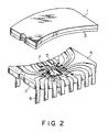
- Fig. 2 is a perspective view of the low-melting point glass sealed semiconductor device according to one embodiment of the present invention.
- a ceramic substrate 1 (which is used as a cap) and a ceramic substrate 2 (on which a semiconductor chip is to be installed) are both rectangular. They are curved around one of the two axes thereof with a predetermined curvature and look like arches. That is, they are warped when they have been manufactured.
- Low-melting point glass 3 is coated on the inwardly-curved surface of ceramic substrate 1.
- low-melting point glass 4 is coated on the inwardly-curved surface of ceramic substrate 2.
- a semiconductor chip 5 is adhered to a predetermined portion on the inwardly-curved surface of ceramic substrate 2 by use of a thermosetting mounting agent 9.
- this thermosetting mounting agent is a polyimide-based agent.
- a lead frame 6 is attached to low-melting point glass 4. More specifically, the lead frame 6 is first placed on low-melting point glass 4, and then the resultant structure is made to pass through a furnace, so as to heat the lead frame 6 to a predetermined temperature. Accordingly, the lead frame 6 is melted and adhered to the low-melting point glass 4. Thereafter, the lead frame 6 is electrically connected to the semiconductor chip 5 by means of wires 7. After this connection, the ceramic substrate 1 serving as a cap is mounted on the ceramic substrate 2, with the inwardly-curved surfaces overlapped with each other, in such a manner as to provide a space between the two ceramic substrates. In this state, the two ceramic substrates are subjected to a bonding step, thereby obtaining the low-melting point glass sealed semiconductor device of the present invention.
- Figs. 3A to 3C are perspective views schematically illustrating the process in which the low-melting point glass sealed semiconductor device according to one embodiment of the present invention is manufactured.
- each of the ceramic substrates is rectangular in shape and is curved around one of the two axes thereof with a predetermined curvature.
- the ceramic substrates are baked.
- the inwardly-curved surface of ceramic substrate 1 is entirely coated with low-melting point glass 3.
- the inwardly-curved surface of ceramic substrate 2 is also coated with low-melting point glass 4, but this coating is performed except for the portion on which a semiconductor chip is to be mounted.
- These coating steps are carried out in a manner similar to that of a printing process.
- a lead frame (not shown in Fig.
- a semiconductor chip (not shown in Fig. 3A) is adhered to the installation portion on the inwardly-curved surface by use of a thermosetting mounting agent (not shown in Fig. 3A).
- wire bonding is performed, wherein the lead frame is connected to the semiconductor chip by means of wires (not shown in Fig. 3A).
- an adhesion step is carried out.
- the two ceramic substrates 1 and 2 are stacked upon each other in such a manner as to define a space therebetween. That is, they are stacked, with their inwardly-curved surfaces overlapped.
- the ceramic substrates 1 and 2 are placed in a furnace (not shown), for heating.
- the low-melting point glass 3, 4 does not melt, so that there is a space between the two substrates, as is indicated by "8" in Fig. 3B.
- the thermosetting mounting agent becomes higher in temperature with time, it begins to decompose into a gas.
- this gas is discharged from the semiconductor device through the space 8 mentioned above, and does not remain inside the device.
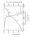
- the space 8 continues to exist at temperatures at which the thermosetting mounting agent decomposes and generates a gas. This condition will be explained, referring to the graph shown in Fig. 4.
- Fig. 4 is a graph showing how the temperature and weight of a thermosetting mounting agent vary in relation to heating time.
- curve a represents a weight-decreasing ratio of the thermosetting mounting agent
- curve b represents a temperature increase of the thermosetting mounting agent
- the weight decreasing ratio of the mounting agent is about 82.5%, as is readily understood from the graph.
- a line segment is drawn in parallel to the ordinate from that point on curve a which corresponds to time t3 until it intersects line b .
- a line segment is drawn in parallel to the abscissa until it intersects the ordinate, and the temperature value at this intersection is read.
- a weight-decreasing ration of 82.5% corresponds to a temperature of about 450°C.
- the weight of the mounting agent abruptly decreases at the point where the temperature exceeds 350°C. This means that the mounting agent is decomposed into a gas from this point. The decomposition of the mounting agent (i.e., the generation of a gas) continues until the point where the temperature is about 450°C, as may be understood from curve b in Fig. 4.
- low-melting point glass 3, 4 begins to change from a solid state into a liquid state.
- the low-melting point glass in this transition state has a certain degree of viscosity, but can keep the shape which it has in the solid state.
- the space 8 between the ceramic substrates 1 and 2 is maintained in the transition state of the low-melting point glass.
- time t3 at which the low-melting point glass changes into the liquid state should be after time t1 at which the gas generation is completed. As long as this requirement is satisfied, all gas is discharged from the semiconductor device through the space 8.
- the low-melting point glass 3, 4 changes into a liquid state, thus filling the space 8 between the two ceramic substrates 1 and 2, as is shown in Fig. 3C. More specifically, the low-melting point glass 3, 4 in the fluid state flows into the space 8. After the space 8 is filled with the low-melting point glass, the heating is stopped, so as to change the low-melting point glass back into the solid state.
- the low-melting point glass sealed semiconductor device of one embodiment of the present invention is manufactured.
- Fig. 5A is a graph showing the distribution of satisfactory and defective products, the graph being obtained by examining low-melting point glass sealed semiconductor devices whose ceramic substrates have such a shape as is determined in the present invention and by examining low-melting point glass sealed semiconductor devices whose ceramic substrates do not have such a shape as is determined in the present invention.
- the abscissa represents the maximum displacement by which the ceramic substrate 1 serving as a cap is located away from the contact plane in which substrate 1 and substrate 2 contacts each other, while the ordinate represents the maximum displacement by which the ceramic substrate 2 having a semiconductor chip thereon is located away from the same contact plane.
- the ceramic substrate illustrated in Fig. 5B has such a shape as is determined in the present invention.
- the maximum displacement of the substrate which is the distance between the contact plane to the highest point in that surface of the substrate which is coated with the low-melting point glass.
- the ceramic substrate illustrated in Fig. 5C also has a shape as is determined in the present invention, but low-melting point glass is coated on the outwardly-curved surface of this substrate. Therefore, the maximum displacement of the substrate with reference to the contact plane is represented by a positive value.
- the ceramic substrate illustrated in Fig. 5D is corrugated.
- the displacements of points located on the glass-coated surface are represented by positive values.
- Fig. 5A all satisfactory products indicated by ⁇ are in the third quadrant, where both the substrates 1 and 2 have negative displacements.
- the negative displacements of the substrates 1 and 2 are concentratedly distributed in the region from 20 ⁇ m to 120 ⁇ m.
- the upper limit of these negative displacements is determined by the size of the low-melting point glass sealed semiconductor devices, namely, the sizes of substrates 1 and 2. For example, if the substrates 1 and 2 have a surface of approximately 52 mm x 15 mm, the upper limit of the displacements is 120 ⁇ m or so.
- Defective products indicated by ⁇ and x are either in the first quadrant, where both the substrates 1 and 2 have positive displacements, or in the second and fourth quadrants, where one of the substrates has a positive displacement.
- any defective products indicated by ⁇ is a semiconductor device having two substrates of the type shown in Fig. 5C which are adhered to each other, or a substrate of type shown in Fig. 5C and another substrate of the type shown in Fig. 5B which are adhered to each other.
- the defective products indicated by x are a semiconductor device wherein at least one of the paired substrates has such a shape as is illustrated in Fig. 5D.
- Fig. 6 is a perspective view schematically showing a low-melting point glass sealed semiconductor device according to a second embodiment of the invention.
- the components identical to those shown in Fig. 3A are designated by the same numerals. Only the features which are different from those of the first embodiment will be described.
- At least those surfaces of substrates 1 and 2 which are coated with low-melting point glass layers 3 and 3, respectively, are arcuate, thus providing such a space as is provided in the first embodiment.
- both substrates 1 and 2 may be shaped like a concavo-concave lens. In this case, a space is provided between those surfaces of the substrates 1 and 3 on which low-melting point glass layers 3 and 4 are formed, respectively.
- Figs. 8A and 8C are perspective views, explaining how to manufacture a low-melting point glass sealed semiconductor device according to a fourth embodiment.
- the components identical to those shown in Figs. 3A to 3C are denoted by the same numerals.
- Figs. 8A to 8C it will be described how the semiconductor device according to the third embodiment is manufactured.
- a shallow groove is formed in that surface of ceramic substrate 2 which is used as a base and opposes ceramic substrate 1, in order to provide a space 8 between the substrates 1 and 2 as in the first embodiment.
- a semiconductor chip (not shown) is fixed onto that surface of the ceramic substrate 2 by means of thermosetting material. Then, the ceramic substrate 1, which is used as a cap, is mounted on the ceramic substrate 2, thus forming an unfinished product having the space 8 between the substrates 1 and 2.
- the unfinished product is placed in a furnace (not shown) and is heated therein, whereby the thermosetting material is thermally set, and the decomposed gas emanates from the thermosetting material.
- the unfinished product is further heated in the furnace, the low-melting point glass layers formed on the opposing surfaces of the substrates 1 and 2 melt.
- the substrate 1 is pressed onto the substrate 2 under its own weight, whereby the molten glass fills up the space 8.
- the unfinished product is cooled, and the glass solidifies.
- the semiconductor chip (not shown) is sealed in airtight fashion.
- the gas which is generated from the thermosetting mounting agent in the adhesion step hardly remains inside the device. Since the formation of voids noted above is suppressed, the semiconductor device is satisfactory in operation. Further, the method of the present invention enables such satisfactory semiconductor devices to be manufactured at high yield.
- the two ceramic substrates have substantially the same shape. Therefore, the space produced when such ceramic substrates are stacked upon each other is located in the center of the semiconductor device. Thus, the formation of voids can be effectively suppressed.
- the low-melting point glass sealed semiconductor device of the present invention is very reliable in its sealed characteristic.
- the method of the present invention enables such semiconductor devices to be manufactured at high yield, thus contributing to reduction in the manufacturing cost.
Landscapes
- Die Bonding (AREA)
Applications Claiming Priority (4)
| Application Number | Priority Date | Filing Date | Title |
|---|---|---|---|
| JP18929489 | 1989-07-21 | ||
| JP189294/89 | 1989-07-21 | ||
| JP2187753A JPH0793387B2 (ja) | 1989-07-21 | 1990-07-16 | 気密封止型半導体装置およびその製造方法 |
| JP187753/90 | 1990-07-16 |
Publications (2)
| Publication Number | Publication Date |
|---|---|
| EP0409257A2 true EP0409257A2 (fr) | 1991-01-23 |
| EP0409257A3 EP0409257A3 (en) | 1991-04-03 |
Family
ID=26504537
Family Applications (1)
| Application Number | Title | Priority Date | Filing Date |
|---|---|---|---|
| EP19900113946 Withdrawn EP0409257A3 (en) | 1989-07-21 | 1990-07-20 | Low-melting point glass sealed semiconductor device and method of manufacturing the same |
Country Status (1)
| Country | Link |
|---|---|
| EP (1) | EP0409257A3 (fr) |
Cited By (1)
| Publication number | Priority date | Publication date | Assignee | Title |
|---|---|---|---|---|
| WO1998000864A1 (fr) * | 1996-06-28 | 1998-01-08 | Siemens Aktiengesellschaft | Boitier de composant pour monter en surface un composant a semiconducteur |
Family Cites Families (3)
| Publication number | Priority date | Publication date | Assignee | Title |
|---|---|---|---|---|
| US4445274A (en) * | 1977-12-23 | 1984-05-01 | Ngk Insulators, Ltd. | Method of manufacturing a ceramic structural body |
| JPS5762539A (en) * | 1980-10-01 | 1982-04-15 | Hitachi Ltd | Mounting method for semiconductor element |
| CN87107692A (zh) * | 1986-11-13 | 1988-05-25 | Mt化学公司 | 半导体器件的制造方法 |
-
1990
- 1990-07-20 EP EP19900113946 patent/EP0409257A3/en not_active Withdrawn
Cited By (2)
| Publication number | Priority date | Publication date | Assignee | Title |
|---|---|---|---|---|
| WO1998000864A1 (fr) * | 1996-06-28 | 1998-01-08 | Siemens Aktiengesellschaft | Boitier de composant pour monter en surface un composant a semiconducteur |
| US6058020A (en) * | 1996-06-28 | 2000-05-02 | Siemens Aktiengesellschaft | Component housing for surface mounting of a semiconductor component |
Also Published As
| Publication number | Publication date |
|---|---|
| EP0409257A3 (en) | 1991-04-03 |
Similar Documents
| Publication | Publication Date | Title |
|---|---|---|
| US5888847A (en) | Technique for mounting a semiconductor die | |
| US5633528A (en) | Lead frame structure for IC devices with strengthened encapsulation adhesion | |
| EP0332402A2 (fr) | Disposition de connexion et procédé pour sa fabrication | |
| EP0860871B1 (fr) | Procédé de fabrication d'un dispositif semi-conducteur | |
| US5218229A (en) | Inset die lead frame configuration lead frame for a semiconductor device having means for improved busing and die-lead frame attachment | |
| US6204564B1 (en) | Semiconductor device and method for making the same | |
| US20050272182A1 (en) | Methods of making microelectronic packages | |
| JPH0794553A (ja) | 半導体装置およびその製造方法 | |
| US7534652B2 (en) | Microelectronic elements with compliant terminal mountings and methods for making the same | |
| TWI236740B (en) | Chip package structure | |
| US5757068A (en) | Carrier film with peripheral slits | |
| US4951120A (en) | Lead frame and semiconductor device using the same | |
| JPH0823002A (ja) | 半導体装置及びその製造方法 | |
| EP0458469A1 (fr) | Cadre conducteur composite et dispositif semi-conducteur l'utilisant | |
| JPH10270626A (ja) | 半導体装置およびその製造方法 | |
| EP0090566B1 (fr) | Empaquetage pour dispositif semi-conducteur | |
| EP0409257A2 (fr) | Dispositif semiconducteur scellé du verre à bas point de fusion et procédé de fabrication | |
| JPS62241355A (ja) | 半導体装置 | |
| JP2000114295A (ja) | 半導体装置の製造方法 | |
| EP0409004A2 (fr) | Dispositif semi-conducteur scellé du verre à bas point de fusion et son procédé de fabrication | |
| JPH07122670A (ja) | ガラス封止型半導体装置の製造方法 | |
| US5237206A (en) | Low-melting point glass sealed semiconductor device and method of manufacturing the same | |
| JPS60120543A (ja) | 半導体装置およびそれに用いるリ−ドフレ−ム | |
| JP2003017623A (ja) | 半導体装置及びその製造方法 | |
| JPH0269945A (ja) | 半導体装置及びその製造方法 |
Legal Events
| Date | Code | Title | Description |
|---|---|---|---|
| PUAI | Public reference made under article 153(3) epc to a published international application that has entered the european phase |
Free format text: ORIGINAL CODE: 0009012 |
|
| 17P | Request for examination filed |
Effective date: 19900720 |
|
| AK | Designated contracting states |
Kind code of ref document: A2 Designated state(s): DE FR GB |
|
| PUAL | Search report despatched |
Free format text: ORIGINAL CODE: 0009013 |
|
| AK | Designated contracting states |
Kind code of ref document: A3 Designated state(s): DE FR GB |
|
| STAA | Information on the status of an ep patent application or granted ep patent |
Free format text: STATUS: THE APPLICATION HAS BEEN WITHDRAWN |
|
| 18W | Application withdrawn |
Withdrawal date: 19910701 |