EP0410116B1 - Procédé de fabrication d'un dispositif semiconducteur à connexion par fil - Google Patents
Procédé de fabrication d'un dispositif semiconducteur à connexion par fil Download PDFInfo
- Publication number
- EP0410116B1 EP0410116B1 EP90110621A EP90110621A EP0410116B1 EP 0410116 B1 EP0410116 B1 EP 0410116B1 EP 90110621 A EP90110621 A EP 90110621A EP 90110621 A EP90110621 A EP 90110621A EP 0410116 B1 EP0410116 B1 EP 0410116B1
- Authority
- EP
- European Patent Office
- Prior art keywords
- shock
- frame
- semiconductor chip
- absorbing layer
- semiconductor device
- Prior art date
- Legal status (The legal status is an assumption and is not a legal conclusion. Google has not performed a legal analysis and makes no representation as to the accuracy of the status listed.)
- Expired - Lifetime
Links
Images

Classifications
-
- H—ELECTRICITY
- H10—SEMICONDUCTOR DEVICES; ELECTRIC SOLID-STATE DEVICES NOT OTHERWISE PROVIDED FOR
- H10W—GENERIC PACKAGES, INTERCONNECTIONS, CONNECTORS OR OTHER CONSTRUCTIONAL DETAILS OF DEVICES COVERED BY CLASS H10
- H10W70/00—Package substrates; Interposers; Redistribution layers [RDL]
- H10W70/40—Leadframes
- H10W70/421—Shapes or dispositions
- H10W70/442—Shapes or dispositions of multiple leadframes in a single chip
-
- H—ELECTRICITY
- H10—SEMICONDUCTOR DEVICES; ELECTRIC SOLID-STATE DEVICES NOT OTHERWISE PROVIDED FOR
- H10W—GENERIC PACKAGES, INTERCONNECTIONS, CONNECTORS OR OTHER CONSTRUCTIONAL DETAILS OF DEVICES COVERED BY CLASS H10
- H10W70/00—Package substrates; Interposers; Redistribution layers [RDL]
- H10W70/40—Leadframes
- H10W70/411—Chip-supporting parts, e.g. die pads
- H10W70/415—Leadframe inner leads serving as die pads
-
- H—ELECTRICITY
- H10—SEMICONDUCTOR DEVICES; ELECTRIC SOLID-STATE DEVICES NOT OTHERWISE PROVIDED FOR
- H10W—GENERIC PACKAGES, INTERCONNECTIONS, CONNECTORS OR OTHER CONSTRUCTIONAL DETAILS OF DEVICES COVERED BY CLASS H10
- H10W70/00—Package substrates; Interposers; Redistribution layers [RDL]
- H10W70/40—Leadframes
- H10W70/456—Materials
- H10W70/458—Materials of insulating layers on leadframes
-
- H—ELECTRICITY
- H10—SEMICONDUCTOR DEVICES; ELECTRIC SOLID-STATE DEVICES NOT OTHERWISE PROVIDED FOR
- H10W—GENERIC PACKAGES, INTERCONNECTIONS, CONNECTORS OR OTHER CONSTRUCTIONAL DETAILS OF DEVICES COVERED BY CLASS H10
- H10W72/00—Interconnections or connectors in packages
- H10W72/50—Bond wires
-
- H—ELECTRICITY
- H10—SEMICONDUCTOR DEVICES; ELECTRIC SOLID-STATE DEVICES NOT OTHERWISE PROVIDED FOR
- H10W—GENERIC PACKAGES, INTERCONNECTIONS, CONNECTORS OR OTHER CONSTRUCTIONAL DETAILS OF DEVICES COVERED BY CLASS H10
- H10W74/00—Encapsulations, e.g. protective coatings
-
- H—ELECTRICITY
- H10—SEMICONDUCTOR DEVICES; ELECTRIC SOLID-STATE DEVICES NOT OTHERWISE PROVIDED FOR
- H10W—GENERIC PACKAGES, INTERCONNECTIONS, CONNECTORS OR OTHER CONSTRUCTIONAL DETAILS OF DEVICES COVERED BY CLASS H10
- H10W90/00—Package configurations
- H10W90/701—Package configurations characterised by the relative positions of pads or connectors relative to package parts
- H10W90/751—Package configurations characterised by the relative positions of pads or connectors relative to package parts of bond wires
- H10W90/756—Package configurations characterised by the relative positions of pads or connectors relative to package parts of bond wires between a chip and a stacked lead frame, conducting package substrate or heat sink
Definitions
- the present invention relates to a semiconductor device, wherein a semiconductor chip is mounted on the bed of a first frame, the tip end of each of the inner leads of a second frame is located above the semiconductor chip, and the bonding pads of the semiconductor chip and the inner leads of the second frame are connected together by bonding wires.
- the present invention also relates to a method for manufacturing this type of semiconductor device.
- the above-mentioned type of semiconductor device is advantageous, in that a comparatively small-sized package, formed of sealing resin, can be employed for housing a large-sized chip.
- EP-A-0 108 502 and EP-A-0 354 696 show insulating layers which can protect the semiconductor layers from damage by bonding wires or inner leads.
- the inventor of the present invention considered coating the surface of the semiconductor chip with a shock-absorbing film.
- the thickness of the film has to be more than a certain value. If the coated film is too thick, it contracts during the coating step. Since, in this case, the wafer coated with the film is subjected to physical stress, it may warp, resulting in damage to it.
- the inventor also considered forming a shock-absorbing film on those portions of the second frame which face the semiconductor chip, so as to sufficiently absorb a shock.
- the interface between different materials is likely to become a water route along which water enters the interior of a resin-sealed semiconductor device. Therefore, if the shock-absorbing film is formed on the second frame, not only the interface between the molded resin and the second frame but also the interface between the molded resin and the shock-absorbing film may become a water route. Thus, water is easy to enter the interior of a semiconductor device if this semiconductor device has a shock-absorbing film coated on the second frame.
- an object of the present invention is to prevent application of shock, when bonding is performed on a semiconductor chip to fabricate a semiconductor device.
- Another object of the invention is to improve both the reliability and manufacturing yield of semiconductor devices to be fabricated.
- the present invention provides a method of manufacturing a semiconductor device, comprising the steps: applying a layer of shock-absorbing electrically insulating material to a predetermined portion on one side of a plate-like second lead frame material; punching the second lead frame material, applied with the shock-absorbing layer material, into a predetermined shape, to thereby form a second lead frame having a plurality of inner leads and a shock-absorbing layer applied at least to the tip end of each inner lead; preparing a first lead frame having a chip-support bed; mounting a semiconductor chip having a plurality of bonding pads on the surface opposing the mounting surface thereof on said bed; adjusting the position of the second lead frame such that the inner leads of the second lead frame are located above said opposing surface of the semiconductor chip and such that the shock-absorbing layer faces said opposing surface of the semiconductor chip; and connecting respective ones of the bonding pads of the semiconductor chip to respective ones of the tip ends of the inner leads by bonding wires.
- the shock-absorbing layer is formed on that surface portion of the inner lead which faces the semiconductor chip. Since the shock-absorbing layer serves to absorb a shock which may be applied to the semiconductor chip during a bonding operation, the semiconductor chip is prevented from cracking and the semiconductor element is prevented from being damaged. It should be also noted that the shock-absorbing layer is formed only at a portion where it is necessary, and that the shock-absorbing layer is not exposed to the outside after the semiconductor chip is sealed by a sealing resin layer. Since, therefore, the interface between the shock-absorbing layer and a member in contact therewith does not become a water route, electric leakage arising from the provision of the shock-absorbing layer is prevented.
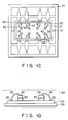
- Figs. 1A through 1D are views illustrating the steps of an example of a process by which to manufacture a semiconductor device of the present invention.
- a plate-like second frame material 36 is prepared.
- This material 36 is a Fe-Ni alloy such as 42-alloy, Cu, or the like.
- a sheet-like shock-absorbing layer material 52 is applied to a predetermined portion on one side of the plate-like second frame material 36. Any kind of material may be used as the shock-absorbing layer material 52, as long as it is an electric insulator and can resist such heat as is produced in the heating atmosphere utilized in the manufacturing process of the semiconductor device.
- the shock-absorbing layer material 52 epoxy resin may be used, but polyimide resin is more desirable.
- the thickness of the shock-absorbing layer material 52 is preferably within the range of 30 to 50 ⁇ m.
- the application of the shock-absorbing layer material to the second frame material is carried out, for example, by the adhesion used in a printing process.
- the second frame material 36 applied with the shock-absorbing layer material 52, is punched into a predetermined shape, to thereby form a second frame 30 (which is indicated by the oblique lines in the Figures).
- the second frame 30 has inner leads 32 and shock-absorbing layers 50 adhered at least to the tip end 34 of each inner lead 32.
- the second frame material 36 is punched from the side to which the shock-absorbing layer material 52 is applied, since the punching from this side leaves no burr.
- a first frame 10 having a bed 12 is prepared, as is shown in Fig. 1C.
- a semiconductor chip 20 having bonding pads 22 is mounted on the bed 12.
- the position of the second frame 30 is adjusted such that the inner leads 32 of the second frame 30 are located above the semiconductor chip 20 and such that the shock-absorbing layers 50 face the surface of the semiconductor chip 20.
- the first frame 10 and the second frame 30 are bonded together by spot welding.
- the bonding pads 22 of the semiconductor chip 20 are connected, by means of bonding wires 40, to the tip ends 34 of the corresponding inner leads 32 of the second frame 30 which is located above the semiconductor chip 20.
- a sealing resin layer 60 is provided for the region indicated by the two-dot-dash lines in the Figures.
- a semiconductor device manufactured in the above-mentioned manner comprises: a first frame 10 having a bed 12; a semiconductor chip 20 mounted on the bed 12 and having a bonding pad 22; a second frame 30 having an inner lead located above the semiconductor chip 20; a bonding wire 40 connecting the bonding pad 22 of the semiconductor chip 20 to the tip end 34 of the inner lead 32; and a shock-absorbing layer 50 which is adhered at least to that surface portion of the tip end 34 of the inner lead 32 which faces the semiconductor chip 20.
Landscapes
- Wire Bonding (AREA)
- Lead Frames For Integrated Circuits (AREA)
- Structures Or Materials For Encapsulating Or Coating Semiconductor Devices Or Solid State Devices (AREA)
Claims (5)
- Procédé de fabrication d'un dispositif à semiconducteur, comprenant les étapes consistant à:- appliquer une couche de matière électriquement isolante absorbant les chocs (52) à une partie prédéterminée sur un côté d'une matière d'un deuxième cadre à conducteurs en forme de plaque 36;- découper au poinçon la matière du deuxième cadre à conducteurs (36) ayant la matière absorbant les chocs (52) pour lui donner une forme prédéterminée pour former par ce moyen un deuxième cadre à conducteurs (30) ayant une pluralité de conducteurs intérieurs et une couche absorbant les chocs (50) appliquée à au moins l'extrémité (34) de chaque conducteur intérieur (32);- confectionner un premier cadre à conducteurs 10 ayant une surface de portée (12) pour supporter une puce; monter une puce de semiconducteur (20) ayant une pluralité de plages de connexion (22) sur la surface opposée à la surface de montage de celle-ci sur la surface de portée (12);- régler la position du deuxième cadre à conducteurs (30) de telle manière que les conducteurs intérieurs (32) du deuxième cadre à conducteurs (30) soient situés au-dessus de ladite surface opposée de la puce de semiconducteur (32) et de telle manière que la couche absorbant les chocs fasse face à ladite surface opposée de la puce de semiconducteur (20); et- connecter les plages de connexion respectives de la puce de semiconducteur (20) aux extrémités respectives (34) des conducteurs intérieurs (32) par des fils de connexion soudés (4).
- Procédé selon la revendication 1, caractérisé en ce que ladite étape d'application comprend une étape consistant à coller la matière du deuxième cadre à conducteurs (52) à la matière du deuxième cadre à conducteurs (36) à l'aide d'un adhésif.
- Procédé selon la revendication 1, caractérisé en ce que ladite étape d'application comprend une étape consistant à coller la matière absorbant les chocs (52) à la matière du deuxième cadre (36) par sérigraphie.
- Procédé selon la revendication 1, 2 ou 3, caractérisé en ce qu'il comprend en outre une étape consistant à enrober hermétiquement avec de la résine le premier cadre à conducteurs (10), la puce de semiconducteur (20), le deuxième cadre (30), les fils de connexion soudés (40) et la couche absorbant les chocs (50).
- Procédé selon l'une quelconque des revendications précédentes, caractérisé en ce que ladite étape de découpage au poinçon comprend une étape consistant à découper au poinçon la matière du deuxième cadre (36) à partir du côté auquel la matière absorbant les chocs (52) est appliquée.
Applications Claiming Priority (2)
| Application Number | Priority Date | Filing Date | Title |
|---|---|---|---|
| JP1163686A JPH0650749B2 (ja) | 1989-06-28 | 1989-06-28 | 半導体装置及びその製造方法 |
| JP163686/89 | 1989-06-28 |
Publications (3)
| Publication Number | Publication Date |
|---|---|
| EP0410116A2 EP0410116A2 (fr) | 1991-01-30 |
| EP0410116A3 EP0410116A3 (en) | 1992-05-06 |
| EP0410116B1 true EP0410116B1 (fr) | 1995-09-06 |
Family
ID=15778670
Family Applications (1)
| Application Number | Title | Priority Date | Filing Date |
|---|---|---|---|
| EP90110621A Expired - Lifetime EP0410116B1 (fr) | 1989-06-28 | 1990-06-05 | Procédé de fabrication d'un dispositif semiconducteur à connexion par fil |
Country Status (4)
| Country | Link |
|---|---|
| EP (1) | EP0410116B1 (fr) |
| JP (1) | JPH0650749B2 (fr) |
| KR (1) | KR930009014B1 (fr) |
| DE (1) | DE69022146T2 (fr) |
Families Citing this family (2)
| Publication number | Priority date | Publication date | Assignee | Title |
|---|---|---|---|---|
| JPH0693469B2 (ja) * | 1989-11-28 | 1994-11-16 | 株式会社東芝 | 樹脂封止型半導体装置 |
| US9859680B2 (en) | 2013-12-17 | 2018-01-02 | Lasermax, Inc. | Shock resistant laser module |
Family Cites Families (2)
| Publication number | Priority date | Publication date | Assignee | Title |
|---|---|---|---|---|
| JPS5966157A (ja) * | 1982-10-08 | 1984-04-14 | Fujitsu Ltd | 半導体装置及びその製造方法 |
| JP2522524B2 (ja) * | 1988-08-06 | 1996-08-07 | 株式会社東芝 | 半導体装置の製造方法 |
-
1989
- 1989-06-28 JP JP1163686A patent/JPH0650749B2/ja not_active Expired - Fee Related
-
1990
- 1990-06-05 EP EP90110621A patent/EP0410116B1/fr not_active Expired - Lifetime
- 1990-06-05 DE DE69022146T patent/DE69022146T2/de not_active Expired - Fee Related
- 1990-06-28 KR KR1019900009628A patent/KR930009014B1/ko not_active Expired - Fee Related
Also Published As
| Publication number | Publication date |
|---|---|
| DE69022146T2 (de) | 1996-03-21 |
| JPH0330344A (ja) | 1991-02-08 |
| KR930009014B1 (ko) | 1993-09-18 |
| EP0410116A3 (en) | 1992-05-06 |
| JPH0650749B2 (ja) | 1994-06-29 |
| KR910001958A (ko) | 1991-01-31 |
| DE69022146D1 (de) | 1995-10-12 |
| EP0410116A2 (fr) | 1991-01-30 |
Similar Documents
| Publication | Publication Date | Title |
|---|---|---|
| US5539251A (en) | Tie bar over chip lead frame design | |
| US5793108A (en) | Semiconductor integrated circuit having a plurality of semiconductor chips | |
| US5567656A (en) | Process for packaging semiconductor device | |
| US6204564B1 (en) | Semiconductor device and method for making the same | |
| KR100199262B1 (ko) | 반도체장치 및 그 제조방법 | |
| JP2005519471A (ja) | 積層ダイ半導体装置 | |
| US7557454B2 (en) | Assemblies with bond pads of two or more semiconductor devices electrically connected to the same surface of a plurality of leads | |
| JPH08293524A (ja) | 半導体装置およびその製造方法 | |
| US6277670B1 (en) | Semiconductor chip package and fabrication method thereof | |
| US5757068A (en) | Carrier film with peripheral slits | |
| US5296737A (en) | Semiconductor device with a plurality of face to face chips | |
| US5278101A (en) | Semiconductor device and method for manufacturing the same | |
| US5780923A (en) | Modified bus bar with Kapton™ tape or insulative material on LOC packaged part | |
| KR100391094B1 (ko) | 듀얼 다이 패키지와 그 제조 방법 | |
| EP0631315A1 (fr) | Boîtier pour circuit intégré semi-conducteur du type "Lead on chip" (LOC) | |
| EP0410116B1 (fr) | Procédé de fabrication d'un dispositif semiconducteur à connexion par fil | |
| US6133624A (en) | Semiconductor device utilizing a lead on chip structure | |
| US5532189A (en) | Method of making semiconductor package | |
| JP3555790B2 (ja) | 半導体装置 | |
| JPH09172126A (ja) | 樹脂封止型半導体装置およびその製造方法 | |
| KR950003904B1 (ko) | 반도체 패키지 | |
| KR100214857B1 (ko) | 멀티 칩 패키지 | |
| JP3145892B2 (ja) | 樹脂封止型半導体装置 | |
| JP2972679B2 (ja) | リードフレーム並びに樹脂封止型半導体装置及びその製造方法 | |
| JPH06334106A (ja) | 樹脂封止型半導体装置 |
Legal Events
| Date | Code | Title | Description |
|---|---|---|---|
| PUAI | Public reference made under article 153(3) epc to a published international application that has entered the european phase |
Free format text: ORIGINAL CODE: 0009012 |
|
| 17P | Request for examination filed |
Effective date: 19900605 |
|
| AK | Designated contracting states |
Kind code of ref document: A2 Designated state(s): DE FR GB |
|
| PUAL | Search report despatched |
Free format text: ORIGINAL CODE: 0009013 |
|
| AK | Designated contracting states |
Kind code of ref document: A3 Designated state(s): DE FR GB |
|
| 17Q | First examination report despatched |
Effective date: 19940719 |
|
| GRAA | (expected) grant |
Free format text: ORIGINAL CODE: 0009210 |
|
| AK | Designated contracting states |
Kind code of ref document: B1 Designated state(s): DE FR GB |
|
| REF | Corresponds to: |
Ref document number: 69022146 Country of ref document: DE Date of ref document: 19951012 |
|
| ET | Fr: translation filed | ||
| PLBE | No opposition filed within time limit |
Free format text: ORIGINAL CODE: 0009261 |
|
| STAA | Information on the status of an ep patent application or granted ep patent |
Free format text: STATUS: NO OPPOSITION FILED WITHIN TIME LIMIT |
|
| 26N | No opposition filed | ||
| PGFP | Annual fee paid to national office [announced via postgrant information from national office to epo] |
Ref country code: GB Payment date: 19970527 Year of fee payment: 8 |
|
| PGFP | Annual fee paid to national office [announced via postgrant information from national office to epo] |
Ref country code: FR Payment date: 19970610 Year of fee payment: 8 |
|
| PG25 | Lapsed in a contracting state [announced via postgrant information from national office to epo] |
Ref country code: GB Free format text: LAPSE BECAUSE OF NON-PAYMENT OF DUE FEES Effective date: 19980605 |
|
| GBPC | Gb: european patent ceased through non-payment of renewal fee |
Effective date: 19980605 |
|
| PG25 | Lapsed in a contracting state [announced via postgrant information from national office to epo] |
Ref country code: FR Free format text: LAPSE BECAUSE OF NON-PAYMENT OF DUE FEES Effective date: 19990226 |
|
| REG | Reference to a national code |
Ref country code: FR Ref legal event code: ST |
|
| PGFP | Annual fee paid to national office [announced via postgrant information from national office to epo] |
Ref country code: DE Payment date: 20060601 Year of fee payment: 17 |
|
| PG25 | Lapsed in a contracting state [announced via postgrant information from national office to epo] |
Ref country code: DE Free format text: LAPSE BECAUSE OF NON-PAYMENT OF DUE FEES Effective date: 20080101 |