EP0412893B1 - Verfahren zum Herstellen von Kartenkörpern und Karten mit graphischen Elementen und so erhaltene Karten - Google Patents
Verfahren zum Herstellen von Kartenkörpern und Karten mit graphischen Elementen und so erhaltene Karten Download PDFInfo
- Publication number
- EP0412893B1 EP0412893B1 EP90402246A EP90402246A EP0412893B1 EP 0412893 B1 EP0412893 B1 EP 0412893B1 EP 90402246 A EP90402246 A EP 90402246A EP 90402246 A EP90402246 A EP 90402246A EP 0412893 B1 EP0412893 B1 EP 0412893B1
- Authority
- EP
- European Patent Office
- Prior art keywords
- support element
- principal
- mould
- faces
- imprint
- Prior art date
- Legal status (The legal status is an assumption and is not a legal conclusion. Google has not performed a legal analysis and makes no representation as to the accuracy of the status listed.)
- Expired - Lifetime
Links
Images


Classifications
-
- G—PHYSICS
- G06—COMPUTING OR CALCULATING; COUNTING
- G06K—GRAPHICAL DATA READING; PRESENTATION OF DATA; RECORD CARRIERS; HANDLING RECORD CARRIERS
- G06K19/00—Record carriers for use with machines and with at least a part designed to carry digital markings
- G06K19/06—Record carriers for use with machines and with at least a part designed to carry digital markings characterised by the kind of the digital marking, e.g. shape, nature, code
- G06K19/067—Record carriers with conductive marks, printed circuits or semiconductor circuit elements, e.g. credit or identity cards also with resonating or responding marks without active components
- G06K19/07—Record carriers with conductive marks, printed circuits or semiconductor circuit elements, e.g. credit or identity cards also with resonating or responding marks without active components with integrated circuit chips
- G06K19/077—Constructional details, e.g. mounting of circuits in the carrier
- G06K19/0772—Physical layout of the record carrier
- G06K19/07724—Physical layout of the record carrier the record carrier being at least partially made by a molding process
-
- B—PERFORMING OPERATIONS; TRANSPORTING
- B29—WORKING OF PLASTICS; WORKING OF SUBSTANCES IN A PLASTIC STATE IN GENERAL
- B29C—SHAPING OR JOINING OF PLASTICS; SHAPING OF MATERIAL IN A PLASTIC STATE, NOT OTHERWISE PROVIDED FOR; AFTER-TREATMENT OF THE SHAPED PRODUCTS, e.g. REPAIRING
- B29C45/00—Injection moulding, i.e. forcing the required volume of moulding material through a nozzle into a closed mould; Apparatus therefor
- B29C45/14—Injection moulding, i.e. forcing the required volume of moulding material through a nozzle into a closed mould; Apparatus therefor incorporating preformed parts or layers, e.g. injection moulding around inserts or for coating articles
- B29C45/14639—Injection moulding, i.e. forcing the required volume of moulding material through a nozzle into a closed mould; Apparatus therefor incorporating preformed parts or layers, e.g. injection moulding around inserts or for coating articles for obtaining an insulating effect, e.g. for electrical components
- B29C45/14647—Making flat card-like articles with an incorporated IC or chip module, e.g. IC or chip cards
-
- B—PERFORMING OPERATIONS; TRANSPORTING
- B29—WORKING OF PLASTICS; WORKING OF SUBSTANCES IN A PLASTIC STATE IN GENERAL
- B29C—SHAPING OR JOINING OF PLASTICS; SHAPING OF MATERIAL IN A PLASTIC STATE, NOT OTHERWISE PROVIDED FOR; AFTER-TREATMENT OF THE SHAPED PRODUCTS, e.g. REPAIRING
- B29C45/00—Injection moulding, i.e. forcing the required volume of moulding material through a nozzle into a closed mould; Apparatus therefor
- B29C45/14—Injection moulding, i.e. forcing the required volume of moulding material through a nozzle into a closed mould; Apparatus therefor incorporating preformed parts or layers, e.g. injection moulding around inserts or for coating articles
- B29C45/14688—Coating articles provided with a decoration
-
- G—PHYSICS
- G06—COMPUTING OR CALCULATING; COUNTING
- G06K—GRAPHICAL DATA READING; PRESENTATION OF DATA; RECORD CARRIERS; HANDLING RECORD CARRIERS
- G06K19/00—Record carriers for use with machines and with at least a part designed to carry digital markings
- G06K19/06—Record carriers for use with machines and with at least a part designed to carry digital markings characterised by the kind of the digital marking, e.g. shape, nature, code
- G06K19/067—Record carriers with conductive marks, printed circuits or semiconductor circuit elements, e.g. credit or identity cards also with resonating or responding marks without active components
- G06K19/07—Record carriers with conductive marks, printed circuits or semiconductor circuit elements, e.g. credit or identity cards also with resonating or responding marks without active components with integrated circuit chips
- G06K19/077—Constructional details, e.g. mounting of circuits in the carrier
-
- B—PERFORMING OPERATIONS; TRANSPORTING
- B29—WORKING OF PLASTICS; WORKING OF SUBSTANCES IN A PLASTIC STATE IN GENERAL
- B29C—SHAPING OR JOINING OF PLASTICS; SHAPING OF MATERIAL IN A PLASTIC STATE, NOT OTHERWISE PROVIDED FOR; AFTER-TREATMENT OF THE SHAPED PRODUCTS, e.g. REPAIRING
- B29C45/00—Injection moulding, i.e. forcing the required volume of moulding material through a nozzle into a closed mould; Apparatus therefor
- B29C45/14—Injection moulding, i.e. forcing the required volume of moulding material through a nozzle into a closed mould; Apparatus therefor incorporating preformed parts or layers, e.g. injection moulding around inserts or for coating articles
- B29C45/14065—Positioning or centering articles in the mould
- B29C2045/14106—Positioning or centering articles in the mould using electrostatic attraction or static electricity
-
- B—PERFORMING OPERATIONS; TRANSPORTING
- B29—WORKING OF PLASTICS; WORKING OF SUBSTANCES IN A PLASTIC STATE IN GENERAL
- B29C—SHAPING OR JOINING OF PLASTICS; SHAPING OF MATERIAL IN A PLASTIC STATE, NOT OTHERWISE PROVIDED FOR; AFTER-TREATMENT OF THE SHAPED PRODUCTS, e.g. REPAIRING
- B29C45/00—Injection moulding, i.e. forcing the required volume of moulding material through a nozzle into a closed mould; Apparatus therefor
- B29C45/14—Injection moulding, i.e. forcing the required volume of moulding material through a nozzle into a closed mould; Apparatus therefor incorporating preformed parts or layers, e.g. injection moulding around inserts or for coating articles
- B29C2045/1486—Details, accessories and auxiliary operations
- B29C2045/14967—Injecting through an opening of the insert
- B29C2045/14975—Injecting through an opening of the insert the injection nozzle penetrating through the insert
-
- B—PERFORMING OPERATIONS; TRANSPORTING
- B29—WORKING OF PLASTICS; WORKING OF SUBSTANCES IN A PLASTIC STATE IN GENERAL
- B29C—SHAPING OR JOINING OF PLASTICS; SHAPING OF MATERIAL IN A PLASTIC STATE, NOT OTHERWISE PROVIDED FOR; AFTER-TREATMENT OF THE SHAPED PRODUCTS, e.g. REPAIRING
- B29C45/00—Injection moulding, i.e. forcing the required volume of moulding material through a nozzle into a closed mould; Apparatus therefor
- B29C45/14—Injection moulding, i.e. forcing the required volume of moulding material through a nozzle into a closed mould; Apparatus therefor incorporating preformed parts or layers, e.g. injection moulding around inserts or for coating articles
- B29C45/14065—Positioning or centering articles in the mould
Definitions
- the subject of the present invention is the production of card bodies, in particular with electronic memory, which include a graphic on at least one of their main faces, this graphic being able to consist of alphanumeric information or of drawings for decorative or advertising purposes.
- the part on which it is necessary to carry out the printing has relatively reduced dimensions.
- the flexural properties of the part to be printed are very different from those of the supports. usual printing.
- the fact of making a single "image” or a limited number of images on each pass is expensive and requires precise positioning of the part each time with respect to the printing machine.
- the bonding of a preprinted sheet on parts of reduced dimensions is practically excluded for reasons of prohibitive costs.
- an object of the invention is to provide a method for producing card bodies which makes it possible to produce very good quality graphics under acceptable economic conditions while being compatible with the use of a technique. by injection molding.
- the realization of the graphics is done during the molding step itself.
- the print media are cut from preprinted sheets which have a large number of identical patterns. Their cost is therefore reduced since it uses perfectly conventional printing techniques.
- the printing supports being placed in the mold cavity, the graphics are automatically "positioned" relative to the body of the card.
- the invention also relates to the application of said card body production method to the manufacture of a complete card, that is to say of a card further comprising an electronic module fixed to the card body.
- Figure 1 shows a top view of an electronic memory card of known type.
- the card 12 comprises a card body 14 of rectangular parallelepiped shape of length L, width 1 and thickness e.
- L is 85mm
- l is 55mm
- e is 0.8mm.
- the body 14 must satisfy a certain number of tests, in particular as regards its flexural properties. It is made of a plastic material.
- electrical contact pads 18 There are eight for example. The shape and dimensions of these contacts, as well as their position relative to the edges of the card body are also the subject of ISO standard 7810.
- the front face 16 of the card body always has a graphic 20 represented by hatching on the figure.
- graphic design is meant either decorative or advertising designs or alphanumeric mentions or a combination of the two.
- the rear face 22 of the card body also includes a graphic.
- the card also includes an electronic module, not visible in the figure, including in particular an integrated circuit, the terminals of which are connected to the contact pads 18.
- the invention relates to a method for producing a card body by injection molding of a thermoplastic material which directly includes a graphic on at least one of its main faces, typically the front face 16.
- a thermoplastic material which directly includes a graphic on at least one of its main faces, typically the front face 16.
- an individual card body is molded directly with its graphics.
- mold a plate with a plurality of graphics and then cut this plate to obtain the card bodies.
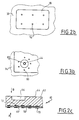
- An injection mold 30 which comprises a fixed part 32 and a movable part 34.
- the parts 32 and 34 define an imprint 36 which has the shape which it is desired to give to the card body.
- the main wall 38 of the part 32 defines a main face of the card body while the main wall 40 of the part 34 defines the other main face.
- the distance between the two main faces 38 and 40 is therefore equal to e and each main wall has the shape of a rectangle whose dimensions are equal to l and L.
- the card body in the case of an electronic memory card, must have a cavity to allow the installation of the electronic module.
- the part 34 of the mold comprises a core 42 which projects into the cavity 36.
- the core has, in negative, the shape which one wishes to give to the cavity.
- the French patent already cited gives possible forms of the nucleus.
- the core 42 is pierced by an injection nozzle 44 allowing the molding material to penetrate inside the cavity 36.
- a graphics support element or label is first produced from a support strip on which a very large number of identical graphics are produced. By cutting, a label is separated from the rest of the strip.
- the support strip can be made of an opaque material which lends itself well to printing by screen printing or by offset.
- a polyester film having a thickness of 50 to 80 microns can be used. You can also use polystyrenes regenerated or not.
- the film has a different graphic on each of its faces. After cutting each label therefore has a different graphic on each of its faces.
- the label is cut to have exactly the same dimensions as the main faces of the card body.
- the mold 30 being open, the label 50 is put in place so that it is applied against the main wall 38 of the movable part 32 of the mold.
- the part 32 of the mold has a number of orifices 52 of very small diameter (for example 0.2 mm) which open into the main wall 38.
- the orifices 52 are connected to a vacuum system.
- the mold is closed and the molding material is injected into the cavity 36 through the nozzle 44.
- the thermoplastic material injected is transparent ABS in the example described here, the injection conditions are those which have been described in the French patent already cited.
- the molding material fills the entire imprint and, taking into account its temperature and its relative fluidity, it adheres to the face 50a of the label 50. If the material of which the label 50 is made is not compatible with the molding material, an adhesive varnish can be deposited on the graphics of the face 50a of the label.
- Figure 2c shows in cross section the card body 60 obtained by the technique which has just been described.
- the card body itself 62 is transparent.
- In its main face 64 opens the cavity 66 used to house the electronic module.
- On its second main face 68 is fixed the label 50. If we look at the card body according to the arrow A we can directly see the graphic 70 produced on the external face of the label 50. If we look at the body card according to arrow B we see the graphic 72 produced on the internal face of the label 50 through the body 62 which is transparent.
- Figures 3a and 3b illustrate a second example of the first embodiment of the invention. It is particularly well suited to the case where the cavity to be produced in the card body is deep compared to the thickness of the card body.
- the mold 30 ′ is identical to the mold 30 in FIG. 2 a with two differences.
- the suction orifices 80 open into the main face 40 of the fixed part 34 of the mold.
- the core 82 which always includes the injection nozzle 44 has a different shape to produce a deeper cavity. In other words, the end 82 a of the core 82 is closer to the main wall 38.
- suction holes 80 are arranged in a ring in close proximity to the core 82.
- a label 84 is used which is identical to the label 50 of FIG. 2a, except for the presence of a window 88.
- the label 84 is placed in the mold against the main wall 40 so that the core 82 passes through the window 88.
- a clearance must be left, for example 1 / 10th of a mm, between the periphery of the core 82 and the edge of the window 88.
- the plastic material is injected into the cavity 36 as has already been described in connection with FIGS. 2a and 2b. Then we unmold the card body thus produced. This is for example ABS.
- suction holes 80 arranged around the core 82 allow the part of the label which surrounds the window 88 to be pressed against the wall 40 and therefore prevent this part of the label from moving away of the wall 40 under the effect of the circulation of the molding material during the injection.
- the distance a between the end 82 a of the core and the wall 38 remains sufficient to allow injection under normal conditions.
- FIG. 3c illustrates a fourth example of the first embodiment of the invention.
- the mold 30 '' differs from the mold 30 'essentially in that the core 82' only serves to define the cavity to be produced in the card body and the injection nozzle 44 'opens into the side wall 39 of part 32 of the mold.
- suction holes 52 ′ open into the main wall 38 of the part 32 of the mold to hold the label 84 pressed against this wall.
- FIG. 4 illustrates a third example of the first embodiment of the invention.
- the graphics on the two main faces of the card body are produced using two labels 90 and 92.
- the label 90 carries a graphic only on its face 94.
- the label 92 carries a graphic only on its face 96 and includes a window 98.
- the mold 30 '' includes a fixed portion 32 identical to that of the mold 30 of Figure 2a and a movable part 34 identical to that of the mold 30 'in Figure 3a.
- the labels 90 and 92 are placed in the mold as shown in FIG. 4.
- the mold 30 ' is closed and the injection is carried out. In this case it is of course not necessary to use a transparent molding material. Then we unmold card body.
- the labels are cut from a pre-printed polyester film with a thickness of 50 to 80 microns. It goes without saying that other material could be used, for example paper of suitable quality and of sufficiently reduced thickness so as not to occupy too much space in the mold.
- each card body was molded individually. It should be understood by this that at the exit of the mold the card body already has its exterior shape. However, it is very clear that the same injection machine can comprise several imprints linked together by a set of injection channels supplying the injection nozzles.
- the label or labels are held against the main wall of the mold using suction holes. Keeping labels in place can also be achieved in the following manner: We exploit the fact that the strip on which the graphics are produced and therefore the labels which are cut from this strip are generally electrically charged due to the nature of the material. and manipulations performed on this tape. If the mold is kept grounded, the electrically charged label is pressed against the main wall of the mold and is held there. To ensure that the label has sufficient electrical charge, it is preferable to pass the strip used to make the labels in a polarizing device.
- the plate After removing the plate from the mold, the plate is cut to individualize each card body.
- the bodies of card can be of one of the three types already described, namely: transparent body and label on the front face, transparent body and label on the rear face, and non-transparent body and label on each of the faces.
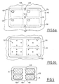
- FIG. 5 shows a support element 102 which can be used for the second embodiment of the invention. It consists of a portion of a non-transparent film identical to that which has been described in connection with FIGS. 2 to 4.
- Each graphic A has the dimensions L and l of a main face of the card body.
- Each graphic A is surrounded by an unprinted area 108.
- FIGS. 6a and 6b show the form of a mold usable for the second embodiment of the invention, FIG. 6a showing the fixed part 110 of the mold and FIG. 6b its movable part 112.
- the fixed part has an imprint 114 which defines a main wall 116 and a side wall 118.
- the main wall 116 protrude four cores 120 intended to produce the cavities of the four card bodies.
- Injection nozzles 122 to 126 open into the wall 116.
- the outline of the card bodies to be produced has been shown in dotted lines 128.
- the injection nozzles 122 to 126 open into the wall 116 outside the zones 128 corresponding to the card bodies.
- the height of the cores 120 is not too great, it is advantageous to unblock the injection nozzles in the cores 120 as has been described in detail in connection with FIGS. 2 to 4.
- the movable part 112 of the mold defines the second main wall 130 of the mold.
- These orifices 132 have the same dimensions as the orifices 52 in FIG. 2a and they are more particularly concentrated in the areas 128 corresponding to the different card bodies.
- the support element 102 is placed against the wall 130 of the movable part of the mold, and the suction system is started. Then the mold is closed and the plastic material is injected, which is for example transparent ABS. When the plastic material is solidified, the mold is opened. One then obtains a plate of thickness e comprising four cavities and provided on one of its faces with graphic patterns.
- the plate thus obtained is cut to produce four card bodies which are identical to that which is shown in FIG. 2c.
- the support element includes positioning marks to allow precise cutting of the card body.
- a complete card includes not only a card body but also an electronic module mounted in the cavity of the card body.
- the electronic module essentially comprises a semiconductor patch in which electronic circuits are produced, external electrical contact pads, visible at 18 in FIG. 1, electrical connections between the contact pads and the terminals of the semiconductor patch and, most often, a coating material to protect the semiconductor wafer and the electrical connections.
- Electronic modules for smart cards can have different forms and organizations. In particular, the external electrical contact pads as well as the electrical connections can be made in different ways.
- the US patents 4,625,102 and 4,737,620 describe several embodiments of these modules.
- a mold 31 is used which is identical to the mold 30 '' in FIG. 3c with the following difference:
- the core 82 is removed and it is replaced by suction orifices such as 150.
- the portion of the wall 40 of the part 34 of the mold where the core 82 'protrudes is provided with small positioning lugs 152.
- FIG. 8 shows a second embodiment of a complete map.
- the mold 31 ′ used is identical to the mold 31 in FIG. 7. However, as shown in FIG. 8, it may not include the positioning lugs 152 of FIG. 7.
- an assembly formed by the label 84 and by a module 156 which is already fixed on the label 84 is introduced into the open mold. More specifically, the internal face 166 of the part 160 of the electronic module is fixed to the internal face 84 a of the label 84 by a layer 168 of adhesive material. The thickness of the layer 168 of adhesive material is determined so that the total thickness e 'of the assembly formed by the label 84, the module 156 and the layer of adhesive 168 is very slightly greater than the thickness e of the mold cavity. Due to its prior attachment to the label 84, the electronic module 156 is perfectly positioned relative to the latter.
- the assembly constituted by the label 84 and the module 156 is introduced into the mold, using a manipulator, and the label 84 is placed against the wall 38 of the mold.
- the suction system associated with the orifices 52 is activated, and the mold 31 is closed. During this closing, the external face 162 of the electronic module 156 is pressed against the wall 38 of the part 34 of the mold.
- the difference between the thicknesses e and e ' is absorbed by a corresponding crushing of the layer of adhesive material 168.
- the plastic material is then injected into the mold cavity by the injection base 44'.
- FIGS. 7 and 8 can be applied to the case of the simultaneous manufacture of several cards using a mold whose imprint makes a plate corresponding to several bodies. Map.
- the modifications to be made to FIGS. 5 and 6 are those which have been described in connection with FIGS. 3c, 7 and 8.
Landscapes
- Engineering & Computer Science (AREA)
- Manufacturing & Machinery (AREA)
- Mechanical Engineering (AREA)
- Computer Hardware Design (AREA)
- Microelectronics & Electronic Packaging (AREA)
- Physics & Mathematics (AREA)
- General Physics & Mathematics (AREA)
- Theoretical Computer Science (AREA)
- Injection Moulding Of Plastics Or The Like (AREA)
- Credit Cards Or The Like (AREA)
- Moulds For Moulding Plastics Or The Like (AREA)
Claims (12)
- Verfahren zur Herstellung eines Kartenkörpers mit zwei Hauptseiten, wobei mindestens eine der genannten Seiten ein graphisches Element aufweist, wobei das genannte Verfahren die folgenden Schritte aufweist:a) es wird eine Form verwendet, deren Nest die Außenform des Kartenkörpers bestimmt, wobei das genannte Nest von zwei Hauptwandungen begrenzt ist, die die genannten Hauptseiten bestimmen;b) in der genannten Form wird ein einzelnes Trägerelement mit den Maßen der genannten Hauptseite angeordnet, das auf jeder seiner beiden Seiten ein graphisches Element aufweist, und das genannte Trägerelement wird an eine der Hauptwandungen der Form gehalten, so daß eine der Seiten des Trägerelements sich an der genannten Hauptwandung in Anlage befindet;c) In die genannte Form wird ein transparentes Thermoplast eingespritzt, so daß das genannte Thermoplast den gesamten nicht von dem genannten Trägerelement eingenommenen Raum, der von dem genannten Nest begrenzt wird, ausfüllt und an dem genannten Trägerelement haftet; undd) Das so erhaltene Stück wird aus der Form gehoben, wodurch man einen Kartenkörper erhält, der mit einem auf seinen beiden Seiten sichtbaren graphischen Element versehen ist.
- Verfahren zur Herstellung von mehreren Kartenkörpern, wobei jeder Kartenkörper zwei Hauptseiten aufweist, die durch eine Dicke (e) voneinander getrennt sind, wobei mindestens eine der genannten Hauptseiten ein graphisches Element aufweist, wobei das genannte Verfahren aus den folgenden Schritten besteht:a) Es wird eine Form hergestellt, deren Nest die Außenform bestimmt, die eine Platte erhalten soll, wobei das genannte Nest von zwei Hauptwandungen begrenzt ist, wobei jede Hauptwandung eine der Hauptseiten der mehreren herzustellenden Körper enthält, wobei die genannten Wandungen sich in einem Abstand voneinander befinden, der gleich der genannten Dicke (e) ist;b) In der genannten Form wird mindestens ein Trägerelement angeordnet, das auf mindestens einer seiner Seiten die graphischen Elemente aufweist, die auf den mehreren Kartenkörpern herzustellen sind, und das genannte Trägerelement wird an eine der Hauptwandungen der Form angelegt, so daß die Seite des Trägerelements, die die graphischen Elemente aufweist, sich an der genannten Hauptwandung in Anlage befindet;c) In die genannte Form wird ein Thermoplast eingespritzt, so daß das Thermoplast den gesamten nicht von dem genannten Trägerelement eingenommenen Raum, den das genannte Nest begrenzt, ausfüllt und an dem genannten Trägerelement haftet;d) Die so erhaltene Platte wird aus der Form gehoben; unde) Die genannte Platte wird zerschnitten, um die genannten Kartenkörper voneinander zu trennen.
- Verfahren nach Anspruch 2,
dadurch gekennzeichnet, daß das genannte Thermoplast transparent ist und daß das genannte Trägerelement einzeln ist und auf jeder seiner beiden Seiten ein graphisches Element oder graphische Elemente aufweist. - Verfahren nach einem der Ansprüche 1 bis 3,
dadurch gekennzeichnet, daß das genannte Kunststoffmaterial durch mindestens eine Öffnung eingespritzt wird, die in der Seitenwandung des Nests der Form angeordnet ist. - Verfahren nach einem der Ansprüche 1 bis 3,
dadurch gekennzeichnet, daß das genannte Kunststoffmaterial durch mindestens eine Öffnung eingespritzt wird, die in der Hauptwandung des Nests angeordnet ist, an der sich das Trägerelement in Anlage befindet, wobei das genannte Trägerelement ein Loch aufweist, das sich mit der genannten Einspritzöffnung in Deckung befindet. - Verfahren nach einem der Ansprüche 1 bis 3,
dadurch gekennzeichnet, daß das genannte Kunststoffmaterial durch mindestens eine Öffnung eingespritzt wird, die in der Hauptwandung des Nests der Form angeordnet ist, an der sich das Trägerelement nicht in Anlage befindet. - Verfahren nach einem der Ansprüche 1, 2, 3, 5 und 6, wobei der genannte Kartenkörper eine Vertiefung aufweist, dadurch gekennzeichnet, daß eine der Hauptwandungen des Nests der Form einen Kern bzw. eine der Anzahl der herzustellenden Kartenkörper entsprechende Anzahl von Kernen aufweist, und daß die Einspritzöffnung bzw. -öffnungen in dem Kern bzw. den Kernen angeordnet ist bzw. sind.
- Speicherkartenkörper mit der Form eines rechtwinkligen Parallelepipeds mit zwei flachen Hauptseiten, wobei eine der Hauptseiten von einem lichtundurchlässigen Etikett gebildet wird, auf dessen beiden Seiten mindestens ein graphisches Element aufgedruckt ist, und wobei der übrige Körper aus einem transparenten Kunststoffmaterial gebildet ist, das an dem genannten Etikett haftet.
- Speicherkartenkörper nach Anspruch 8,
dadurch gekennzeichnet, daß er eine Vertiefung aufweist, die in die nicht von dem genannten Etikett gebildete Hauptseite mündet. - Anwendung des Verfahrens nach Anspruch 4 für die Herstellung einer Speicherkarte, wobei in Schritt b) ein einzelnes Trägerelement an einer ersten Hauptwandung der Form angeordnet wird und ein Elektronikmodul an der zweiten Hauptwandung der Form angeordnet wird, dergestalt daß die Außenseite des Elektronikmoduls an der genannten zweiten Hauptwandung der Form in Anlage kommt.
- Anwendung des Verfahrens nach Anspruch 4 für die Herstellung einer Speicherkarte, wobei in Schritt b) in der genannten Form eine Anordnung angeordnet wird, die aus einem Trägerelement und einem Elektronikmodul besteht, wobei das genannte Elektronikmodul mit dem genannten Trägerelement durch eine Klebstoffschicht fest verbunden wird, um die Innenseite des genannten Elektronikmoduls mit der Seite des genannten Trägerelements zu verbinden, die nicht an einer Hauptwandung der Form in Anlage ist, wobei die Dicke der der genannten Anordnung mindestens gleich dem genannten Abstand (e) ist.
- Anwendung nach Anspruch 11,
dadurch gekennzeichnet, daß die genannte Klebstoffschicht beim Schließen der Form zerquetscht werden kann.
Applications Claiming Priority (2)
| Application Number | Priority Date | Filing Date | Title |
|---|---|---|---|
| FR8910591A FR2650530B1 (fr) | 1989-08-07 | 1989-08-07 | Procede de realisation de corps de carte avec graphisme |
| FR8910591 | 1989-08-07 |
Publications (2)
| Publication Number | Publication Date |
|---|---|
| EP0412893A1 EP0412893A1 (de) | 1991-02-13 |
| EP0412893B1 true EP0412893B1 (de) | 1993-10-20 |
Family
ID=9384523
Family Applications (1)
| Application Number | Title | Priority Date | Filing Date |
|---|---|---|---|
| EP90402246A Expired - Lifetime EP0412893B1 (de) | 1989-08-07 | 1990-08-06 | Verfahren zum Herstellen von Kartenkörpern und Karten mit graphischen Elementen und so erhaltene Karten |
Country Status (7)
| Country | Link |
|---|---|
| US (1) | US5164144A (de) |
| EP (1) | EP0412893B1 (de) |
| JP (1) | JPH03114898A (de) |
| DE (1) | DE69004031T2 (de) |
| DK (1) | DK0412893T3 (de) |
| ES (1) | ES2047877T3 (de) |
| FR (1) | FR2650530B1 (de) |
Cited By (3)
| Publication number | Priority date | Publication date | Assignee | Title |
|---|---|---|---|---|
| EP0481557A1 (de) * | 1990-10-19 | 1992-04-22 | Schlumberger Industries | Verfahren zum Herstellen einer Speicherkarte, geeignet zum Aufnehmen eines photographischen Bildes und so erhaltene Karte |
| NL1001684C2 (nl) * | 1995-11-17 | 1997-05-21 | Ronald Barend Van Santbrink | Werkwijze voor het vervaardigen van een chipkaart, chipkaart alsmede werkwijze voor het vervaardigen daarvan. |
| US5888624A (en) * | 1994-02-04 | 1999-03-30 | Giesecke & Devrient Gmbh | Data carrier with an electronic module and a method for producing the same |
Families Citing this family (35)
| Publication number | Priority date | Publication date | Assignee | Title |
|---|---|---|---|---|
| US5417905A (en) * | 1989-05-26 | 1995-05-23 | Esec (Far East) Limited | Method of making a card having decorations on both faces |
| JP2560895B2 (ja) * | 1990-07-25 | 1996-12-04 | 三菱電機株式会社 | Icカードの製造方法およびicカード |
| DE4038126C2 (de) * | 1990-11-27 | 1993-12-16 | Mannesmann Ag | Verfahren und Vorrichtung zur Herstellung einer dekorierten Chip-Karte |
| FR2702067B1 (fr) * | 1993-02-23 | 1995-04-14 | Schlumberger Ind Sa | Procédé et dispositif de fabrication de cartes à mémoire. |
| ZA941671B (en) * | 1993-03-11 | 1994-10-12 | Csir | Attaching an electronic circuit to a substrate. |
| FR2704961A1 (fr) * | 1993-05-04 | 1994-11-10 | Schlumberger Ind Sa | Procédé de fabrication de cartes à mémoire. |
| FR2716281B1 (fr) * | 1994-02-14 | 1996-05-03 | Gemplus Card Int | Procédé de fabrication d'une carte sans contact. |
| US5993719A (en) * | 1994-09-08 | 1999-11-30 | Idemitsu Petrochemical Co., Ltd. | Method of producing a laminated molding |
| JPH0890600A (ja) * | 1994-09-22 | 1996-04-09 | Rhythm Watch Co Ltd | Icカード製造金型 |
| USH1654H (en) * | 1995-01-10 | 1997-06-03 | Rounds; Nicholas A. | Transfer molding process for encapsulating semiconductor devices |
| WO1996034730A1 (de) * | 1995-05-02 | 1996-11-07 | Hans Auer | Verfahren zur herstellung von ein- oder beidseitig mit einem bedruckten etikett versehenen kunststoffkarten oder -scheiben |
| DE19519902C2 (de) * | 1995-05-31 | 1998-03-19 | Richard Herbst | Verfahren zum Herstellen von Gegenständen aus Kunststoff sowie Halbzeug zur Verwendung bei diesem Verfahren |
| FR2735714B1 (fr) * | 1995-06-21 | 1997-07-25 | Schlumberger Ind Sa | Procede pour imprimer un graphisme sur une carte a memoire |
| EP0767041A1 (de) * | 1995-10-03 | 1997-04-09 | HERBST, Richard | Verfahren und Vorrichtung zum Spritzgiessen, von Kunststofferzeugnissen, insbesondere von Smart Cards |
| DE19637306C1 (de) * | 1996-09-13 | 1998-05-20 | Orga Kartensysteme Gmbh | Verfahren zur Herstellung einer Chipkarte |
| US6025054A (en) * | 1997-09-08 | 2000-02-15 | Cardxx, Inc. | Smart cards having glue-positioned electronic components |
| EP0913791A1 (de) * | 1997-10-30 | 1999-05-06 | Navitas Co., Limited | Verfahren und Vorrichtung zur Herstellung eines Kartenproduktes |
| DE19750344C2 (de) * | 1997-11-13 | 2000-05-18 | Ods Landis & Gyr Gmbh & Co Kg | Verfahren zum Herstellen eines flachen Kartengrundkörpers für eine Chipkarte |
| US6128195A (en) * | 1997-11-18 | 2000-10-03 | Hestia Technologies, Inc. | Transfer molded PCMCIA standard cards |
| US6256873B1 (en) * | 1998-03-17 | 2001-07-10 | Cardxx, Inc. | Method for making smart cards using isotropic thermoset adhesive materials |
| US6241153B1 (en) | 1998-03-17 | 2001-06-05 | Cardxx, Inc. | Method for making tamper-preventing, contact-type, smart cards |
| NL1009563C2 (nl) * | 1998-07-06 | 2000-01-10 | Fico Bv | Mal, omhulinrichting en werkwijze voor het omhullen. |
| FR2809228B1 (fr) * | 2000-05-22 | 2003-10-17 | St Microelectronics Sa | Moule d'injection pour la fabrication d'un boitier semi- conducteur optique et boitier semi-conducteur optique |
| DE10148525B4 (de) * | 2001-10-01 | 2017-06-01 | Morpho Cards Gmbh | Chipkarte sowie ein Verfahren zur Herstellung einer derartigen Chipkarte |
| EP1436777B1 (de) * | 2001-10-18 | 2007-08-22 | Trüb AG | Verfahren zur herstellung eines datenträgers sowie nach diesem verfahren hergestellter datenträger |
| DE10162450B4 (de) * | 2001-12-19 | 2008-06-05 | Giesecke & Devrient Gmbh | Tragbarer Datenträger sowie Verfahren und Vorrichtung zur Herstellung |
| US7037455B2 (en) * | 2001-12-21 | 2006-05-02 | Mattel, Inc. | Insert molding method |
| KR100484834B1 (ko) * | 2002-11-28 | 2005-04-22 | 엘지전자 주식회사 | 세탁기의 디스플레이 패널용 사출금형 |
| WO2006101493A1 (en) * | 2005-03-23 | 2006-09-28 | Cardxx, Inc. | Method for making advanced smart cards with integrated electronics using isotropic thermoset adhesive materials with high quality exterior surfaces |
| JP4742877B2 (ja) * | 2006-01-18 | 2011-08-10 | 住友電装株式会社 | 樹脂成形品の成形構造 |
| US8215943B2 (en) * | 2006-06-01 | 2012-07-10 | Avery Dennison Corporation | Heat-transfer label assembly and apparatus for applying heat-transfer labels |
| US7736568B2 (en) | 2006-09-19 | 2010-06-15 | Mattel, Inc. | Systems and methods of incorporating preformed items into a molded article |
| ATE551668T1 (de) * | 2006-11-17 | 2012-04-15 | Oberthur Technologies | Verfahren zur herstellung einer entität und entsprechende vorrichtung |
| DE102011006034A1 (de) * | 2011-03-24 | 2012-09-27 | Bayer Material Science Ag | Verfahren zur Herstellung eines Verbundbauteils |
| DE102014100281A1 (de) * | 2014-01-13 | 2015-07-16 | FREMACH GmbH | Verfahren zum Umspritzen einer Platine sowie Platine |
Family Cites Families (22)
| Publication number | Priority date | Publication date | Assignee | Title |
|---|---|---|---|---|
| FR1234237A (fr) * | 1959-05-13 | 1960-10-14 | Perfectionnements à la fabrication d'objets divers par injection de matière plastique | |
| FR1340878A (fr) * | 1962-08-27 | 1963-10-25 | Avisun Corp | Procédé de fabrication d'articles moulés comportant des sujets décoratifs ou descriptifs et articles résultants |
| DE2045932A1 (en) * | 1970-09-17 | 1972-03-23 | Gdp Edizioni In Plastica Spa | Atlas globes - from vacuum drawn plastic sheet lined with an inner transparent supporting layer |
| US3839129A (en) * | 1970-09-25 | 1974-10-01 | Pictorial Prod Inc | Reflective foil and process |
| US3654062A (en) * | 1970-09-28 | 1972-04-04 | Standard Products Co | Injection molded decorative plaques |
| JPS5483961A (en) * | 1977-12-16 | 1979-07-04 | Yoshida Kogyo Kk | Method of making synthetic resin moldings having metallic and stereoscopic designs by insert molding of sensitive plate * and its products and insert parts for its manufacture |
| DE2853893A1 (de) * | 1978-12-14 | 1980-06-26 | Hoechst Ag | Verfahren zur herstellung von identifikationskarten |
| DE2853953A1 (de) * | 1978-12-14 | 1980-07-03 | Hoechst Ag | Identifikationskarte |
| US4896027A (en) * | 1981-02-27 | 1990-01-23 | Drexler Technology Corporation | Portable detachable data record |
| WO1983000766A1 (en) * | 1981-08-17 | 1983-03-03 | Gallagher, Terence, J. | Identification card |
| US4420174A (en) * | 1981-12-14 | 1983-12-13 | California Interface And Software Limited Partnership | Identification card bearing latent image perceptible in the presence of background light |
| EP0128822B1 (de) * | 1983-06-09 | 1987-09-09 | Flonic S.A. | Verfahren zur Herstellung von Speicherkarten und hierdurch hergestellte Karten |
| FR2579799B1 (fr) * | 1985-03-28 | 1990-06-22 | Flonic Sa | Procede de fabrication de cartes a memoire electronique et cartes obtenues suivant ledit procede |
| GB2185708B (en) * | 1986-01-23 | 1989-10-25 | Cerbo Ab | Mould for injection moulding |
| US4996411A (en) * | 1986-07-24 | 1991-02-26 | Schlumberger Industries | Method of manufacturing a card having electronic memory and a card obtained by performing said method |
| FR2605144B1 (fr) * | 1986-10-14 | 1989-02-24 | Flonic Sa | Procede de realisation de cartes a memoire electronique et cartes obtenues par la mise en oeuvre dudit procede |
| FR2609821B1 (fr) * | 1987-01-16 | 1989-03-31 | Flonic Sa | Procede de realisation de cartes a memoire et cartes obtenues par la mise en oeuvre dudit procede |
| CH672285A5 (de) * | 1987-04-14 | 1989-11-15 | Landis & Gyr Ag | |
| US4879161A (en) * | 1987-11-16 | 1989-11-07 | Raymond Geri L | Method for printing a double-sided display on transparent film |
| US4961893A (en) * | 1988-04-28 | 1990-10-09 | Schlumberger Industries | Method for manufacturing memory cards |
| FR2632100B1 (fr) * | 1988-05-25 | 1992-02-21 | Schlumberger Ind Sa | Procede de realisation d'une carte a memoire electronique et cartes a memoire electronique obtenue par la mise en oeuvre dudit procede |
| FR2639763B1 (fr) * | 1988-11-29 | 1992-12-24 | Schlumberger Ind Sa | Procede de realisation d'un module electronique et module electronique tel qu'obtenu par ce procede |
-
1989
- 1989-08-07 FR FR8910591A patent/FR2650530B1/fr not_active Expired - Lifetime
-
1990
- 1990-08-06 ES ES90402246T patent/ES2047877T3/es not_active Expired - Lifetime
- 1990-08-06 EP EP90402246A patent/EP0412893B1/de not_active Expired - Lifetime
- 1990-08-06 DK DK90402246.4T patent/DK0412893T3/da active
- 1990-08-06 DE DE90402246T patent/DE69004031T2/de not_active Expired - Fee Related
- 1990-08-06 JP JP2206927A patent/JPH03114898A/ja active Pending
- 1990-08-07 US US07/563,754 patent/US5164144A/en not_active Expired - Fee Related
Cited By (5)
| Publication number | Priority date | Publication date | Assignee | Title |
|---|---|---|---|---|
| EP0481557A1 (de) * | 1990-10-19 | 1992-04-22 | Schlumberger Industries | Verfahren zum Herstellen einer Speicherkarte, geeignet zum Aufnehmen eines photographischen Bildes und so erhaltene Karte |
| FR2668096A1 (fr) * | 1990-10-19 | 1992-04-24 | Schlumberger Ind Sa | Procede de fabrication de carte a memoire apte a recevoir une image photographique et carte ainsi obtenue. |
| US5198652A (en) * | 1990-10-19 | 1993-03-30 | Schlumberger Industries | Method for manufacturing a memory card capable of receiving a photographic image, and card thus obtained |
| US5888624A (en) * | 1994-02-04 | 1999-03-30 | Giesecke & Devrient Gmbh | Data carrier with an electronic module and a method for producing the same |
| NL1001684C2 (nl) * | 1995-11-17 | 1997-05-21 | Ronald Barend Van Santbrink | Werkwijze voor het vervaardigen van een chipkaart, chipkaart alsmede werkwijze voor het vervaardigen daarvan. |
Also Published As
| Publication number | Publication date |
|---|---|
| ES2047877T3 (es) | 1994-03-01 |
| FR2650530A1 (fr) | 1991-02-08 |
| DE69004031D1 (de) | 1993-11-25 |
| JPH03114898A (ja) | 1991-05-16 |
| US5164144A (en) | 1992-11-17 |
| DE69004031T2 (de) | 1994-03-31 |
| EP0412893A1 (de) | 1991-02-13 |
| FR2650530B1 (fr) | 1991-11-29 |
| DK0412893T3 (da) | 1994-02-07 |
Similar Documents
| Publication | Publication Date | Title |
|---|---|---|
| EP0412893B1 (de) | Verfahren zum Herstellen von Kartenkörpern und Karten mit graphischen Elementen und so erhaltene Karten | |
| EP0340099A1 (de) | Herstellungsverfahren von Speicherkarten mit graphischen Elementen und Karten, die nach diesem Verfahren hergestellt sind | |
| EP0399868B1 (de) | Herstellungsverfahren einer Chipkarte und Karte, erhalten nach diesem Verfahren | |
| FR2832354A1 (fr) | Procede de fabrication d'un article comportant une feuille et au moins un element rapporte sur cette feuille | |
| WO1998042488A1 (fr) | Procede d'inclusion d'etiquette electronique dans la paroi d'un objet thermotransforme, dispositif preparatoire pour ce procede, et objet moule obtenu par ce procede | |
| CA2304844A1 (fr) | Dispositif electronique a puce jetable et procede de fabrication | |
| EP0277854A1 (de) | Herstellungsverfahren für Speicherkarten und durch dieses Verfahren erhaltene Karten | |
| EP2140406A1 (de) | Karte mit digitalem display | |
| EP3676070A1 (de) | Verfahren zur herstellung eines thermoplastischen radoms für ein radar eines fahrzeugs | |
| EP3245074A1 (de) | Optische sicherheitskomponente | |
| EP0886849B1 (de) | Personalisierbare sicherheitsmarkierungsvorrichtung | |
| EP1539454B1 (de) | System und verfahren zum formen und zusammenfügen einer fluidprodukt-sprayvorrichtung | |
| FR2862947A1 (fr) | Tube souple muni d'un composant electronique | |
| FR2810099A1 (fr) | Procede de fabrication d'un disque diffuseur pour un dispositif de signaux lumineux | |
| FR2827805A1 (fr) | Procede de decoration d'une piece en matiere plastique | |
| FR2630843A1 (fr) | Procede de realisation de cartes comportant des elements graphiques et cartes obtenues par ledit procede | |
| BE1017181A3 (fr) | Procede de fabrication d'un emballage plastique avec decoration indelebile. | |
| FR2862416A1 (fr) | Feuille complexe adhesive pour la realisation d'une etiquette securisee d'identification d'un vehicule automobile et etiquette ainsi obtenue | |
| EP1153728B1 (de) | Verfahren zum herstellen eines Kunststoffbehälter mit bedruckten Fläche | |
| KR20050095233A (ko) | 레이저가공을 이용한 인몰드 사출성형 물품 및 그제조방법 | |
| FR2844220A1 (fr) | Procede d'apposition d'une etiquette comportant un volet non adherent sur un substrat ainsi que substrat obtenu par la mise en oeuvre de ce procede | |
| FR2728194A1 (fr) | Procede et dispositif pour la realisation de pieces en matiere plastique moulees et decorees en trois dimensions, et produits ainsi obtenus | |
| WO2007025913A1 (fr) | Document d'identite et de securite qui consiste en une etiquette adhesive | |
| WO2015049610A1 (fr) | Structure multicouche de sécurité et procédé de fabrication associé | |
| EP1739601A1 (de) | Tragbare Vorrichtung mit zwei Hohlräumen für zwei Datenträger, die in zwei verschiedenen Lesegräten benutzbar sind, und Verfahren zur Herstellung der Vorrichtung |
Legal Events
| Date | Code | Title | Description |
|---|---|---|---|
| PUAI | Public reference made under article 153(3) epc to a published international application that has entered the european phase |
Free format text: ORIGINAL CODE: 0009012 |
|
| AK | Designated contracting states |
Kind code of ref document: A1 Designated state(s): BE CH DE DK ES FR GB IT LI NL SE |
|
| 17P | Request for examination filed |
Effective date: 19910312 |
|
| 17Q | First examination report despatched |
Effective date: 19920708 |
|
| GRAA | (expected) grant |
Free format text: ORIGINAL CODE: 0009210 |
|
| AK | Designated contracting states |
Kind code of ref document: B1 Designated state(s): BE CH DE DK ES FR GB IT LI NL SE |
|
| REF | Corresponds to: |
Ref document number: 69004031 Country of ref document: DE Date of ref document: 19931125 |
|
| GBT | Gb: translation of ep patent filed (gb section 77(6)(a)/1977) |
Effective date: 19931207 |
|
| ITF | It: translation for a ep patent filed | ||
| REG | Reference to a national code |
Ref country code: DK Ref legal event code: T3 |
|
| REG | Reference to a national code |
Ref country code: ES Ref legal event code: FG2A Ref document number: 2047877 Country of ref document: ES Kind code of ref document: T3 |
|
| PLBI | Opposition filed |
Free format text: ORIGINAL CODE: 0009260 |
|
| 26 | Opposition filed |
Opponent name: GIESECKE & DEVRIENT GMBH Effective date: 19940719 |
|
| NLR1 | Nl: opposition has been filed with the epo |
Opponent name: GIESECKE & DEVRIENT GMBH. |
|
| EAL | Se: european patent in force in sweden |
Ref document number: 90402246.4 |
|
| APAC | Appeal dossier modified |
Free format text: ORIGINAL CODE: EPIDOS NOAPO |
|
| APAA | Appeal reference recorded |
Free format text: ORIGINAL CODE: EPIDOS REFN |
|
| APAC | Appeal dossier modified |
Free format text: ORIGINAL CODE: EPIDOS NOAPO |
|
| PLBN | Opposition rejected |
Free format text: ORIGINAL CODE: 0009273 |
|
| STAA | Information on the status of an ep patent application or granted ep patent |
Free format text: STATUS: OPPOSITION REJECTED |
|
| 27O | Opposition rejected |
Effective date: 20000202 |
|
| NLR2 | Nl: decision of opposition | ||
| PGFP | Annual fee paid to national office [announced via postgrant information from national office to epo] |
Ref country code: DE Payment date: 20010730 Year of fee payment: 12 |
|
| PGFP | Annual fee paid to national office [announced via postgrant information from national office to epo] |
Ref country code: GB Payment date: 20010801 Year of fee payment: 12 |
|
| PGFP | Annual fee paid to national office [announced via postgrant information from national office to epo] |
Ref country code: SE Payment date: 20010807 Year of fee payment: 12 |
|
| PGFP | Annual fee paid to national office [announced via postgrant information from national office to epo] |
Ref country code: FR Payment date: 20010813 Year of fee payment: 12 |
|
| PGFP | Annual fee paid to national office [announced via postgrant information from national office to epo] |
Ref country code: CH Payment date: 20010815 Year of fee payment: 12 |
|
| PGFP | Annual fee paid to national office [announced via postgrant information from national office to epo] |
Ref country code: ES Payment date: 20010824 Year of fee payment: 12 |
|
| PGFP | Annual fee paid to national office [announced via postgrant information from national office to epo] |
Ref country code: NL Payment date: 20010830 Year of fee payment: 12 |
|
| PGFP | Annual fee paid to national office [announced via postgrant information from national office to epo] |
Ref country code: BE Payment date: 20010927 Year of fee payment: 12 |
|
| REG | Reference to a national code |
Ref country code: GB Ref legal event code: IF02 |
|
| PG25 | Lapsed in a contracting state [announced via postgrant information from national office to epo] |
Ref country code: GB Free format text: LAPSE BECAUSE OF NON-PAYMENT OF DUE FEES Effective date: 20020806 |
|
| PG25 | Lapsed in a contracting state [announced via postgrant information from national office to epo] |
Ref country code: SE Free format text: LAPSE BECAUSE OF NON-PAYMENT OF DUE FEES Effective date: 20020807 Ref country code: ES Free format text: LAPSE BECAUSE OF NON-PAYMENT OF DUE FEES Effective date: 20020807 |
|
| PGFP | Annual fee paid to national office [announced via postgrant information from national office to epo] |
Ref country code: DK Payment date: 20020814 Year of fee payment: 13 |
|
| PG25 | Lapsed in a contracting state [announced via postgrant information from national office to epo] |
Ref country code: LI Free format text: LAPSE BECAUSE OF NON-PAYMENT OF DUE FEES Effective date: 20020831 Ref country code: CH Free format text: LAPSE BECAUSE OF NON-PAYMENT OF DUE FEES Effective date: 20020831 Ref country code: BE Free format text: LAPSE BECAUSE OF NON-PAYMENT OF DUE FEES Effective date: 20020831 |
|
| BERE | Be: lapsed |
Owner name: *SCHLUMBERGER INDUSTRIES Effective date: 20020831 |
|
| PG25 | Lapsed in a contracting state [announced via postgrant information from national office to epo] |
Ref country code: NL Free format text: LAPSE BECAUSE OF NON-PAYMENT OF DUE FEES Effective date: 20030301 Ref country code: DE Free format text: LAPSE BECAUSE OF NON-PAYMENT OF DUE FEES Effective date: 20030301 |
|
| GBPC | Gb: european patent ceased through non-payment of renewal fee |
Effective date: 20020806 |
|
| EUG | Se: european patent has lapsed | ||
| REG | Reference to a national code |
Ref country code: CH Ref legal event code: PL |
|
| PG25 | Lapsed in a contracting state [announced via postgrant information from national office to epo] |
Ref country code: FR Free format text: LAPSE BECAUSE OF NON-PAYMENT OF DUE FEES Effective date: 20030430 |
|
| NLV4 | Nl: lapsed or anulled due to non-payment of the annual fee |
Effective date: 20030301 |
|
| REG | Reference to a national code |
Ref country code: FR Ref legal event code: ST |
|
| PG25 | Lapsed in a contracting state [announced via postgrant information from national office to epo] |
Ref country code: DK Free format text: LAPSE BECAUSE OF NON-PAYMENT OF DUE FEES Effective date: 20030901 |
|
| REG | Reference to a national code |
Ref country code: DK Ref legal event code: EBP |
|
| REG | Reference to a national code |
Ref country code: ES Ref legal event code: FD2A Effective date: 20030912 |
|
| PG25 | Lapsed in a contracting state [announced via postgrant information from national office to epo] |
Ref country code: IT Free format text: LAPSE BECAUSE OF NON-PAYMENT OF DUE FEES Effective date: 20050806 |
|
| APAH | Appeal reference modified |
Free format text: ORIGINAL CODE: EPIDOSCREFNO |