EP0414556A2 - Circuit de compensation pour compenser les distorsions d'un signal vidéo en détectant les distorsions d'un signal en rampe dans le signal vidéo - Google Patents
Circuit de compensation pour compenser les distorsions d'un signal vidéo en détectant les distorsions d'un signal en rampe dans le signal vidéo Download PDFInfo
- Publication number
- EP0414556A2 EP0414556A2 EP90309290A EP90309290A EP0414556A2 EP 0414556 A2 EP0414556 A2 EP 0414556A2 EP 90309290 A EP90309290 A EP 90309290A EP 90309290 A EP90309290 A EP 90309290A EP 0414556 A2 EP0414556 A2 EP 0414556A2
- Authority
- EP
- European Patent Office
- Prior art keywords
- signal
- input
- compensation data
- distortion
- compensating circuit
- Prior art date
- Legal status (The legal status is an assumption and is not a legal conclusion. Google has not performed a legal analysis and makes no representation as to the accuracy of the status listed.)
- Granted
Links
- 230000015654 memory Effects 0.000 claims abstract description 20
- 238000012935 Averaging Methods 0.000 claims description 13
- 238000010586 diagram Methods 0.000 description 10
- 101100230100 Caenorhabditis elegans tbc-6 gene Proteins 0.000 description 6
- 230000001154 acute effect Effects 0.000 description 1
- 238000006243 chemical reaction Methods 0.000 description 1
- 238000004519 manufacturing process Methods 0.000 description 1
- 238000000034 method Methods 0.000 description 1
- 230000004044 response Effects 0.000 description 1
Images


Classifications
-
- H—ELECTRICITY
- H04—ELECTRIC COMMUNICATION TECHNIQUE
- H04N—PICTORIAL COMMUNICATION, e.g. TELEVISION
- H04N9/00—Details of colour television systems
- H04N9/79—Processing of colour television signals in connection with recording
- H04N9/87—Regeneration of colour television signals
- H04N9/89—Time-base error compensation
-
- H—ELECTRICITY
- H04—ELECTRIC COMMUNICATION TECHNIQUE
- H04N—PICTORIAL COMMUNICATION, e.g. TELEVISION
- H04N5/00—Details of television systems
- H04N5/76—Television signal recording
- H04N5/91—Television signal processing therefor
- H04N5/92—Transformation of the television signal for recording, e.g. modulation, frequency changing; Inverse transformation for playback
- H04N5/9201—Transformation of the television signal for recording, e.g. modulation, frequency changing; Inverse transformation for playback involving the multiplexing of an additional signal and the video signal
-
- H—ELECTRICITY
- H04—ELECTRIC COMMUNICATION TECHNIQUE
- H04N—PICTORIAL COMMUNICATION, e.g. TELEVISION
- H04N5/00—Details of television systems
- H04N5/76—Television signal recording
- H04N5/91—Television signal processing therefor
- H04N5/93—Regeneration of the television signal or of selected parts thereof
- H04N5/9305—Regeneration of the television signal or of selected parts thereof involving the mixing of the reproduced video signal with a non-recorded signal, e.g. a text signal
-
- H—ELECTRICITY
- H04—ELECTRIC COMMUNICATION TECHNIQUE
- H04N—PICTORIAL COMMUNICATION, e.g. TELEVISION
- H04N5/00—Details of television systems
- H04N5/76—Television signal recording
- H04N5/91—Television signal processing therefor
- H04N5/93—Regeneration of the television signal or of selected parts thereof
- H04N5/931—Regeneration of the television signal or of selected parts thereof for restoring the level of the reproduced signal
Definitions
- the present invention relates generally to a distortion compensating circuit for compensating distortion of a signal, and more particularly, to a distortion compensating circuit provided in a recording and reproducing apparatus for a video signal such as a video tape recorder (referred to as VTR hereinafter) for compensating nonlinear distortion caused in the video signal caused by characteristics of a modulator, a demodulator, an amplifier and the like included in the recording and reproducing apparatus.
- VTR video tape recorder
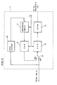
- Fig. 1 is a block diagram schematically explaining signal flow in a reproduction system of a VTR in which such a distortion compensating circuit is used.
- Four channel video signals reproduced from a magnetic tape 1 by four magnetic heads 2a through 2d are respectively amplified by the corresponding reproducing amplifiers 3a through 3d, and then the amplified reproduced video signals are applied to an equalizer and RF switching circuit 4 wherein the signals are converted into sequential signals of two channels.
- the two channel reproduced video signals are applied to an FM demodulator 5, wherein they are FM demodulated.
- the reproduced video signals FM demodulated by the FM demodulator 5 are applied to a time base corrector (TBC) 6, wherein they are converted into digital signals and time bases thereof are corrected.
- TBC time base corrector
- the reproduced video signals converted into the digital signals in the TBC 6 are applied to a distortion compensating circuit (or a digital level compensating circuit DLC) 7.
- the distortion compensating circuit 7 compensates nonlinear distortion of the reproduced video signals.
- dropout of the reproduced signals is compensated by a dropout compensating circuit (DOC) 9 and at the same time, the signals are reconverted into analog signals and outputted as a luminance signal Y and two color signals P B and P R .
- DOC dropout compensating circuit
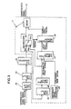
- Fig. 2 is a schematic block diagram showing the structure of the distortion compensating circuit 7 shown in Fig. 1.
- the distortion compensating circuit 7 receives a digital reproduced video signal applied from the TBC 6 of Fig. 1.
- This reproduced video signal is applied to a gate circuit 10, wherein input ramp signals Ln included in respective blanking periods of the reproduced video signal are extracted, and then the extracted input ramp signals Ln are applied to an averaging circuit 11.
- the averaging circuit 11 averages input ramp signals of several fields in response to time base signals Tn supplied from a time base signal source (not shown) in order to reduce noise components included in the reproduced ramp signals and applies the result thereof as a data signal to an RAM 12.
- the time base signals Tn are applied to an address input of the RAM 12 and consequently, while being addressed by the time base signals Tn, the RAM 12 stores the averaged input ramp signals as data signals.
- the data signal outputted from the RAM 12 is applied to an address input of an RAM 13 through a switch 15 switched to a terminal 15a during a blanking period of the reproduced video signal, while the time base signal Tn is applied to the data input of the RAM 13.
- the RAM 13 stores the time base signal Tn as a data signal during the blanking period of the reproduced video signal. Namely, the information for compensating nonlinear distortion based on the input ramp signals is stored in the RAM 13.
- the reproduced video signal from the TBC 6 is applied to the address input of the RAM 13 through the switch 15 switched to a terminal 15b during a non-blanking period of the reproduced video signal.
- the RAM 13 outputs the stored data.
- the data signals outputted from the RAM 13 are applied to an address input of an ROM 14 and while using the data signals as address signals, the ROM 14 outputs data signals indicative of levels corresponding to the respective addresses.
- the RAM 12 stores the input ramp signals subjected to nonlinear distortion while using the time base signals Tn as address signals and the RAM 13 stores the time base signals Tn while using the data signals corresponding to the input ramp signals as an address signals in such a manner that the address and the data are inverted with respect to the RAM 12. Then, by outputting the data signal corresponding to the time base signal Tn from the RAM 13 while using the reproduced video signal subjected to the nonlinear distortion as the address signal, the data signal which nonlinear distortion is compensated can be obtained.
- the conventional distortion compensating circuit shown in Fig. 2 requires two RAMs 12 and 13 and one ROM 14. These RAMs and ROM require large storage capacities for storing data corresponding to the whole input ramp signal. More specifically, assuming that the input video signal to the distortion compensating circuit is a digital signal of n bits, at least a capacity of n x 2 n bits is required. Therefore, such a conventional distortion compensating circuit as shown in Fig. 2 is difficult to be made smaller and reducing the manufacturing cost thereof is very difficult. Particularly, such problems are acute for a distortion compensating circuit for processing video signals of multiple channels.
- an object of the present invention is to provide a compact and inexpensive distortion compensating circuit.
- Another object of the present invention is to reduce a capacity of storing means for use in a distortion compensating circuit.
- the present invention is directed to a distortion compensating circuit in which a difference between an input reference signal and a comparison reference signal, that is, a compensation data signal corresponding to the magnitude of nonlinear distortion of the input signal, is computed, this compensation data signal is stored in a memory, using the input reference signal as an address signal, the compensation data signal is further read out using the input signal as an address signal, so that the read compensation data signal is added to the input signal.
- a main advantage of the present invention is that not the entire input reference signal but only a difference component between the input reference signal and the comparison reference signal needs to be stored, so that a required storage capacity can be drastically reduced.
- Fig. 3 shows a distortion compensating circuit 7 according to one embodiment of the present invention, which is supposed to be interposed between the TBC 6 and the TCI decoder 8 in the reproduction system of the VTR as in Fig. 1.
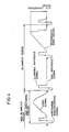
- the applied reproduced video signal includes a ramp signal which level varies in the range that a video signal can cover as an input reference signal in the blanking period as shown in Fig. 4.
- the reproduced video signal includes a clamping reference signal indicative of the intermediate level of the video signal and an AGC reference signal for use in setting the amplitude of the reproduced video signal, as shown in Fig. 4.
- a clamp circuit 22, an AGC circuit 23 and an A/D convertor 24 are elements provided in the TBC 6 of Fig. 1.
- the clamp circuit 22 samples the clamping reference signals of Fig. 4 at the same rate as that of a horizontal synchronizing frequency and sets a direct current level of the reproduced video signal to a predetermined level.
- the AGC circuit 23 detects a difference between a level of the AGC reference signal of the reproduced video signal of Fig. 4 and a level of the above-described clamping reference signal to set the amplitude of the reproduced video signal such that the difference attains a predetermined value.
- the AGC reference signal such a signal as indicating a black level during one horizontal period is used.
- the clamp circuit 22 and the AGC circuit 23 adjust the level of the reproduced video signal so as to be in the range of the A/D conversion by the A/D convertor 24.
- the reproduced video signal can take any value represented by the predetermined number of bits and consequently no saturation of the reproduced video signal occurs.
- the reproduced video signal inputted to A/D convertor 24 is converted every predetermined period into a digital signal comprising data indicative of the level of the inputted reproduced video signal. While in the embodiment of Fig.
- the output of the A/D convertor 24 is applied to an adder 31, one input terminal 30a of a multiplexer 30 and a gate circuit 25 in the distortion compensating circuit 7.
- the gate circuit 25 extract the input ramp signal as an input reference signal included in the blanking period of the reproduced video signal and applies the same to an averaging circuit 26.
- the averaging circuit 26 averages a signal level value of each of about 16 input ramp signals with respect to the same phase. As a result, the noise components in the input ramp signal is reduced to prevent reduction of an S/N ratio of a reproduced signal caused by compensation.
- the output of the averaging circuit 26 is applied to a negative input of a subtracting circuit 27 and also to the other input terminal 30b of the multiplexer 30.
- the positive input of the subtracting circuit 27 receives a comparing ramp signal as a comparison reference signal generated in a reference signal generator 28.
- the comparing ramp signal has the same waveform as that of the original recording ramp signal included in the video signal when the video signal is recorded on a recording medium.
- the substracting circuit 27 outputs the data corresponding to a difference between the input ramp signal inputted to the negative input and the comparing ramp signal inputted to the positive input as described above, as a compensation data signal and applies the same as a data signal to a compensating memory 29.
- the address input of the compensating memory 29 receives a signal outputted from a terminal 30C of the multiplexer 30 as an address signal.
- the multiplexer 30 selects the signal inputted to the terminal 30b and applies the same to the compensating memory 29 during the blanking period of the reproduced video signal, and selects the signal inputted to the terminal 30a and applies the same to the compensating memory 29 during the non-blanking period of the reproduced video signal.
- the compensating memory 29 stores the compensation data signal outputted from the subtracting circuit 27, using the input ramp signal outputted from the averaging circuit 26 as an address signal during the blanking period of the reproduced video signal, it outputs the stored compensation data signal, using the reproduced video signal from the A/D convertor 24 as an address signal during the non-blanking period of the reproduced video signal.
- the compensation data signal outputted from the compensating memory 29 is added to the reproduced video signal from the A/D convertor 24 by the adder 31. Then, the output of the adder 31 is supplied as the compensated reproduced video signal from the distortion compensating circuit 7.
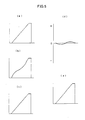
- Fig. 5 shows waveform diagrams explaining operations of the embodiment shown in Fig. 3.
- description will be made of the principle of the distortion compensating operation performed by the distortion compensating circuit 7 shown in Fig. 3 in which a video signal is reproduced which is recorded on a magnetic tape with a recording ramp signal having such waveform as shown in Fig. 5 (a) included in the blanking period.
- the reproduced video signal includes an input ramp signal which waveform is distorted as shown in, for example, Fig. 5 (b) due to the characteristics of an FM modulator, an FM demodulator and an amplifier of VTR and the like.
- the reproduced video signal is converted into a digital signal comprising data indicative of the level of the reproduced video signal by the A/D convertor 24.
- the reference signal generator 28 generates a comparing ramp signal comprising the data having the same waveform as that of the recording ramp signal included in the video signal when the video signal is recorded, in synchronization with the input ramp signal, as shown in Fig. 5 (c).
- the input ramp signal and the comparing ramp signal are subtracted by the subtracting circuit 27, thereby obtaining a compensation data signal comprising the data having such a waveform of the distortion component as shown in Fig. 5 (d).
- This compensation data signal is stored in the compensating memory 29, using the input ramp signal inputted from the averaging circuit 26 as an address signal by connecting the terminal 30b to the terminal 30c of the multiplexer 30 during the blanking period of the reproduced video signal.
- the compensation data signals are also stored in the discontinuous address portions by interpolation or the like.
- the above-described compensation data signal comprises only the data having the waveform of the distortion components, the range of value that the compensation data signal can cover is quite narrow as compared with that the input ramp signal can cover. Therefore, the storage capacity of the compensating memory 29 for storing the compensation data signal can be smaller than that of each memory in the conventional example of Fig. 2. Besides, since with respect to the compensation data signal, the input ramp signal inputted from the A/D convertor 24 through the gate circuit 25 and the averaging circuit 26 is directly stored as a data signal in the compensating memory 29, unlike the conventional example of Fig. 2, additional memories and the like are not required for inverting the addresses and the data.
- the reproduced video signal outputted from the A/D convertor 24 is applied as an address signal to the address input of the compensating memory 29 by connecting the terminal 30a to the terminal 3oC of the multiplexer 30.
- the compensating memory 29 outputs the compensation data signal corresponding to the data indicative of the level of the reproduced video signal and applies the same to one input of the adder 31 during the non-blanking period of the reproduced video signal.
- the other input of the adder 31 directly receives the reproduced video signal outputted from the A/D convertor 24 and adds the same to the above-described compensation data signal.
- the compensated video signal having the data indicative of the level at which distortion is compensated is outputted from the adder 31. While in the example of Fig. 5, for convenience sake, the description is made of a case in which the reproduced video signal having the same waveform as that of the input ramp signal is subjected to the distortion compensation, the same distortion compensation may be carried out for video signals having various waveforms in each horizontal period of Fig. 4.
- the storage capacity of the compensating memory 29 can be reduced, for example, to or less than about 1/3 as compared with such a case where the input ramp signal itself is stored as the conventional example of Fig. 2. Besides, only one compensating memory is required.
- Fig. 6 is a block diagram showing a distortion compensating circuit according to another embodiment of the present invention.
- the embodiment of Fig. 6 shows the distortion compensating circuit for compensating distortion of video signals of two channels A and B.
- reproduced video signals of the A and B channels are applied to the distortion compensating circuit 7 from an A/D convertor 24a and an A/D convertor 24b, respectively.
- Both the reproduced video signals of the A channel and the B channel are applied to a gate circuit 25 whereby input ramp signals of the A and B channels are sequentially extracted in a time divisional manner, and the extracted input ramp signals are applied to an averaging circuit 26.
- the following operation is basically the same as that of the embodiment shown in Fig.
Landscapes
- Engineering & Computer Science (AREA)
- Multimedia (AREA)
- Signal Processing (AREA)
- Picture Signal Circuits (AREA)
- Television Signal Processing For Recording (AREA)
- Analogue/Digital Conversion (AREA)
Applications Claiming Priority (2)
| Application Number | Priority Date | Filing Date | Title |
|---|---|---|---|
| JP216919/89 | 1989-08-23 | ||
| JP1216919A JP2522551B2 (ja) | 1989-08-23 | 1989-08-23 | 映像信号の歪補正装置 |
Publications (3)
| Publication Number | Publication Date |
|---|---|
| EP0414556A2 true EP0414556A2 (fr) | 1991-02-27 |
| EP0414556A3 EP0414556A3 (en) | 1992-07-22 |
| EP0414556B1 EP0414556B1 (fr) | 1996-11-06 |
Family
ID=16695981
Family Applications (1)
| Application Number | Title | Priority Date | Filing Date |
|---|---|---|---|
| EP90309290A Expired - Lifetime EP0414556B1 (fr) | 1989-08-23 | 1990-08-23 | Circuit de compensation pour compenser les distorsions d'un signal vidéo en détectant les distorsions d'un signal en rampe dans le signal vidéo |
Country Status (4)
| Country | Link |
|---|---|
| US (1) | US5119194A (fr) |
| EP (1) | EP0414556B1 (fr) |
| JP (1) | JP2522551B2 (fr) |
| DE (1) | DE69029070T2 (fr) |
Families Citing this family (5)
| Publication number | Priority date | Publication date | Assignee | Title |
|---|---|---|---|---|
| KR930003990Y1 (ko) * | 1990-07-06 | 1993-06-25 | 삼성전자 주식회사 | 색신호 재생회로 |
| JP3041118B2 (ja) * | 1991-09-30 | 2000-05-15 | 株式会社東芝 | 磁気記録再生装置 |
| US6587984B1 (en) | 1997-03-18 | 2003-07-01 | Nippon Columbia Co., Ltd. | Distortion detecting device, distortion correcting device, and distortion correcting method for digital audio signal |
| US6337676B1 (en) * | 1998-03-30 | 2002-01-08 | Kabushiki Kaisha Toshiba | Flat-panel display device |
| JP4827524B2 (ja) * | 2005-12-26 | 2011-11-30 | キヤノン株式会社 | 撮像装置 |
Family Cites Families (7)
| Publication number | Priority date | Publication date | Assignee | Title |
|---|---|---|---|---|
| FR2501941B1 (fr) * | 1981-03-12 | 1986-04-11 | Cit Alcatel | Procede et dispositif d'accentuation des traits d'une image en noir et blanc reproduite a partir d'une transcription numerique |
| GB2113051A (en) * | 1981-12-04 | 1983-07-27 | Philips Electronic Associated | Data pulse waveform shaper |
| JPS61290822A (ja) * | 1985-06-19 | 1986-12-20 | Oki Electric Ind Co Ltd | 温度センサの直線化方式 |
| KR910001466B1 (ko) * | 1985-07-12 | 1991-03-07 | 마쯔시다덴기산교 가부시기가이샤 | 영상신호의 신호처리장치 |
| JPS6310982A (ja) * | 1986-07-02 | 1988-01-18 | Matsushita Electric Ind Co Ltd | 映像信号の信号処理装置 |
| EP0321181B1 (fr) * | 1987-12-14 | 1994-03-09 | Mitsubishi Denki Kabushiki Kaisha | Dispositif de correction des characteristiques |
| US4991021A (en) * | 1988-06-22 | 1991-02-05 | Nec Corporation | Digital video signal compensation circuit |
-
1989
- 1989-08-23 JP JP1216919A patent/JP2522551B2/ja not_active Expired - Lifetime
-
1990
- 1990-08-17 US US07/570,151 patent/US5119194A/en not_active Expired - Fee Related
- 1990-08-23 EP EP90309290A patent/EP0414556B1/fr not_active Expired - Lifetime
- 1990-08-23 DE DE69029070T patent/DE69029070T2/de not_active Expired - Fee Related
Also Published As
| Publication number | Publication date |
|---|---|
| US5119194A (en) | 1992-06-02 |
| JP2522551B2 (ja) | 1996-08-07 |
| EP0414556B1 (fr) | 1996-11-06 |
| JPH0380621A (ja) | 1991-04-05 |
| EP0414556A3 (en) | 1992-07-22 |
| DE69029070D1 (de) | 1996-12-12 |
| DE69029070T2 (de) | 1997-03-27 |
Similar Documents
| Publication | Publication Date | Title |
|---|---|---|
| US4258384A (en) | Color video signal processing system | |
| US5038219A (en) | Video signal recording apparatus | |
| CA1160338A (fr) | Dispositif de compensation des erreurs de vitesse pour la correction des erreurs de base de temps de signaux d'information periodiques | |
| EP0171759B1 (fr) | Dispositif de traitement de signal pour compenser la distorsion dans un signal transmis ou enregistré | |
| KR920003937B1 (ko) | VTR 기록재생 영상신호의 지터(jitter) 검출방법 및 검출장치 | |
| KR910001466B1 (ko) | 영상신호의 신호처리장치 | |
| US5119194A (en) | Compensating circuit for compensating distortion of video signal by detecting distortion of ramp signal in video signal | |
| US4628369A (en) | Video signal dropout compensation circuit | |
| US5067031A (en) | Method and apparatus for processing video signals recorded on or recovered from magnetic media | |
| KR940009542B1 (ko) | 시간축 보정 장치 및 속도 에러 보정 회로 | |
| EP0432668B1 (fr) | Appareil et procédé pour le traitement du signal vidéo pour la compensation de la base de temps | |
| EP0438293B1 (fr) | Dispositif d'enregistrement/de reproduction de signal vidéo comportant une fonction de compensation de perte de signal | |
| US5438558A (en) | Image signal apparatus including clamping processing of image signal | |
| JP2805772B2 (ja) | 映像信号記録回路 | |
| US5162921A (en) | Clamp for video signal processing circuit | |
| EP0321181B1 (fr) | Dispositif de correction des characteristiques | |
| JPH0533878B2 (fr) | ||
| JPH0353792A (ja) | 磁気記録再生装置 | |
| JPS61234679A (ja) | 映像信号の信号処理装置 | |
| JPH0353791A (ja) | 磁気記録再生装置 | |
| JPH0353790A (ja) | 磁気記録再生装置 | |
| EP0484144A2 (fr) | Procédés et dispositif de traitement d'un signal vidéo | |
| JPH0417512B2 (fr) | ||
| JPH02210665A (ja) | 信号処理回路 | |
| JPH0787524A (ja) | 映像信号再生装置 |
Legal Events
| Date | Code | Title | Description |
|---|---|---|---|
| PUAI | Public reference made under article 153(3) epc to a published international application that has entered the european phase |
Free format text: ORIGINAL CODE: 0009012 |
|
| 17P | Request for examination filed |
Effective date: 19901214 |
|
| AK | Designated contracting states |
Kind code of ref document: A2 Designated state(s): DE FR GB |
|
| PUAL | Search report despatched |
Free format text: ORIGINAL CODE: 0009013 |
|
| AK | Designated contracting states |
Kind code of ref document: A3 Designated state(s): DE FR GB |
|
| 17Q | First examination report despatched |
Effective date: 19940713 |
|
| RAP1 | Party data changed (applicant data changed or rights of an application transferred) |
Owner name: SHARP KABUSHIKI KAISHA |
|
| GRAH | Despatch of communication of intention to grant a patent |
Free format text: ORIGINAL CODE: EPIDOS IGRA |
|
| GRAH | Despatch of communication of intention to grant a patent |
Free format text: ORIGINAL CODE: EPIDOS IGRA |
|
| GRAA | (expected) grant |
Free format text: ORIGINAL CODE: 0009210 |
|
| AK | Designated contracting states |
Kind code of ref document: B1 Designated state(s): DE FR GB |
|
| REF | Corresponds to: |
Ref document number: 69029070 Country of ref document: DE Date of ref document: 19961212 |
|
| ET | Fr: translation filed | ||
| PLBE | No opposition filed within time limit |
Free format text: ORIGINAL CODE: 0009261 |
|
| STAA | Information on the status of an ep patent application or granted ep patent |
Free format text: STATUS: NO OPPOSITION FILED WITHIN TIME LIMIT |
|
| 26N | No opposition filed | ||
| PGFP | Annual fee paid to national office [announced via postgrant information from national office to epo] |
Ref country code: FR Payment date: 20010810 Year of fee payment: 12 |
|
| PGFP | Annual fee paid to national office [announced via postgrant information from national office to epo] |
Ref country code: DE Payment date: 20010813 Year of fee payment: 12 |
|
| PGFP | Annual fee paid to national office [announced via postgrant information from national office to epo] |
Ref country code: GB Payment date: 20010822 Year of fee payment: 12 |
|
| REG | Reference to a national code |
Ref country code: GB Ref legal event code: IF02 |
|
| PG25 | Lapsed in a contracting state [announced via postgrant information from national office to epo] |
Ref country code: GB Free format text: LAPSE BECAUSE OF NON-PAYMENT OF DUE FEES Effective date: 20020823 |
|
| PG25 | Lapsed in a contracting state [announced via postgrant information from national office to epo] |
Ref country code: DE Free format text: LAPSE BECAUSE OF NON-PAYMENT OF DUE FEES Effective date: 20030301 |
|
| GBPC | Gb: european patent ceased through non-payment of renewal fee |
Effective date: 20020823 |
|
| PG25 | Lapsed in a contracting state [announced via postgrant information from national office to epo] |
Ref country code: FR Free format text: LAPSE BECAUSE OF NON-PAYMENT OF DUE FEES Effective date: 20030430 |
|
| REG | Reference to a national code |
Ref country code: FR Ref legal event code: ST |