EP0414988A2 - Système d'affichage - Google Patents
Système d'affichage Download PDFInfo
- Publication number
- EP0414988A2 EP0414988A2 EP90102505A EP90102505A EP0414988A2 EP 0414988 A2 EP0414988 A2 EP 0414988A2 EP 90102505 A EP90102505 A EP 90102505A EP 90102505 A EP90102505 A EP 90102505A EP 0414988 A2 EP0414988 A2 EP 0414988A2
- Authority
- EP
- European Patent Office
- Prior art keywords
- display
- control means
- display panel
- turn
- display control
- Prior art date
- Legal status (The legal status is an assumption and is not a legal conclusion. Google has not performed a legal analysis and makes no representation as to the accuracy of the status listed.)
- Granted
Links
Images


Classifications
-
- G—PHYSICS
- G06—COMPUTING OR CALCULATING; COUNTING
- G06F—ELECTRIC DIGITAL DATA PROCESSING
- G06F3/00—Input arrangements for transferring data to be processed into a form capable of being handled by the computer; Output arrangements for transferring data from processing unit to output unit, e.g. interface arrangements
- G06F3/14—Digital output to display device ; Cooperation and interconnection of the display device with other functional units
- G06F3/147—Digital output to display device ; Cooperation and interconnection of the display device with other functional units using display panels
-
- G—PHYSICS
- G09—EDUCATION; CRYPTOGRAPHY; DISPLAY; ADVERTISING; SEALS
- G09G—ARRANGEMENTS OR CIRCUITS FOR CONTROL OF INDICATING DEVICES USING STATIC MEANS TO PRESENT VARIABLE INFORMATION
- G09G3/00—Control arrangements or circuits, of interest only in connection with visual indicators other than cathode-ray tubes
- G09G3/20—Control arrangements or circuits, of interest only in connection with visual indicators other than cathode-ray tubes for presentation of an assembly of a number of characters, e.g. a page, by composing the assembly by combination of individual elements arranged in a matrix no fixed position being assigned to or needed to be assigned to the individual characters or partial characters
- G09G3/34—Control arrangements or circuits, of interest only in connection with visual indicators other than cathode-ray tubes for presentation of an assembly of a number of characters, e.g. a page, by composing the assembly by combination of individual elements arranged in a matrix no fixed position being assigned to or needed to be assigned to the individual characters or partial characters by control of light from an independent source
- G09G3/36—Control arrangements or circuits, of interest only in connection with visual indicators other than cathode-ray tubes for presentation of an assembly of a number of characters, e.g. a page, by composing the assembly by combination of individual elements arranged in a matrix no fixed position being assigned to or needed to be assigned to the individual characters or partial characters by control of light from an independent source using liquid crystals
-
- G—PHYSICS
- G09—EDUCATION; CRYPTOGRAPHY; DISPLAY; ADVERTISING; SEALS
- G09G—ARRANGEMENTS OR CIRCUITS FOR CONTROL OF INDICATING DEVICES USING STATIC MEANS TO PRESENT VARIABLE INFORMATION
- G09G2310/00—Command of the display device
- G09G2310/02—Addressing, scanning or driving the display screen or processing steps related thereto
- G09G2310/0232—Special driving of display border areas
Definitions
- the present invention relates to a display system to display image data by using a liquid crystal display panel in which scan signal lines and information signal lines are arranged like a matrix and a liquid crystal having a memory performance is sandwiched between the scan signal lines and the information signal lines.
- a CRT such as Multisync II, Multisync 3D, 4D, or 5D made by NEC Ltd., or the like has been konwn as a product in which it is possible to display in many display modes by a single display.
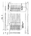
- Table 1 in Fig. 8 shows video modes (display modes) which are supported by the Multisync 4D and 5D.
- the principle of the fundamental operation of the display having the memory performance such as a ferroelectric liquid crystal display or the like differs from various fundamental operation principles which are used in the conventional displays such as CRT, STN-LCD (super twisted liquid crystal display), and PDP (plasma display). Therefore, the partial writing scanning method using the memory performance which has been proposed so far by Kanbe et al. in U.S.P. No. 4,655,561 is intended to be realized by the method of realizing "low frame frequency driving + partial writing scanning" to execute the display at a high resolution by the liquid crystal display having the memory performance in JP-A-63-65494, the Official Gazette of Japanese Patent Application No. 63-285141, etc. which have been proposed by the inventors et al. of the present invention.
- a method of realizing the above object of the present invention will now be clarified hereinbelow by providing a whole construction and its control method for supporting various display modes for use in, particularly, the PC/AT machine made by IBM Corporation and also for supporting a high precision mode of a resolution of 1280 (dots) x 1024 (dots) by using the ferroelectric liquid crystal display as an example.
- the ferroelectric liquid crystal display as a representative example of the display having the memory performance has a temperature dependency of the driving conditions which is represented in Fig. 2.
- Fig. 2 shows that a frame frequency is set to 7 Hz at 10 °C, 10 Hz at 25 °C, and 20 Hz at 40 °C (the number of scan lines: 1024, driving voltage: 24 V, KMT-408 made by Nippon Nitrogen Co., Ltd. was used).
- the flicker can be prevented by an interlacing process of eight scan lines in the low frame frequency driving which has already been proposed.
- the flicker can be sufficiently prevented by executing the interlacing process of four scan lines.
- a division phenomenon of the display screen upon display of an animation screen for instance, upon scroll display or the like which is only one drawback in the interlacing process of eight scan lines can be also reduced.
- the driving method further changes depending on the video mode. For instance, in the FLC display at 10 Hz in the foregoing display mode of 1024 scan lines in Table 1 in Fig.
- the number of scan lines is set to 480 in the VGA display mode and the frame frequency is set to 20 Hz or higher.
- the flicker can be sufficiently prevented by the ordinary (two scan lines) interlacing process and the division of the screen upon animation display can be further reduced.
- a method of determining the display mode exists, a method which can change the frame frequency of the display together with the environmental temperature of the display does not exist.
- the FLC display is the X-Y matrix display as mentioned above, the change in number of pixels depending on the display mode cannot be realized by a simple method such that a beam frequency of the CRT display is changed.
- the physical number of pixels in the X-Y matrix display is unconditionally determined at the time of production and cannot be changed. Therefore, there occurs a necessity to convert the logic number of pixels which is required in the display mode into the physical number of pixels.
- the input data side requested 256 gradient levels with respect to each of R, G, and B, the relations among the colors and the numbers of gradient levels of the input data and output data must be previously determined in correspondence to each display mode.
- an effective display area and an external frame portion of the effective display area exist in the display area on the display.
- the portion which is surrounded by a point (x1, y1) and a point (x2, y2) which are away from the physical coordinate origin (x0, y0) on the display is used as an effective display screen.
- the logic screen area which is required by the display mode is set to the effective display area.
- the VGA display mode area of 640 (in the x direction) x 480 (in the y direction) in the physical screen display of 1280 (x direction) x 1024 (y direction) the following two cases are considered and the external frame sizes differ.
- the external frame portion of the effective display portion of the display having the memory performance such as an FLC display must be driven by predetermined display data and such a point is different from the conventional display.
- the display state of the frame portion is not aligned to, for instance, either white or black because of the memory performance. Therefore, when the display mode is decided, the size, color, and gradient level of the frame portion must be determined and in addition to the image data, the frame portion drive data must be generated for display.
- the display which is connected has two functions for the ordinary CRT or the like and for the FLC display
- the system must be constructed in a manner such that when the user changed the connection to exchange the display or the like, the data transfer method and data transfer format of a graphics adapter can be changed.
- the data transfer method and data transfer format of the FLC display in the foregoing patent essentially differ from those of the conventional CRT or the like.
- the FLC display Since the FLC display has the memory performance, an attention needs to be paid upon turn-on, resetting, and turn-off of the power source. For instance, with respect to the orientation control of the FLC display, if the supply of a DC voltage is not avoided as possible, an orientation deterioration and an after-image for a long time called a sticking" phenomenon occur. Therefore, a drive control circuit must be designed so as to avoid such a DC voltage supply upon turn-on or turn-off of the power source.
- the drive control circuit is integrated with a computer, in many cases, generally, the power source is supplied from the main body side and the power source is also turned on or off by the user from the main body side. Therefore, it is necessary that the power on/off from the user side is informed to the drive control circuit of the FLC display and a predetermined on/off control necessary for the FLC display is executed and, thereafter, the ordinary power on/off control is performed.
- ROM BIOS an ROM BIOS
- the ROM BIOS actually executes the interface regarding the control and display of the computer main body and FLC display. The user can control the display mode or the like without needing the detailed knowledge, particularly, to control and drive the FLC display.
- the second object of the invention is to provide a display system using a liquid crystal display panel having the memory performance, in which driving conditions of the liquid crystal display panel can be properly determined upon turn-on or resetting of a power source of the system.
- the third object of the invention is to provide a display system using a liquid crystal display panel having the memory performance, in which driving conditions of the liquid crystal display panel can be properly determined in correspondence to a change in environmental temperature.
- the fourth object of the invention is to provide a display system using a liquid crystal display panel having the memory performance, in which information necessary to drive the liquid crystal display panel is previously stored as display modes in memory means and the liquid crystal display panel is driven and controlled in accordance with the display mode.
- the fifth object of the invention is to provide a display system using a liquid crystal display panel having the memory performance, in which the user can totally control the image display in accordance with various display modes under control of a host computer.
- Fig. 1 shows a construction of each hardware of a display panel 2 (1280 x 1024 pixels), display drivers 3 and 4, a display unit controller 8, and a graphics controller 9 having a VRAM 10 as an image data storage memory which construct a display system using a ferroelectric liquid crystal display according to an embodiment of the present invention.
- Fig. 1 also shows a hardware construction of a host CPU 11 and a host bus 12 showing the PC/AT machine made by IBM Corporation.
- Fig. 1 also shows an ROM BIOS 13 having therein a whole control monitor program as the present invention.
- Host bus Standard interface hardware bus which is specified by IBM Corporation and is called an AT bus in the PC/AT machine made by IBM Corporation.
- the function which was defined in the ROM BIOS 13 is called from the video data generating side, that is, from the host CPU 11 side in accordance with a predetermined calling rule. If necessary parameters which are necessary to realize the function are transmitted to the graphics controller 9. If the function was called by a normal procedure, in order to realize the requested function, the translation is made by a GCPU (graphics control central processing unit) 14 or the graphics controller 9 is directly accessed.
- GCPU graphics control central processing unit
- the graphics controller 9 transfers the drive data and video data to the FLC display unit by use of bidirectional data buses PD0 to PD7.
- An AH/DL signal is used to distinguish time. When the AH/DL signal is set to the High level, the data on the PD0 to PD7 indicates the "drive data”. If the AH/DL signal is at the low level, the data indicates the "video data”.
- the FLC display unit controller 8 extracts the drive data from the video signal with the drive data which is transferred as the data on the PD0 to PD7 and executes the process based on the drive data. On the other hand, the video data is sent to a shift register 6 on the information electrode drive circuit side on the basis of transfer clocks.
- the driving and display of the FLC display and the generation of the drive data and video data in the graphics controller 9 are asynchronously executed, it is necessary to synchronize the apparatuses upon transmission of the display data.
- the signals Hsync and Vsync are used to realize such synchronization.
- the Hsync signal is generated in the FLC display unit controller 8 every horizontal scan period, while the Vsync signal is generated in the controller 8 every vertical scan period upon refreshing.
- the Hsync and Vsync signals are sent to the graphics controller 9.
- the graphics controller 9 always monitors the Hsync and Vsync signals.
- the display data (drive data + video data) is transferred.
- the graphics controller 9 waits until the next transfer permission signal is input.
- Fig. 4 is a timing chart for the fundamental communication when the display data is sent from the graphics controller 9 side to the FLC display unit controller 8 side of an FLC display unit 1. The operation will now be described.
- the display controller 8 of the FLC display unit 1 sets the Hsync to the High level during the display data transfer period of time. After completion of a series of processes based on the transferred drive data, the controller 8 of the FLC display 1 again sets the Hsync to the Low level and enters the standby mode to receive the next display data.
- Fig. 5 is a timing chart for the fundamental communication when the graphics controller 9 side reads out the display data from the controller 8 side of the FLC display unit 1. The operation will now be described hereinbelow.
- the graphics controller 9 sends "information read request data" which has been predetermined between the controller 8 of the FLC display unit 1 and the controller 9 as the drive data to the controller 8 of the FLC display unit 1 at the timings of A0 to A15 in Fig. 5.
- the graphics controller 9 sets the IH/OL signal to the High level, thereby setting the data input mode.
- the data buses PD0 to PD7 are set in the high impedance state (Z) when they are seen from the side of the graphics controller 9.
- the controller 8 of the FLC display unit 1 recognizes the "information read request data"
- it confirms that the IH/OL line is at the High level and, thereafter, the controller 8 sends the data onto the data buses PD0 to PD7 and, further, sets the FLG signal to the High level.
- the graphics controller 9 detects that the FLG line is set to the High level, it reads the data how existing on the data buses PD0 to PD7 and stores into the GCPU 14.
- the display data is sent from the graphics controller 9 side to the display side in a manner similar to the case of the communication in Fig. 4.
- the scan line address data is used as the drive data and is sent to the positions of A0 to A15 in Fig. 4 and is transferred to the display controller 8.
- the scan line address data is extracted by the controller 8 of the FLC display unit 1 and is input to a decoder 7 on the scan line electrode drive circuit side in accordance with the timing to drive the designated scan line, so that the designated scan line on the display is selected.
- the video data is transferred to the shift register 6 on the information electrode drive circuit side and is shifted on an 8-pixel unit basis by transfer clocks (CLK).
- CLK transfer clocks
- the video data of 1280 pixels is transferred to a line memory 5 provided for the shift register 6 and is stored for one horizontal scan period of time.
- the controller 8 of the display unit again sets the Hsync to the Low level and receives the display data of the next scan line.
- the display mode for the display is fundamentally set and changed on the basis of a request from the host side and fundamentally in accordance with a timing chart shown in Fig. 6. Explanation will now be made practically hereinbelow.
- the controller 8 side of the display unit 1 cannot know in which display mode the graphics controller 9 has already been operating.
- the controller 8 of the display unit 1 sends the INT signal to the graphics controller 9 and requests to set the display mode.
- the graphics controller 9 receives the INT signal from the display unit controller 8, it checks the FLG line. If the FLG line is at the Low level, the graphics controller 9 recognizes that the setting of the display mode is requested. Subsequently, the display mode is set in accordance with a procedure similar to the case of the step (4) for the operation upon setting of the display mode - the operation upon setting from the host side.
- a read request can be also sent from the display side to the main apparatus as necessary.
- the display in a manner similar to the case of setting the display mode, the display first sends the INT signal to the graphics controller 9.
- the graphics controller 9 receives the INT signal from the display side, it checks the FLG line. If the FLG line is at the High level, the graphics controller 9 recognizes that the reading of the temperature data is requested. After that, the reading process of the temperature data is executed in a manner similar to the case where the requested was generated from the main apparatus side.
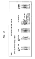
- Table 2 shows the adapter names and resolutions which are supported in the 1. Alphanumeric mode and the 2. Graphics mode in the IBM mode, the colors, the numbers of gradient levels, and the FLC display drive data.
- an expression “b/p” is used to decide the color and the number of gradient levels in the output data for the input data.
- the expression "b/p” represents the color for one pixel (one logical pixel) and the number of bits indicative of the binarization expression of the gradient data amount.
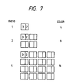
- An expression “ratio” in Table 2 indicates the relation between the number of physical pixels and the number of logical pixels and the relation is shown in Fig. 7.
- the FLC display is fundamentally a binary expression display and a method in which two physical pixels having different area ratios are set into one pixel unit as mentioned above has already been proposed as one of methods of realizing the multi-value expression by the FLC display, namely, the gradation expression.
- either one of various display modes is used from the time of the turn-on of the power source and the total control method which is inevitable to change the display mode in accordance with the necessity is set in the ROM.
- a control monitor section in which the display mode can be also further changed from the host side in accordance with a predetermined procedure as necessary.
- the invention is not limited to the ferroelectric liquid crystal display but can be obviously applied to the display system which has a memory performance and in which the driving conditions include the temperature tendency.
- the display system includes memory means for storing image data to be displayed by the display panel, display mode memory means for storing a display mode as a driving condition of the display panel with respect to the image data to be displayed by the display panel, and display control means for reading out the image data to be displayed from the memory means, for controlling the drive control means in accordance with the display mode stored in the display mode memory means.
Landscapes
- Engineering & Computer Science (AREA)
- Theoretical Computer Science (AREA)
- Physics & Mathematics (AREA)
- General Physics & Mathematics (AREA)
- Crystallography & Structural Chemistry (AREA)
- Computer Hardware Design (AREA)
- Chemical & Material Sciences (AREA)
- General Engineering & Computer Science (AREA)
- Human Computer Interaction (AREA)
- Liquid Crystal Display Device Control (AREA)
- Control Of Indicators Other Than Cathode Ray Tubes (AREA)
- Alarm Systems (AREA)
- Input Circuits Of Receivers And Coupling Of Receivers And Audio Equipment (AREA)
- Selective Calling Equipment (AREA)
- Liquid Crystal (AREA)
Applications Claiming Priority (2)
| Application Number | Priority Date | Filing Date | Title |
|---|---|---|---|
| JP01226632A JP3126360B2 (ja) | 1989-09-01 | 1989-09-01 | 表示システム及びその表示制御方法 |
| JP226632/89 | 1989-09-01 |
Publications (3)
| Publication Number | Publication Date |
|---|---|
| EP0414988A2 true EP0414988A2 (fr) | 1991-03-06 |
| EP0414988A3 EP0414988A3 (en) | 1992-09-09 |
| EP0414988B1 EP0414988B1 (fr) | 1997-06-11 |
Family
ID=16848228
Family Applications (1)
| Application Number | Title | Priority Date | Filing Date |
|---|---|---|---|
| EP90102505A Expired - Lifetime EP0414988B1 (fr) | 1989-09-01 | 1990-02-08 | Système d'affichage |
Country Status (7)
| Country | Link |
|---|---|
| US (1) | US5784037A (fr) |
| EP (1) | EP0414988B1 (fr) |
| JP (1) | JP3126360B2 (fr) |
| KR (1) | KR940003427B1 (fr) |
| AT (1) | ATE154454T1 (fr) |
| AU (1) | AU617037B2 (fr) |
| DE (1) | DE69030903T2 (fr) |
Cited By (4)
| Publication number | Priority date | Publication date | Assignee | Title |
|---|---|---|---|---|
| EP0450640A3 (en) * | 1990-04-06 | 1992-11-19 | Canon Kabushiki Kaisha | Display apparatus |
| EP0663660A1 (fr) * | 1994-01-11 | 1995-07-19 | Canon Kabushiki Kaisha | Système pour améliorer les changements de format dans les affichages à cristaux liquides ferro-électriques |
| EP1357534A1 (fr) * | 2002-04-22 | 2003-10-29 | TELEFONAKTIEBOLAGET L M ERICSSON (publ) | Dispositif d'affichage avec plusieurs modes d'affichage |
| WO2003090194A1 (fr) * | 2002-04-22 | 2003-10-30 | Telefonaktiebolaget Lm Ericsson (Publ) | Dispositifs d'affichage a pluralite de modes d'affichages |
Families Citing this family (17)
| Publication number | Priority date | Publication date | Assignee | Title |
|---|---|---|---|---|
| JP3713084B2 (ja) * | 1995-11-30 | 2005-11-02 | 株式会社日立製作所 | 液晶表示制御装置 |
| US6088014A (en) | 1996-05-11 | 2000-07-11 | Hitachi, Ltd. | Liquid crystal display device |
| KR100190841B1 (ko) * | 1996-07-08 | 1999-06-01 | 윤종용 | 화면정보전송기능을 갖는 모니터화면제어장치 및 그 제어방법 |
| JPH10105107A (ja) * | 1996-09-30 | 1998-04-24 | Toshiba Corp | フラットパネル表示装置 |
| KR100251499B1 (ko) * | 1997-11-25 | 2000-04-15 | 윤종용 | 디스플레이장치의 핫플러깅 구현방법 |
| KR100490391B1 (ko) * | 1998-06-11 | 2005-08-01 | 삼성전자주식회사 | 엘.씨.디를 구비한 컴퓨터의 비디오 모드 제어장치 및 그 방법 |
| EP0967588A1 (fr) * | 1998-06-23 | 1999-12-29 | Koninklijke Philips Electronics N.V. | Controleur d'ecran avec circuit d'animation |
| US6240468B1 (en) * | 1998-12-18 | 2001-05-29 | International Business Machines Corporation | Interposed graphics device driver module processing function requests within module in standard mode, and passing function requests to specialized mode device driver in specialized mode |
| KR100320439B1 (ko) * | 1999-12-30 | 2002-01-12 | 박종섭 | 씨모스 이미지 센서 |
| US7171648B1 (en) * | 2000-10-30 | 2007-01-30 | Microsoft Corporation | System and method for implementing object property grouping |
| JP2003029957A (ja) * | 2001-07-16 | 2003-01-31 | Seiko Epson Corp | 情報処理装置 |
| KR100480150B1 (ko) * | 2001-11-28 | 2005-04-06 | 엘지전자 주식회사 | 데이터 제어방법 및 장치 |
| JP2004252017A (ja) * | 2003-02-19 | 2004-09-09 | Pioneer Electronic Corp | 表示パネル駆動装置 |
| US7164416B1 (en) * | 2003-09-15 | 2007-01-16 | Pixelworks, Inc. | System and method for failsafe display of full screen high frequency images on a flat panel without a frame buffer |
| KR100604338B1 (ko) * | 2005-11-22 | 2006-07-25 | 홍원기 | 기포 제거장치 |
| KR101246785B1 (ko) * | 2005-12-28 | 2013-04-03 | 엘지디스플레이 주식회사 | 스캐너 일체형 액정표시장치와 이의 스캐너 모드 구동방법 |
| KR102491608B1 (ko) * | 2017-10-17 | 2023-01-26 | 삼성디스플레이 주식회사 | 표시 장치 및 그 구동 방법 |
Family Cites Families (21)
| Publication number | Priority date | Publication date | Assignee | Title |
|---|---|---|---|---|
| US4338600A (en) * | 1980-07-14 | 1982-07-06 | Texas Instruments Incorporated | Liquid crystal display system having temperature compensation |
| US4536856A (en) * | 1982-06-07 | 1985-08-20 | Sord Computer Systems, Inc. | Method of and apparatus for controlling the display of video signal information |
| NO157596C (no) * | 1983-12-16 | 1988-09-27 | Alf Lange | Innretning for presentasjon av informasjon. |
| US4684936A (en) * | 1984-04-20 | 1987-08-04 | International Business Machines Corporation | Displays having different resolutions for alphanumeric and graphics data |
| JPS6125184A (ja) * | 1984-07-13 | 1986-02-04 | 株式会社 アスキ− | 表示制御装置 |
| FR2581209B1 (fr) * | 1985-04-26 | 1993-11-05 | Canon Kk | Dispositif optique a cristal liquide |
| JPS6249399A (ja) * | 1985-08-29 | 1987-03-04 | キヤノン株式会社 | 表示装置 |
| JPS6255625A (ja) * | 1985-09-05 | 1987-03-11 | Canon Inc | 液晶装置 |
| US4830467A (en) * | 1986-02-12 | 1989-05-16 | Canon Kabushiki Kaisha | A driving signal generating unit having first and second voltage generators for selectively outputting a first voltage signal and a second voltage signal |
| EP0237809B1 (fr) * | 1986-02-17 | 1993-10-06 | Canon Kabushiki Kaisha | Dispositif de commande |
| US4972496A (en) * | 1986-07-25 | 1990-11-20 | Grid Systems Corporation | Handwritten keyboardless entry computer system |
| DE3752232T2 (de) * | 1986-08-18 | 1999-04-29 | Canon K.K., Tokio/Tokyo | Anzeigegerät |
| US4763356A (en) * | 1986-12-11 | 1988-08-09 | AT&T Information Systems, Inc. American Telephone and Telegraph Company | Touch screen form entry system |
| DE3850520T2 (de) * | 1987-03-31 | 1994-12-01 | Canon Kk | Anzeigevorrichtung. |
| EP0295692B1 (fr) * | 1987-06-19 | 1994-11-23 | Kabushiki Kaisha Toshiba | Dispositif de commande d'affichage pour un appareil à TRC/plasma |
| DE3852215T2 (de) * | 1987-06-19 | 1995-04-06 | Toshiba Kawasaki Kk | System zum Steuern der Anzeigezone für ein Plasmaanzeigegerät. |
| DE3853447T2 (de) * | 1987-06-19 | 1995-08-31 | Toshiba Kawasaki Kk | Anzeigesteuergerät für eine Kathodenstrahlröhre-/Plasmaanzeigeeinheit. |
| EP0295691B1 (fr) * | 1987-06-19 | 1994-11-23 | Kabushiki Kaisha Toshiba | Système de commutation du mode d'affichage pour un appareil de visualisation à plasma |
| KR890012184A (ko) * | 1988-01-19 | 1989-08-24 | 시키 모리야 | 액정표시장치 |
| JP2877381B2 (ja) * | 1989-10-06 | 1999-03-31 | キヤノン株式会社 | 表示装置及び表示方法 |
| JP2941987B2 (ja) * | 1990-04-09 | 1999-08-30 | キヤノン株式会社 | 液晶表示装置およびその駆動方法 |
-
1989
- 1989-09-01 JP JP01226632A patent/JP3126360B2/ja not_active Expired - Fee Related
-
1990
- 1990-02-08 DE DE69030903T patent/DE69030903T2/de not_active Expired - Fee Related
- 1990-02-08 AT AT90102505T patent/ATE154454T1/de not_active IP Right Cessation
- 1990-02-08 EP EP90102505A patent/EP0414988B1/fr not_active Expired - Lifetime
- 1990-02-15 AU AU49831/90A patent/AU617037B2/en not_active Ceased
- 1990-05-23 KR KR1019900007427A patent/KR940003427B1/ko not_active Expired - Fee Related
-
1994
- 1994-09-13 US US08/304,816 patent/US5784037A/en not_active Expired - Fee Related
Cited By (6)
| Publication number | Priority date | Publication date | Assignee | Title |
|---|---|---|---|---|
| EP0450640A3 (en) * | 1990-04-06 | 1992-11-19 | Canon Kabushiki Kaisha | Display apparatus |
| US5754153A (en) * | 1990-04-06 | 1998-05-19 | Canon Kabushiki Kaisha | Display apparatus |
| EP0663660A1 (fr) * | 1994-01-11 | 1995-07-19 | Canon Kabushiki Kaisha | Système pour améliorer les changements de format dans les affichages à cristaux liquides ferro-électriques |
| US6140992A (en) * | 1994-01-11 | 2000-10-31 | Canon Kabushiki Kaisha | Display control system which prevents transmission of the horizontal synchronizing signal for a predetermined period when the display state has changed |
| EP1357534A1 (fr) * | 2002-04-22 | 2003-10-29 | TELEFONAKTIEBOLAGET L M ERICSSON (publ) | Dispositif d'affichage avec plusieurs modes d'affichage |
| WO2003090194A1 (fr) * | 2002-04-22 | 2003-10-30 | Telefonaktiebolaget Lm Ericsson (Publ) | Dispositifs d'affichage a pluralite de modes d'affichages |
Also Published As
| Publication number | Publication date |
|---|---|
| EP0414988A3 (en) | 1992-09-09 |
| ATE154454T1 (de) | 1997-06-15 |
| JP3126360B2 (ja) | 2001-01-22 |
| AU4983190A (en) | 1991-03-07 |
| DE69030903T2 (de) | 1998-01-08 |
| JPH0389389A (ja) | 1991-04-15 |
| KR910006912A (ko) | 1991-04-30 |
| US5784037A (en) | 1998-07-21 |
| KR940003427B1 (ko) | 1994-04-22 |
| AU617037B2 (en) | 1991-11-14 |
| EP0414988B1 (fr) | 1997-06-11 |
| DE69030903D1 (de) | 1997-07-17 |
Similar Documents
| Publication | Publication Date | Title |
|---|---|---|
| EP0414988A2 (fr) | Système d'affichage | |
| EP0715294B1 (fr) | Dispositif d'affichage | |
| US5586333A (en) | Method and control apparatus for generating power management signal of computer peripheral equipment in a computer system | |
| JP3062418B2 (ja) | 表示装置並びに表示システム及び表示制御方法 | |
| US5181029A (en) | Electronic keyboard template | |
| US4990902A (en) | Display area control system for flat panel display device | |
| US5710570A (en) | Information processing unit having display functions | |
| EP0786756B1 (fr) | Arbitrage pour le transfert de données dans un contrôleur d'affichage | |
| JPS59210495A (ja) | プラズマガスパネルデイスプレイシステム | |
| EP0359234B1 (fr) | Appareil de commande d'affichage pour la conversion par hardware d'une résolution pour un T.R.C. en une résolution pour un panneau à plasma | |
| US5880702A (en) | Display control apparatus and method | |
| EP0464555B1 (fr) | Appareil de commande de données d'image et système d'affichage | |
| US5146558A (en) | Data processing system and apparatus | |
| EP0579359B1 (fr) | Méthode et dispositif de commande d'affichage | |
| US5760789A (en) | Method for processing and prioritizing display of data from various sources | |
| EP0530005A1 (fr) | Dispositif d'affichage | |
| EP0591683A1 (fr) | Dispositif et méthode de commande d'affichage | |
| JP2840374B2 (ja) | 表示制御装置 | |
| EP0553865A2 (fr) | Dispositif pour commander un affichage | |
| JPS6329291B2 (fr) | ||
| EP0462541B1 (fr) | Dispositif de commande d'information d'image et système d'affichage | |
| JP3245230B2 (ja) | 表示制御装置および表示制御方法 | |
| JPS6327727B2 (fr) | ||
| US6995779B1 (en) | Driving device for a display | |
| EP0340664A2 (fr) | Méthode et dispositif de mise en mémoire de données de palette par le mode d'affichage |
Legal Events
| Date | Code | Title | Description |
|---|---|---|---|
| PUAI | Public reference made under article 153(3) epc to a published international application that has entered the european phase |
Free format text: ORIGINAL CODE: 0009012 |
|
| 17P | Request for examination filed |
Effective date: 19901221 |
|
| AK | Designated contracting states |
Kind code of ref document: A2 Designated state(s): AT BE CH DE DK ES FR GB GR IT LI LU NL SE |
|
| PUAL | Search report despatched |
Free format text: ORIGINAL CODE: 0009013 |
|
| AK | Designated contracting states |
Kind code of ref document: A3 Designated state(s): AT BE CH DE DK ES FR GB GR IT LI LU NL SE |
|
| 17Q | First examination report despatched |
Effective date: 19950213 |
|
| GRAG | Despatch of communication of intention to grant |
Free format text: ORIGINAL CODE: EPIDOS AGRA |
|
| GRAH | Despatch of communication of intention to grant a patent |
Free format text: ORIGINAL CODE: EPIDOS IGRA |
|
| GRAH | Despatch of communication of intention to grant a patent |
Free format text: ORIGINAL CODE: EPIDOS IGRA |
|
| GRAA | (expected) grant |
Free format text: ORIGINAL CODE: 0009210 |
|
| AK | Designated contracting states |
Kind code of ref document: B1 Designated state(s): AT BE CH DE DK ES FR GB GR IT LI LU NL SE |
|
| PG25 | Lapsed in a contracting state [announced via postgrant information from national office to epo] |
Ref country code: BE Effective date: 19970611 Ref country code: AT Effective date: 19970611 Ref country code: DK Effective date: 19970611 Ref country code: ES Free format text: THE PATENT HAS BEEN ANNULLED BY A DECISION OF A NATIONAL AUTHORITY Effective date: 19970611 Ref country code: GR Free format text: LAPSE BECAUSE OF FAILURE TO SUBMIT A TRANSLATION OF THE DESCRIPTION OR TO PAY THE FEE WITHIN THE PRESCRIBED TIME-LIMIT Effective date: 19970611 Ref country code: CH Effective date: 19970611 Ref country code: LI Effective date: 19970611 |
|
| REF | Corresponds to: |
Ref document number: 154454 Country of ref document: AT Date of ref document: 19970615 Kind code of ref document: T |
|
| REG | Reference to a national code |
Ref country code: CH Ref legal event code: EP |
|
| REF | Corresponds to: |
Ref document number: 69030903 Country of ref document: DE Date of ref document: 19970717 |
|
| ET | Fr: translation filed | ||
| ITF | It: translation for a ep patent filed | ||
| PG25 | Lapsed in a contracting state [announced via postgrant information from national office to epo] |
Ref country code: SE Effective date: 19970911 |
|
| REG | Reference to a national code |
Ref country code: CH Ref legal event code: PL |
|
| PG25 | Lapsed in a contracting state [announced via postgrant information from national office to epo] |
Ref country code: LU Free format text: LAPSE BECAUSE OF NON-PAYMENT OF DUE FEES Effective date: 19980208 |
|
| PLBE | No opposition filed within time limit |
Free format text: ORIGINAL CODE: 0009261 |
|
| STAA | Information on the status of an ep patent application or granted ep patent |
Free format text: STATUS: NO OPPOSITION FILED WITHIN TIME LIMIT |
|
| 26N | No opposition filed | ||
| REG | Reference to a national code |
Ref country code: GB Ref legal event code: IF02 |
|
| PGFP | Annual fee paid to national office [announced via postgrant information from national office to epo] |
Ref country code: DE Payment date: 20070201 Year of fee payment: 18 |
|
| PGFP | Annual fee paid to national office [announced via postgrant information from national office to epo] |
Ref country code: GB Payment date: 20070207 Year of fee payment: 18 |
|
| PGFP | Annual fee paid to national office [announced via postgrant information from national office to epo] |
Ref country code: NL Payment date: 20070215 Year of fee payment: 18 |
|
| PGFP | Annual fee paid to national office [announced via postgrant information from national office to epo] |
Ref country code: IT Payment date: 20070623 Year of fee payment: 18 |
|
| PGFP | Annual fee paid to national office [announced via postgrant information from national office to epo] |
Ref country code: FR Payment date: 20070208 Year of fee payment: 18 |
|
| GBPC | Gb: european patent ceased through non-payment of renewal fee |
Effective date: 20080208 |
|
| NLV4 | Nl: lapsed or anulled due to non-payment of the annual fee |
Effective date: 20080901 |
|
| PG25 | Lapsed in a contracting state [announced via postgrant information from national office to epo] |
Ref country code: NL Free format text: LAPSE BECAUSE OF NON-PAYMENT OF DUE FEES Effective date: 20080901 |
|
| REG | Reference to a national code |
Ref country code: FR Ref legal event code: ST Effective date: 20081031 |
|
| PG25 | Lapsed in a contracting state [announced via postgrant information from national office to epo] |
Ref country code: DE Free format text: LAPSE BECAUSE OF NON-PAYMENT OF DUE FEES Effective date: 20080902 |
|
| PG25 | Lapsed in a contracting state [announced via postgrant information from national office to epo] |
Ref country code: FR Free format text: LAPSE BECAUSE OF NON-PAYMENT OF DUE FEES Effective date: 20080229 |
|
| PG25 | Lapsed in a contracting state [announced via postgrant information from national office to epo] |
Ref country code: GB Free format text: LAPSE BECAUSE OF NON-PAYMENT OF DUE FEES Effective date: 20080208 |
|
| PG25 | Lapsed in a contracting state [announced via postgrant information from national office to epo] |
Ref country code: IT Free format text: LAPSE BECAUSE OF NON-PAYMENT OF DUE FEES Effective date: 20080208 |