EP0415663A1 - Assemblage avec bande - Google Patents
Assemblage avec bande Download PDFInfo
- Publication number
- EP0415663A1 EP0415663A1 EP90309302A EP90309302A EP0415663A1 EP 0415663 A1 EP0415663 A1 EP 0415663A1 EP 90309302 A EP90309302 A EP 90309302A EP 90309302 A EP90309302 A EP 90309302A EP 0415663 A1 EP0415663 A1 EP 0415663A1
- Authority
- EP
- European Patent Office
- Prior art keywords
- tape
- fpc
- semiconductor apparatus
- semiconductor
- fastened
- Prior art date
- Legal status (The legal status is an assumption and is not a legal conclusion. Google has not performed a legal analysis and makes no representation as to the accuracy of the status listed.)
- Withdrawn
Links
Images






Classifications
-
- H—ELECTRICITY
- H05—ELECTRIC TECHNIQUES NOT OTHERWISE PROVIDED FOR
- H05K—PRINTED CIRCUITS; CASINGS OR CONSTRUCTIONAL DETAILS OF ELECTRIC APPARATUS; MANUFACTURE OF ASSEMBLAGES OF ELECTRICAL COMPONENTS
- H05K3/00—Apparatus or processes for manufacturing printed circuits
- H05K3/0097—Processing two or more printed circuits simultaneously, e.g. made from a common substrate, or temporarily stacked circuit boards
-
- H—ELECTRICITY
- H10—SEMICONDUCTOR DEVICES; ELECTRIC SOLID-STATE DEVICES NOT OTHERWISE PROVIDED FOR
- H10W—GENERIC PACKAGES, INTERCONNECTIONS, CONNECTORS OR OTHER CONSTRUCTIONAL DETAILS OF DEVICES COVERED BY CLASS H10
- H10W72/00—Interconnections or connectors in packages
- H10W72/071—Connecting or disconnecting
- H10W72/077—Connecting of TAB connectors
-
- H—ELECTRICITY
- H10—SEMICONDUCTOR DEVICES; ELECTRIC SOLID-STATE DEVICES NOT OTHERWISE PROVIDED FOR
- H10W—GENERIC PACKAGES, INTERCONNECTIONS, CONNECTORS OR OTHER CONSTRUCTIONAL DETAILS OF DEVICES COVERED BY CLASS H10
- H10W72/00—Interconnections or connectors in packages
- H10W72/701—Tape-automated bond [TAB] connectors
-
- H—ELECTRICITY
- H05—ELECTRIC TECHNIQUES NOT OTHERWISE PROVIDED FOR
- H05K—PRINTED CIRCUITS; CASINGS OR CONSTRUCTIONAL DETAILS OF ELECTRIC APPARATUS; MANUFACTURE OF ASSEMBLAGES OF ELECTRICAL COMPONENTS
- H05K1/00—Printed circuits
- H05K1/02—Details
- H05K1/03—Use of materials for the substrate
- H05K1/0393—Flexible materials
-
- H—ELECTRICITY
- H05—ELECTRIC TECHNIQUES NOT OTHERWISE PROVIDED FOR
- H05K—PRINTED CIRCUITS; CASINGS OR CONSTRUCTIONAL DETAILS OF ELECTRIC APPARATUS; MANUFACTURE OF ASSEMBLAGES OF ELECTRICAL COMPONENTS
- H05K2201/00—Indexing scheme relating to printed circuits covered by H05K1/00
- H05K2201/09—Shape and layout
- H05K2201/09009—Substrate related
- H05K2201/09063—Holes or slots in insulating substrate not used for electrical connections
-
- H—ELECTRICITY
- H05—ELECTRIC TECHNIQUES NOT OTHERWISE PROVIDED FOR
- H05K—PRINTED CIRCUITS; CASINGS OR CONSTRUCTIONAL DETAILS OF ELECTRIC APPARATUS; MANUFACTURE OF ASSEMBLAGES OF ELECTRICAL COMPONENTS
- H05K2201/00—Indexing scheme relating to printed circuits covered by H05K1/00
- H05K2201/09—Shape and layout
- H05K2201/09009—Substrate related
- H05K2201/0909—Preformed cutting or breaking line
-
- H—ELECTRICITY
- H05—ELECTRIC TECHNIQUES NOT OTHERWISE PROVIDED FOR
- H05K—PRINTED CIRCUITS; CASINGS OR CONSTRUCTIONAL DETAILS OF ELECTRIC APPARATUS; MANUFACTURE OF ASSEMBLAGES OF ELECTRICAL COMPONENTS
- H05K2201/00—Indexing scheme relating to printed circuits covered by H05K1/00
- H05K2201/10—Details of components or other objects attached to or integrated in a printed circuit board
- H05K2201/10007—Types of components
- H05K2201/10128—Display
- H05K2201/10136—Liquid Crystal display [LCD]
-
- H—ELECTRICITY
- H05—ELECTRIC TECHNIQUES NOT OTHERWISE PROVIDED FOR
- H05K—PRINTED CIRCUITS; CASINGS OR CONSTRUCTIONAL DETAILS OF ELECTRIC APPARATUS; MANUFACTURE OF ASSEMBLAGES OF ELECTRICAL COMPONENTS
- H05K2203/00—Indexing scheme relating to apparatus or processes for manufacturing printed circuits covered by H05K3/00
- H05K2203/01—Tools for processing; Objects used during processing
- H05K2203/0191—Using tape or non-metallic foil in a process, e.g. during filling of a hole with conductive paste
-
- H—ELECTRICITY
- H05—ELECTRIC TECHNIQUES NOT OTHERWISE PROVIDED FOR
- H05K—PRINTED CIRCUITS; CASINGS OR CONSTRUCTIONAL DETAILS OF ELECTRIC APPARATUS; MANUFACTURE OF ASSEMBLAGES OF ELECTRICAL COMPONENTS
- H05K2203/00—Indexing scheme relating to apparatus or processes for manufacturing printed circuits covered by H05K3/00
- H05K2203/15—Position of the PCB during processing
- H05K2203/1545—Continuous processing, i.e. involving rolls moving a band-like or solid carrier along a continuous production path
-
- H—ELECTRICITY
- H05—ELECTRIC TECHNIQUES NOT OTHERWISE PROVIDED FOR
- H05K—PRINTED CIRCUITS; CASINGS OR CONSTRUCTIONAL DETAILS OF ELECTRIC APPARATUS; MANUFACTURE OF ASSEMBLAGES OF ELECTRICAL COMPONENTS
- H05K3/00—Apparatus or processes for manufacturing printed circuits
- H05K3/0011—Working of insulating substrates or insulating layers
- H05K3/0044—Mechanical working of the substrate, e.g. drilling or punching
- H05K3/0052—Depaneling, i.e. dividing a panel into circuit boards; Working of the edges of circuit boards
-
- H—ELECTRICITY
- H05—ELECTRIC TECHNIQUES NOT OTHERWISE PROVIDED FOR
- H05K—PRINTED CIRCUITS; CASINGS OR CONSTRUCTIONAL DETAILS OF ELECTRIC APPARATUS; MANUFACTURE OF ASSEMBLAGES OF ELECTRICAL COMPONENTS
- H05K3/00—Apparatus or processes for manufacturing printed circuits
- H05K3/36—Assembling printed circuits with other printed circuits
- H05K3/361—Assembling flexible printed circuits with other printed circuits
-
- Y—GENERAL TAGGING OF NEW TECHNOLOGICAL DEVELOPMENTS; GENERAL TAGGING OF CROSS-SECTIONAL TECHNOLOGIES SPANNING OVER SEVERAL SECTIONS OF THE IPC; TECHNICAL SUBJECTS COVERED BY FORMER USPC CROSS-REFERENCE ART COLLECTIONS [XRACs] AND DIGESTS
- Y10—TECHNICAL SUBJECTS COVERED BY FORMER USPC
- Y10T—TECHNICAL SUBJECTS COVERED BY FORMER US CLASSIFICATION
- Y10T156/00—Adhesive bonding and miscellaneous chemical manufacture
- Y10T156/10—Methods of surface bonding and/or assembly therefor
- Y10T156/1052—Methods of surface bonding and/or assembly therefor with cutting, punching, tearing or severing
-
- Y—GENERAL TAGGING OF NEW TECHNOLOGICAL DEVELOPMENTS; GENERAL TAGGING OF CROSS-SECTIONAL TECHNOLOGIES SPANNING OVER SEVERAL SECTIONS OF THE IPC; TECHNICAL SUBJECTS COVERED BY FORMER USPC CROSS-REFERENCE ART COLLECTIONS [XRACs] AND DIGESTS
- Y10—TECHNICAL SUBJECTS COVERED BY FORMER USPC
- Y10T—TECHNICAL SUBJECTS COVERED BY FORMER US CLASSIFICATION
- Y10T156/00—Adhesive bonding and miscellaneous chemical manufacture
- Y10T156/10—Methods of surface bonding and/or assembly therefor
- Y10T156/1052—Methods of surface bonding and/or assembly therefor with cutting, punching, tearing or severing
- Y10T156/1054—Methods of surface bonding and/or assembly therefor with cutting, punching, tearing or severing and simultaneously bonding [e.g., cut-seaming]
-
- Y—GENERAL TAGGING OF NEW TECHNOLOGICAL DEVELOPMENTS; GENERAL TAGGING OF CROSS-SECTIONAL TECHNOLOGIES SPANNING OVER SEVERAL SECTIONS OF THE IPC; TECHNICAL SUBJECTS COVERED BY FORMER USPC CROSS-REFERENCE ART COLLECTIONS [XRACs] AND DIGESTS
- Y10—TECHNICAL SUBJECTS COVERED BY FORMER USPC
- Y10T—TECHNICAL SUBJECTS COVERED BY FORMER US CLASSIFICATION
- Y10T156/00—Adhesive bonding and miscellaneous chemical manufacture
- Y10T156/10—Methods of surface bonding and/or assembly therefor
- Y10T156/1052—Methods of surface bonding and/or assembly therefor with cutting, punching, tearing or severing
- Y10T156/1056—Perforating lamina
-
- Y—GENERAL TAGGING OF NEW TECHNOLOGICAL DEVELOPMENTS; GENERAL TAGGING OF CROSS-SECTIONAL TECHNOLOGIES SPANNING OVER SEVERAL SECTIONS OF THE IPC; TECHNICAL SUBJECTS COVERED BY FORMER USPC CROSS-REFERENCE ART COLLECTIONS [XRACs] AND DIGESTS
- Y10—TECHNICAL SUBJECTS COVERED BY FORMER USPC
- Y10T—TECHNICAL SUBJECTS COVERED BY FORMER US CLASSIFICATION
- Y10T156/00—Adhesive bonding and miscellaneous chemical manufacture
- Y10T156/10—Methods of surface bonding and/or assembly therefor
- Y10T156/1052—Methods of surface bonding and/or assembly therefor with cutting, punching, tearing or severing
- Y10T156/1059—Splitting sheet lamina in plane intermediate of faces
-
- Y—GENERAL TAGGING OF NEW TECHNOLOGICAL DEVELOPMENTS; GENERAL TAGGING OF CROSS-SECTIONAL TECHNOLOGIES SPANNING OVER SEVERAL SECTIONS OF THE IPC; TECHNICAL SUBJECTS COVERED BY FORMER USPC CROSS-REFERENCE ART COLLECTIONS [XRACs] AND DIGESTS
- Y10—TECHNICAL SUBJECTS COVERED BY FORMER USPC
- Y10T—TECHNICAL SUBJECTS COVERED BY FORMER US CLASSIFICATION
- Y10T156/00—Adhesive bonding and miscellaneous chemical manufacture
- Y10T156/12—Surface bonding means and/or assembly means with cutting, punching, piercing, severing or tearing
-
- Y—GENERAL TAGGING OF NEW TECHNOLOGICAL DEVELOPMENTS; GENERAL TAGGING OF CROSS-SECTIONAL TECHNOLOGIES SPANNING OVER SEVERAL SECTIONS OF THE IPC; TECHNICAL SUBJECTS COVERED BY FORMER USPC CROSS-REFERENCE ART COLLECTIONS [XRACs] AND DIGESTS
- Y10—TECHNICAL SUBJECTS COVERED BY FORMER USPC
- Y10T—TECHNICAL SUBJECTS COVERED BY FORMER US CLASSIFICATION
- Y10T156/00—Adhesive bonding and miscellaneous chemical manufacture
- Y10T156/17—Surface bonding means and/or assemblymeans with work feeding or handling means
- Y10T156/1702—For plural parts or plural areas of single part
- Y10T156/1712—Indefinite or running length work
- Y10T156/1734—Means bringing articles into association with web
-
- Y—GENERAL TAGGING OF NEW TECHNOLOGICAL DEVELOPMENTS; GENERAL TAGGING OF CROSS-SECTIONAL TECHNOLOGIES SPANNING OVER SEVERAL SECTIONS OF THE IPC; TECHNICAL SUBJECTS COVERED BY FORMER USPC CROSS-REFERENCE ART COLLECTIONS [XRACs] AND DIGESTS
- Y10—TECHNICAL SUBJECTS COVERED BY FORMER USPC
- Y10T—TECHNICAL SUBJECTS COVERED BY FORMER US CLASSIFICATION
- Y10T29/00—Metal working
- Y10T29/49—Method of mechanical manufacture
- Y10T29/49002—Electrical device making
- Y10T29/49117—Conductor or circuit manufacturing
-
- Y—GENERAL TAGGING OF NEW TECHNOLOGICAL DEVELOPMENTS; GENERAL TAGGING OF CROSS-SECTIONAL TECHNOLOGIES SPANNING OVER SEVERAL SECTIONS OF THE IPC; TECHNICAL SUBJECTS COVERED BY FORMER USPC CROSS-REFERENCE ART COLLECTIONS [XRACs] AND DIGESTS
- Y10—TECHNICAL SUBJECTS COVERED BY FORMER USPC
- Y10T—TECHNICAL SUBJECTS COVERED BY FORMER US CLASSIFICATION
- Y10T29/00—Metal working
- Y10T29/49—Method of mechanical manufacture
- Y10T29/49002—Electrical device making
- Y10T29/49117—Conductor or circuit manufacturing
- Y10T29/49121—Beam lead frame or beam lead device
-
- Y—GENERAL TAGGING OF NEW TECHNOLOGICAL DEVELOPMENTS; GENERAL TAGGING OF CROSS-SECTIONAL TECHNOLOGIES SPANNING OVER SEVERAL SECTIONS OF THE IPC; TECHNICAL SUBJECTS COVERED BY FORMER USPC CROSS-REFERENCE ART COLLECTIONS [XRACs] AND DIGESTS
- Y10—TECHNICAL SUBJECTS COVERED BY FORMER USPC
- Y10T—TECHNICAL SUBJECTS COVERED BY FORMER US CLASSIFICATION
- Y10T29/00—Metal working
- Y10T29/49—Method of mechanical manufacture
- Y10T29/49002—Electrical device making
- Y10T29/49117—Conductor or circuit manufacturing
- Y10T29/49124—On flat or curved insulated base, e.g., printed circuit, etc.
- Y10T29/4913—Assembling to base an electrical component, e.g., capacitor, etc.
- Y10T29/49144—Assembling to base an electrical component, e.g., capacitor, etc. by metal fusion
-
- Y—GENERAL TAGGING OF NEW TECHNOLOGICAL DEVELOPMENTS; GENERAL TAGGING OF CROSS-SECTIONAL TECHNOLOGIES SPANNING OVER SEVERAL SECTIONS OF THE IPC; TECHNICAL SUBJECTS COVERED BY FORMER USPC CROSS-REFERENCE ART COLLECTIONS [XRACs] AND DIGESTS
- Y10—TECHNICAL SUBJECTS COVERED BY FORMER USPC
- Y10T—TECHNICAL SUBJECTS COVERED BY FORMER US CLASSIFICATION
- Y10T29/00—Metal working
- Y10T29/49—Method of mechanical manufacture
- Y10T29/49002—Electrical device making
- Y10T29/49117—Conductor or circuit manufacturing
- Y10T29/49124—On flat or curved insulated base, e.g., printed circuit, etc.
- Y10T29/49147—Assembling terminal to base
Definitions
- This invention concerns a tape assembly, a method of effecting outer lead bonding employing said tape assembly, and an apparatus for making the said tape assembly.
- OLB outer lead bonding
- each semiconductor apparatus 2 on a FPC tape 1 was cut at external cut lines 4, so as to be completely separated from the FPC tape 1, and OLB was carried out on the semiconductor apparatus 2 in the non-taped state.
- the object of the present invention is to provide a tape assembly which can easily be used in an automated process so as to provide high production efficiency.
- a tape assembly comprising a flexible printed circuit (FPC) tape which carries a plurality of semiconductor apparatuses characterised in that each semiconductor apparatus is fastened to the said FPC tape at limited regions only.
- FPC flexible printed circuit
- Each semiconductor apparatus may be fastened to the FPC tape only by means of at least one adhesive flexible tape member which is secured to the said FPC tape.
- each semiconductor apparatus may be fastened to the FPC tape only by means of thin connector members.
- the FPC tape is provided with holes on at least one side of each semiconductor apparatus, each semiconductor apparatus having been completely cut from the FPC tape along at least one cut line incorporating a respective hole or holes, each semiconductor apparatus being fastened to the FPC tape only by fastening means which extend across the respective hole or holes.
- Each semiconductor apparatus may have at least one pair of holes disposed on opposite sides thereof.
- Each semiconductor apparatus is preferably constituted by a single solid state unit.
- the invention also comprises a method of effecting outer lead bonding (OLB) of a plurality of semiconductor apparatuses mounted on a flexible printed circuit (FPC) tape characterised in that each semiconductor apparatus is fastened to the said FPC tape at limited regions only at or immediately prior to the time when OLB is effected.
- OLB outer lead bonding
- Each semiconductor apparatus is preferably fastened to the said FPC tape by fastening means which are severed immediately prior to the time when OLB is effected.
- fastening means may be severed by melting it.
- each semiconductor apparatus has inner lead bonding (ILB) carried out thereon at a time when the semiconductor apparatus is securely fastened to the FPC tape and prior to the time when it is fastened thereto only at the said limited regions.
- ILB inner lead bonding
- the invention also comprises an apparatus for making the said tape assembly, the apparatus being characterised by first securing means for securing a plurality of semiconductor apparatus to a flexible printed circuit (FPC) tape; second securing means for securing each semiconductor apparatus to the FPC tape by means of adhesive flexible tape; and cutting means for cutting each semiconductor apparatus away from the FPC tape while leaving it fastened thereto at limited regions only by the adhesive flexible tape.
- FPC flexible printed circuit
- the apparatus has further cutting means for completely separating each semiconductor apparatus from the FPC tape by severing the adhesive flexible tape which fastened it thereto.
- positioning means for positioning a semiconductor apparatus, which has been completely separated from the FPC tape, with respect to a terminal part of a substrate so that they mutually face one another, and electrical connection means for electrically connecting together terminal parts of the semiconductor apparatus and of the substrate.
- Figure 1 is a plan view of a tape assembly according to the present invention comprising a plurality of semiconductor apparatuses 2 which are carried by an FPC tape 1, each semiconductor apparatus 2 being constituted by a single solid state unit.
- An adhesive flexible tape (FT) 3 is attached continuously to the FPC tape 1.
- the adhesive FT 3 is moreover attached to the OLB terminal 2a of each semiconductor apparatus 2. Consequently, even when each semiconductor apparatus 2 is completely cut from the FPC tape 1 at external cut lines 4, it is held fastened in the same position as before it was cut. Thus it is held in position on the FPC tape 1 at the external cut lines 4 by means of the adhesive FT 3.
- the adhesive FT 3 is able to maintain the semiconductor 2 attached to the FPC tape 1 in the manner described because it extends across slit holes 5 in the FPC tape 1, each semiconductor apparatus 2 being completely cut from the FPC tape 1 along cut lines 4 which incorporate the respective holes 5. That is to say, the FPC tape 1 is pre-formed with a plurality of slit holes 5, each semiconductor apparatus 2 having a pair of slit holes which are respectively disposed on opposite sides thereof. The adhesive FT 3 crosses the slit holes 5. The external cut lines 4 of each semiconductor apparatus 2 extend between the respective slit holes 5 of the semiconductor apparatus 2.
- the material of the FPC tape 1 comprises synthetic resin such as polyimide, polyester, glass epoxy and paper phenol.
- the width of the FPC tape 1 is from about 20 mm to about 100 mm; the thickness of the FPC tape 1 is from about 10 microns to about 150 microns; and the length of the FPC tape 1 is from several metres to a hundred or several tens of metres.
- the adhesive FT 3 may comprise an anisotropic conducting film (hereafter called ACF) capable of electrically connecting the OLB terminals 2a of the semiconductor apparatuses 2 with a terminal (not shown) for OLB of an OLB element (not shown) but anything that is flexible and has adhesive on it is suitable.
- ACF anisotropic conducting film
- suitable adhesive FT 3 are tapes made of resin such as polyimide and polyester, and cloth or glass fiber cloth.
- each of the semiconductor apparatuses 2 is fastened to the FPC tape 1 only at the parts 2b, 2c and thus only at limited regions thereof.
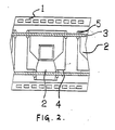
- Figure 2 is a plan view showing another embodiment of a tape assembly according to the present invention.
- the embodiment of Example 2 as compared to that of Example 1 shown in Figure 1, is characterized in that adhesive FT 3 is employed at two spaced apart places.
- the remaining features of Example 2 are identical to those of Example 1.
- Figure 3 is a plan view showing another embodiment of a tape assembly according to the present invention.
- the embodiment of Figure 3, as compared to Example 1 and to Example 2, is characterized in that each slit hole 5 has a minute or other thin connector 6 across it in order to maintain each semiconductor apparatus 2 attached to the FPC tape 1, even after the semiconductor apparatus 2 has been cut from the FPC tape 1 at the external cut lines 4, and without using adhesive FT 3.
- the minute connectors 6 By not cutting the minute connectors 6 which extend across the slit holes 5 when cutting the semiconductor apparatuses 2 from the FPC tape 1 at the external cut lines 4, the same effect is obtained as With the adhesive FT 3 of Example 1 and Example 2. Moreover, the minute connectors 6 can be provided at any position on the outer periphery of the semiconductor apparatuses 2.
- Figures 4(a) through (h) are plan views showing various embodiments of parts of tape assemblies according to the present invention, the various plan views relating to the area shown at A in Figure 3 and showing various shapes which may be adopted for the slit holes 5 and various dispositions which may be employed for the minute connectors 6.
- Figure 4 (a) to (d) show cases where the slit hole 5 is oval, and (e) to (h) show cases where the slit hole 5 is rectangular. Also, Figure 4, (a) and (e), show cases where the minute connectors 6 are provided singly in the central part of the slit hole 5; (b) and (f) show cases where the minute connectors 6 are provided in duplicate; Figure 4, (c) and (g), show cases where the minute connectors 6 are provided in triplicate; and Figure 4, (d) and (h) show cases where the minute connectors 6 slant sideways in the slit holes 5.
- the sizes of the slit holes 5 were from 0.3 mm to about 5.0 mm in width, and from 2.0 mm to about 10 mm in length. Moreover, the widths of the minute connectors 6 were from 0.1 mm to about 1.0 mm.
- Figure 5 is a drawing illustrating one embodiment of a method according to the present invention for using the said tape assembly.
- one part of the semiconductor apparatus 2 is attached to the FPC tape 1 with adhesive FT 3, but another part thereof has already been cut out from the FPC tape 1 at the external cut line 4.
- the semiconductor apparatus 2 can be separated from the FPC tape 1 by cutting the adhesive FT 3.
- the steps for carrying this out are shown in Figure 6(a) to (d), these views being along section C-C in Figure 5.
- the adhesive FT 3 is attached to the FPC tape 1.
- a cutter 7 is shown as standing by directly over the semiconductor apparatus 2 and a slit hole 5 of the FPC tape 1, in Figure 6(b), the cutter 7 is shown as having dropped down to a position where it may or may not contact the adhesive FT 3. In this state, heating of the cutter 7 is effected by passing electric current through the cutter 7.
- the heated cutter 7 is shown as having dropped further so that it cuts the adhesive FT 3 by melting it.
- the cutter 7 is shown as having dropped still further so that it cuts the adhesive FT 3 completely. In this manner, the semiconductor apparatus 2 is cut off from the FPC tape 1 by advancing from the state shown in Figure 6(a) to the state shown in (d).
- Figure 7 is a drawing illustrating another embodiment of a method according to the present invention for assembling a tape assembly.
- the semiconductor apparatus 2 can be separated from the FPC tape 1 by cutting the minute connectors 6 just before the semiconductor apparatus 2 is provided with outer lead bonding at the OLB terminal of the OLB element.
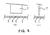
- Figure 8(a) is a sectional view along D-D of Figure 7.
- the cutter 7 is shown as standing by directly over a slit hole 5 of the semiconductor apparatus 2 and the FPC tape 1.
- the cutter 7 falls in the same manner as in Example 5, the minute connectors 6 are cut, and the semiconductor apparatus 2 is cut off from the FPC tape 1.
- the semiconductor apparatuses 2 can be transported in the taped state and in roll form until just before OLB.
- a sharp cutter made of stainless steel was used as the cutter 7 in the present example.
- FIG. 9 illustrates a method of inner lead bonding (hereafter called ILB) which may be carried out prior to the OLB described above.
- ILB inner lead bonding
- a wiring circuit part 2-1 of the semiconductor apparatus 2 is placed on the FPC tape 1, and the FPC tape 1 is wound on a reel 12-1.
- the FPC tape 1 is drawn from the reel 12-1 and, in the region (a), a semiconductor element 2-2 of the semiconductor apparatus 2 is attached under hot compression by a bonding tool 8 to the wiring circuit part 2-1 of the semiconductor apparatus 2 on the FPC tape 1, and is connected electrically and mechanically by a gang bonding method.
- the semiconductor apparatus 2 on the FPC tape 1 is painted with adhesive 11 ejected from a nozzle 9. Further, the painting of the adhesive 11 may be effected by a method such as printing.
- the semiconductor apparatus 2 on the FPC tape 1 is given, in the region (c), an electrical inspection by placing probes 10 of an inspection device 16 in contact with terminals of the semiconductor apparatus 2. After this, the FPC tape 1 is wound up again onto a reel 12-2. In this way, it is possible to process the semiconductor apparatuses 2 continuously in one pass and in the taped state during an ILB process which precedes the OLB process described above.
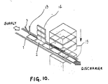
- FIG 10 is a schematic drawing that shows the adhesive FT 3 attached to the FPC tape 1 up to the external cut of the semiconductor apparatus 2.
- the adhesive FT 3 on the FPC tape 1 is temporarily held by an FT temporary press tool 13, after which it is pressed and adhered to the FPC tape 1 by an hot press adhesion device 14.
- each semiconductor apparatus 2 on the FPC tape 1 is cut by an external cut device 15 along the external cut lines 4, leaving part of each semiconductor apparatus 2 fastened to the FPC tape 1 by the adhesive FT 3. Consequently, each semiconductor apparatus 2 is held fastened in this state to the FPC tape 1 only by the adhesive FT 3.
- the supply and discharge of the FPC tape 1 and thus of the semiconductor apparatus 2 were both done in reel form.
- ACF was used as the adhesive FT 3 and the operating conditions of the hot press adhesion device 14 were a temperature of 120°C, a pressure of 10 kg/cm2, and a time of 3 seconds. Also, the pressing pressure exerted by the external cut device 15 was 4 kg/cm2.
- Figure 11 illustrates a method in which the adhesive FT3 is cut by the time that the semiconductor apparatus is connected to the terminal part of a liquid crystal display element 17, for example.
- a plurality of semiconductor apparatuses 2-3 each of which has one part held fastened to FPC tape 1 by adhesive FT 3, after being transported to a prescribed position by the movement of FPC tape 1, has the adhesive FT 3 cut by cutters 7, and is completely separated from the FPC tape 1 for the first time.
- Semiconductor apparatus 2-4 now constituted by a separated single solid-state element, is transported to the vicinity of the terminal part of liquid crystal display element 17 by a transport means (not shown). Then it is positioned by a positioning means 2-5, that is, by optical recognition of the terminal part of the semiconductor apparatus 2-4 and the terminal part of the liquid crystal display element 17.
- preliminary press adhesion is effected by means of a press adhesion head 16, and the semiconductor apparatus 2-6 is attached to the terminal part of the liquid crystal display element 17.
- the operating conditions of the press adhesion head 16 were room temperature, a pressure of 3 kg/cm2, and a time of 1 second.
- FIG 12 is a front view of an apparatus for carrying out the method illustrated in Figure 11.
- the FPC tape 1 after the completion of the method illustrated in Figure 10, is shown as having been wound on a reel 12.
- each semiconductor apparatus 2 which is fastened to the FPC tape 1 by adhesive FT 3 has the latter cut at the region A so that it is separated from the FPC tape 1, and is mounted on the terminal part of the liquid crystal display element.
- the FPC tape 1 which has thus been separated from the semiconductor apparatuses 2 is cut at an FPC tape cutter 18 and is removed.
Landscapes
- Engineering & Computer Science (AREA)
- Manufacturing & Machinery (AREA)
- Microelectronics & Electronic Packaging (AREA)
- Wire Bonding (AREA)
- Supply And Installment Of Electrical Components (AREA)
Applications Claiming Priority (2)
| Application Number | Priority Date | Filing Date | Title |
|---|---|---|---|
| JP1221228A JP2751450B2 (ja) | 1989-08-28 | 1989-08-28 | テープキャリアの実装構造及びその実装方法 |
| JP221228/89 | 1989-08-28 |
Publications (1)
| Publication Number | Publication Date |
|---|---|
| EP0415663A1 true EP0415663A1 (fr) | 1991-03-06 |
Family
ID=16763478
Family Applications (1)
| Application Number | Title | Priority Date | Filing Date |
|---|---|---|---|
| EP90309302A Withdrawn EP0415663A1 (fr) | 1989-08-28 | 1990-08-24 | Assemblage avec bande |
Country Status (4)
| Country | Link |
|---|---|
| US (3) | US5177596A (fr) |
| EP (1) | EP0415663A1 (fr) |
| JP (1) | JP2751450B2 (fr) |
| KR (1) | KR910005416A (fr) |
Cited By (3)
| Publication number | Priority date | Publication date | Assignee | Title |
|---|---|---|---|---|
| WO1993005636A1 (fr) * | 1991-09-02 | 1993-03-18 | Siemens Nixdorf Informationssysteme Aktiengesellschaft | Support auxiliaire en forme de bande servant d'aide pour le montage ligne par ligne de puces a semiconducteur sur la surface de contact d'un element porteur |
| EP1313357A4 (fr) * | 2001-03-26 | 2005-04-06 | Ibiden Co Ltd | Substrat a elements multiples et son procede de production |
| EP1429386A3 (fr) * | 2002-12-09 | 2005-04-13 | Nitto Denko Corporation | Bande de support pour TAB et procédé de fabrication |
Families Citing this family (33)
| Publication number | Priority date | Publication date | Assignee | Title |
|---|---|---|---|---|
| JP3178181B2 (ja) * | 1993-09-06 | 2001-06-18 | 松下電器産業株式会社 | アウターリードボンディング装置およびアウターリードボンディング方法 |
| JP3189531B2 (ja) * | 1993-10-01 | 2001-07-16 | 松下電器産業株式会社 | 平板電極ユニットおよびその製造方法 |
| DE4404986B4 (de) * | 1994-02-17 | 2008-08-21 | Robert Bosch Gmbh | Einrichtung zur Kontaktierung elektrischer Leiter sowie Verfahren zur Herstellung einer derartigen Einrichtung |
| CN1217869A (zh) * | 1996-05-10 | 1999-05-26 | 松下电器产业株式会社 | 零件装配方法及零件装配装置 |
| US6687969B1 (en) | 1997-05-16 | 2004-02-10 | Micron Technology, Inc. | Methods of fixturing flexible substrates and methods of processing flexible substrates |
| US5972152A (en) | 1997-05-16 | 1999-10-26 | Micron Communications, Inc. | Methods of fixturing flexible circuit substrates and a processing carrier, processing a flexible circuit and processing a flexible circuit substrate relative to a processing carrier |
| JP3482850B2 (ja) * | 1997-12-08 | 2004-01-06 | セイコーエプソン株式会社 | 半導体装置及びその製造方法、回路基板並びに電子機器 |
| JP3873478B2 (ja) * | 1997-12-25 | 2007-01-24 | セイコーエプソン株式会社 | 液晶表示装置、電子機器及び液晶表示装置の製造方法 |
| US6057174A (en) * | 1998-01-07 | 2000-05-02 | Seiko Epson Corporation | Semiconductor device, method of fabricating the same, and electronic apparatus |
| WO1999041782A2 (fr) * | 1998-02-17 | 1999-08-19 | Koninklijke Philips Electronics N.V. | Bande a modules presentant des modules supports de donnees a double-mode de liaison |
| JP3536728B2 (ja) | 1998-07-31 | 2004-06-14 | セイコーエプソン株式会社 | 半導体装置及びテープキャリア並びにそれらの製造方法、回路基板、電子機器並びにテープキャリア製造装置 |
| JP3512655B2 (ja) * | 1998-12-01 | 2004-03-31 | シャープ株式会社 | 半導体装置およびその製造方法並びに該半導体装置の製造に使用される補強用テープ |
| US7169643B1 (en) * | 1998-12-28 | 2007-01-30 | Seiko Epson Corporation | Semiconductor device, method of fabricating the same, circuit board, and electronic apparatus |
| JP3558921B2 (ja) * | 1999-05-14 | 2004-08-25 | シャープ株式会社 | テープキャリア並びにテープキャリア型半導体装置の製造方法 |
| DE10014620A1 (de) * | 2000-03-24 | 2001-09-27 | Andreas Plettner | Verfahren zur Herstellung eines Trägerbandes mit einer Vielzahl von elektrischen Einheiten, jeweils aufweisend einen Chip und Kontaktelemente |
| US6719188B2 (en) * | 2001-07-24 | 2004-04-13 | International Business Machines Corporation | Rework methods for lead BGA/CGA |
| JP3825664B2 (ja) | 2001-09-27 | 2006-09-27 | 株式会社東芝 | フィルム基板、フィルム基板の製造方法及びフィルム基板付回路基板の製造方法 |
| JP3726961B2 (ja) * | 2002-06-26 | 2005-12-14 | 三井金属鉱業株式会社 | Cofフィルムキャリアテープ及びその製造方法 |
| US7371970B2 (en) * | 2002-12-06 | 2008-05-13 | Flammer Jeffrey D | Rigid-flex circuit board system |
| EP1605739A4 (fr) * | 2003-04-18 | 2009-08-19 | Ibiden Co Ltd | Tableau de connexions rigide-flexible |
| JP2005107438A (ja) * | 2003-10-02 | 2005-04-21 | Matsushita Electric Ind Co Ltd | プラズマディスプレイ装置用半導体装置の製造方法 |
| JP3829939B2 (ja) * | 2003-11-14 | 2006-10-04 | セイコーエプソン株式会社 | 半導体装置の製造方法及び製造装置 |
| KR101002346B1 (ko) * | 2003-12-30 | 2010-12-20 | 엘지디스플레이 주식회사 | 칩 실장형 필름 패키지 |
| JP4536430B2 (ja) * | 2004-06-10 | 2010-09-01 | イビデン株式会社 | フレックスリジッド配線板 |
| TWI266574B (en) * | 2004-09-13 | 2006-11-11 | Advanced Semiconductor Eng | Circuit substrate |
| WO2006044739A2 (fr) * | 2004-10-18 | 2006-04-27 | Intraglobal Corporation | Module microelectronique et procede associe |
| KR100684793B1 (ko) | 2004-12-07 | 2007-02-20 | 삼성에스디아이 주식회사 | 릴상의 테이프 캐리어 패키지와 이를 적용한 플라즈마디스플레이 장치 |
| KR100793068B1 (ko) * | 2005-03-07 | 2008-01-10 | 엘지전자 주식회사 | 더미 패턴을 이용한 티씨피 제조 방법 및 그 더미 패턴 필름 |
| DE102007041921A1 (de) * | 2007-09-04 | 2009-03-05 | Siemens Ag | Verfahren zur Herstellung und Kontaktierung von elektronischen Bauelementen mittels einer Substratplatte, insbesondere DCB-Keramik-Substratplatte |
| CN102057763B (zh) * | 2008-06-10 | 2016-01-20 | 皇家飞利浦电子股份有限公司 | 电子纺织品、制造其的方法以及用于其的纱线 |
| GB2502305B (en) * | 2012-05-22 | 2015-07-29 | Plastic Logic Ltd | Electronic reading devices |
| PL3957459T3 (pl) | 2013-09-27 | 2025-11-03 | Tactotek Oy | Sposób wytwarzania struktury elektromechanicznej i układ do realizacji tego sposobu |
| CN116403949B (zh) * | 2023-06-08 | 2023-08-15 | 深圳市磐锋精密技术有限公司 | 一种全自动cof邦定机智能传动控制系统及方法 |
Citations (7)
| Publication number | Priority date | Publication date | Assignee | Title |
|---|---|---|---|---|
| EP0059092A1 (fr) * | 1981-02-23 | 1982-09-01 | Thomas Louis Angelucci | Bande de support pour conducteurs à circuit imprimé |
| US4413308A (en) * | 1981-08-31 | 1983-11-01 | Bell Telephone Laboratories, Incorporated | Printed wiring board construction |
| GB2137805A (en) * | 1982-11-19 | 1984-10-10 | Stanley Bracey | Chip Carrier |
| GB2164794A (en) * | 1984-09-17 | 1986-03-26 | Lohja Ab Oy | Method for encapsulating semiconductor components mounted on a carrier tape |
| US4681654A (en) * | 1986-05-21 | 1987-07-21 | International Business Machines Corporation | Flexible film semiconductor chip carrier |
| WO1988006348A1 (fr) * | 1987-02-20 | 1988-08-25 | Lsi Logic Corporation | Boitier de circuits integres |
| EP0324244A2 (fr) * | 1988-01-15 | 1989-07-19 | International Business Machines Corporation | Empaquetage à transport automatique sur bande pour une puce semi-conductrice comprenant du découplage |
Family Cites Families (35)
| Publication number | Priority date | Publication date | Assignee | Title |
|---|---|---|---|---|
| US2596068A (en) * | 1946-10-10 | 1952-05-06 | Wilson Jones Co | Casemaker |
| US2556787A (en) * | 1949-02-12 | 1951-06-12 | Florez Company Inc De | Register control for web fed casemaking machines |
| US3118804A (en) * | 1957-05-06 | 1964-01-21 | Wood Products Dev Company Inc | Apparatus for making parquet flooring blocks |
| US3488840A (en) * | 1963-12-27 | 1970-01-13 | Ibm | Method of connecting microminiaturized devices to circuit panels |
| US3376185A (en) * | 1964-08-12 | 1968-04-02 | Balsa Dev Corp | Contour core structure |
| US3440027A (en) * | 1966-06-22 | 1969-04-22 | Frances Hugle | Automated packaging of semiconductors |
| US3499218A (en) * | 1966-10-31 | 1970-03-10 | Electro Mechanisms Inc | Multilayer circuit boards and methods of making the same |
| US3689991A (en) * | 1968-03-01 | 1972-09-12 | Gen Electric | A method of manufacturing a semiconductor device utilizing a flexible carrier |
| US3772108A (en) * | 1970-12-21 | 1973-11-13 | I Lezhen | Method of producing fur products and a device for carrying out the method |
| US3968563A (en) * | 1975-03-27 | 1976-07-13 | E. I. Du Pont De Nemours And Company | Precision registration system for leads |
| US4063993A (en) * | 1975-07-07 | 1977-12-20 | National Semiconductor Corporation | Method of making gang bonding interconnect tape for semiconductive devices |
| US4222516A (en) * | 1975-12-31 | 1980-09-16 | Compagnie Internationale Pour L'informatique Cii-Honeywell Bull | Standardized information card |
| US4282056A (en) * | 1979-01-04 | 1981-08-04 | Tokujiro Okui | Both-surface adhesive tape producing apparatus |
| US4251852A (en) * | 1979-06-18 | 1981-02-17 | International Business Machines Corporation | Integrated circuit package |
| US4364785A (en) * | 1979-10-11 | 1982-12-21 | Michel Wajs | Association of a piece of fabric with a sheet of PVC |
| US4284454A (en) * | 1980-05-12 | 1981-08-18 | Joa Curt G | Method and apparatus for applying elastic bands transversely to a diaper line |
| US4377316A (en) * | 1981-02-27 | 1983-03-22 | International Business Machines Corporation | High density interconnection means for chip carriers |
| US4426768A (en) * | 1981-12-28 | 1984-01-24 | United Technologies Corporation | Ultra-thin microelectronic pressure sensors |
| US4549200A (en) * | 1982-07-08 | 1985-10-22 | International Business Machines Corporation | Repairable multi-level overlay system for semiconductor device |
| US4664736A (en) * | 1983-01-24 | 1987-05-12 | Faasse Jr Adrain L | Pharmaceutical packaging method |
| US4606962A (en) * | 1983-06-13 | 1986-08-19 | Minnesota Mining And Manufacturing Company | Electrically and thermally conductive adhesive transfer tape |
| US4685998A (en) * | 1984-03-22 | 1987-08-11 | Thomson Components - Mostek Corp. | Process of forming integrated circuits with contact pads in a standard array |
| JPS60239043A (ja) * | 1984-05-14 | 1985-11-27 | Oki Electric Ind Co Ltd | 半導体装置用パツケ−ジの製造方法 |
| US4581479A (en) * | 1984-11-16 | 1986-04-08 | Moore Theodore W | Dimensionally precise electronic component mount |
| IT1213259B (it) * | 1984-12-18 | 1989-12-14 | Sgs Thomson Microelectronics | Gruppo a telaio di conduttori per circuiti integrati con capacita' di termodispersione incrementata, erelativo procedimento. |
| US4870476A (en) * | 1986-02-13 | 1989-09-26 | Vtc Incorporated | Integrated circuit packaging process and structure |
| US4820658A (en) * | 1986-04-14 | 1989-04-11 | Gte Products Corporation | Method of making a packaged IC chip |
| US4721992A (en) * | 1986-06-26 | 1988-01-26 | National Semiconductor Corporation | Hinge tape |
| US4835120A (en) * | 1987-01-12 | 1989-05-30 | Debendra Mallik | Method of making a multilayer molded plastic IC package |
| FR2616995A1 (fr) * | 1987-06-22 | 1988-12-23 | Ebauchesfabrik Eta Ag | Procede de fabrication de modules electroniques |
| FR2622353B1 (fr) * | 1987-10-22 | 1990-03-23 | Bendix Electronics Sa | Produit en bande pour supporter et convoyer des composants electroniques et procede pour sa fabrication |
| US4987475A (en) * | 1988-02-29 | 1991-01-22 | Digital Equipment Corporation | Alignment of leads for ceramic integrated circuit packages |
| US5034591A (en) * | 1988-03-22 | 1991-07-23 | Amdahl Corporation | Tape automated bonding leads having a stiffener and a method of bonding with same |
| US4842662A (en) * | 1988-06-01 | 1989-06-27 | Hewlett-Packard Company | Process for bonding integrated circuit components |
| US4981817A (en) * | 1988-12-29 | 1991-01-01 | International Business Machines Corporation | Tab method for implementing dynamic chip burn-in |
-
1989
- 1989-08-28 JP JP1221228A patent/JP2751450B2/ja not_active Expired - Fee Related
-
1990
- 1990-08-24 EP EP90309302A patent/EP0415663A1/fr not_active Withdrawn
- 1990-08-27 KR KR1019900013211A patent/KR910005416A/ko not_active Withdrawn
- 1990-08-28 US US07/573,885 patent/US5177596A/en not_active Expired - Lifetime
-
1993
- 1993-10-13 US US08/136,478 patent/US5389191A/en not_active Expired - Lifetime
- 1993-10-19 US US08/139,629 patent/US5427641A/en not_active Expired - Lifetime
Patent Citations (7)
| Publication number | Priority date | Publication date | Assignee | Title |
|---|---|---|---|---|
| EP0059092A1 (fr) * | 1981-02-23 | 1982-09-01 | Thomas Louis Angelucci | Bande de support pour conducteurs à circuit imprimé |
| US4413308A (en) * | 1981-08-31 | 1983-11-01 | Bell Telephone Laboratories, Incorporated | Printed wiring board construction |
| GB2137805A (en) * | 1982-11-19 | 1984-10-10 | Stanley Bracey | Chip Carrier |
| GB2164794A (en) * | 1984-09-17 | 1986-03-26 | Lohja Ab Oy | Method for encapsulating semiconductor components mounted on a carrier tape |
| US4681654A (en) * | 1986-05-21 | 1987-07-21 | International Business Machines Corporation | Flexible film semiconductor chip carrier |
| WO1988006348A1 (fr) * | 1987-02-20 | 1988-08-25 | Lsi Logic Corporation | Boitier de circuits integres |
| EP0324244A2 (fr) * | 1988-01-15 | 1989-07-19 | International Business Machines Corporation | Empaquetage à transport automatique sur bande pour une puce semi-conductrice comprenant du découplage |
Cited By (4)
| Publication number | Priority date | Publication date | Assignee | Title |
|---|---|---|---|---|
| WO1993005636A1 (fr) * | 1991-09-02 | 1993-03-18 | Siemens Nixdorf Informationssysteme Aktiengesellschaft | Support auxiliaire en forme de bande servant d'aide pour le montage ligne par ligne de puces a semiconducteur sur la surface de contact d'un element porteur |
| EP1313357A4 (fr) * | 2001-03-26 | 2005-04-06 | Ibiden Co Ltd | Substrat a elements multiples et son procede de production |
| CN101980590B (zh) * | 2001-03-26 | 2012-06-06 | 揖斐电株式会社 | 多片基板及其制造方法 |
| EP1429386A3 (fr) * | 2002-12-09 | 2005-04-13 | Nitto Denko Corporation | Bande de support pour TAB et procédé de fabrication |
Also Published As
| Publication number | Publication date |
|---|---|
| JPH0384955A (ja) | 1991-04-10 |
| JP2751450B2 (ja) | 1998-05-18 |
| KR910005416A (ko) | 1991-03-30 |
| US5427641A (en) | 1995-06-27 |
| US5389191A (en) | 1995-02-14 |
| US5177596A (en) | 1993-01-05 |
Similar Documents
| Publication | Publication Date | Title |
|---|---|---|
| US5427641A (en) | Method of forming a mounting structure on a tape carrier | |
| JP3512655B2 (ja) | 半導体装置およびその製造方法並びに該半導体装置の製造に使用される補強用テープ | |
| JP3536728B2 (ja) | 半導体装置及びテープキャリア並びにそれらの製造方法、回路基板、電子機器並びにテープキャリア製造装置 | |
| US20080096318A1 (en) | Method of connecting carrier tapes and tcp mounting apparatus used therefor | |
| US4044460A (en) | Method of mounting prefabricated contacts for printed circuit card connectors | |
| US6066231A (en) | Laminating device for joining a metal strip and an insulating material strip | |
| JP3509573B2 (ja) | フレキシブル基板用テープ材、フレキシブル基板の製造方法、半導体装置の製造方法及び液晶装置の製造方法 | |
| JP4151083B2 (ja) | 異方導電性接着テープの貼付け方法および装置 | |
| JP4116509B2 (ja) | テープ部材の貼着装置 | |
| JP2769263B2 (ja) | 転写用異方性接着剤テープの作成方法および装置 | |
| JPH07161771A (ja) | フィルムキャリア、電子部品および離型紙剥離方法 | |
| JP2007057957A (ja) | Acf貼り付け方法及びacf貼り付け装置 | |
| JP2003066479A (ja) | 液晶パネルへのtab部品の圧着方法 | |
| JPH1022035A (ja) | コネクタターミナルの実装方法及び実装方法に用いるコネクタターミナルユニット | |
| KR100780172B1 (ko) | 탭용 테이프 캐리어 | |
| CN115250579B (zh) | 压力感应模组的制作方法及压力感应模组 | |
| JP2637369B2 (ja) | 電子部品のテーピング方法 | |
| US6612475B2 (en) | Tape shifting means | |
| JPH06164115A (ja) | 異方導電性接着剤の転写方法 | |
| JP2003137474A (ja) | 両面粘着性テープの切断・貼着装置 | |
| KR100643428B1 (ko) | 전자 패키징 필름의 본딩장치 | |
| JPH04162440A (ja) | テープキャリア、テープキャリアの製造方法及びテープキャリアの実装方法 | |
| JP2637370B2 (ja) | 電子部品のテーピング方法 | |
| JP4031661B2 (ja) | 接続部材貼付装置 | |
| JPH10261896A (ja) | 金属端子片のテーピング装置、金属端子片のテーピング方法、このテーピング装置またはテーピング方法によりテーピングされた金属端子片、およびこの金属端子片の実装方法 |
Legal Events
| Date | Code | Title | Description |
|---|---|---|---|
| PUAI | Public reference made under article 153(3) epc to a published international application that has entered the european phase |
Free format text: ORIGINAL CODE: 0009012 |
|
| AK | Designated contracting states |
Kind code of ref document: A1 Designated state(s): DE GB NL |
|
| 17P | Request for examination filed |
Effective date: 19910813 |
|
| STAA | Information on the status of an ep patent application or granted ep patent |
Free format text: STATUS: THE APPLICATION HAS BEEN WITHDRAWN |
|
| 18W | Application withdrawn |
Withdrawal date: 19920129 |