EP0415725B1 - Appareil d'enregistrement d'images - Google Patents
Appareil d'enregistrement d'images Download PDFInfo
- Publication number
- EP0415725B1 EP0415725B1 EP90309416A EP90309416A EP0415725B1 EP 0415725 B1 EP0415725 B1 EP 0415725B1 EP 90309416 A EP90309416 A EP 90309416A EP 90309416 A EP90309416 A EP 90309416A EP 0415725 B1 EP0415725 B1 EP 0415725B1
- Authority
- EP
- European Patent Office
- Prior art keywords
- image
- clock
- output
- signal
- resolution
- Prior art date
- Legal status (The legal status is an assumption and is not a legal conclusion. Google has not performed a legal analysis and makes no representation as to the accuracy of the status listed.)
- Expired - Lifetime
Links
Images


Classifications
-
- H—ELECTRICITY
- H04—ELECTRIC COMMUNICATION TECHNIQUE
- H04N—PICTORIAL COMMUNICATION, e.g. TELEVISION
- H04N1/00—Scanning, transmission or reproduction of documents or the like, e.g. facsimile transmission; Details thereof
- H04N1/40—Picture signal circuits
- H04N1/40025—Circuits exciting or modulating particular heads for reproducing continuous tone value scales
- H04N1/4005—Circuits exciting or modulating particular heads for reproducing continuous tone value scales with regulating circuits, e.g. dependent upon ambient temperature or feedback control
-
- G—PHYSICS
- G06—COMPUTING OR CALCULATING; COUNTING
- G06K—GRAPHICAL DATA READING; PRESENTATION OF DATA; RECORD CARRIERS; HANDLING RECORD CARRIERS
- G06K15/00—Arrangements for producing a permanent visual presentation of the output data, e.g. computer output printers
- G06K15/02—Arrangements for producing a permanent visual presentation of the output data, e.g. computer output printers using printers
- G06K15/12—Arrangements for producing a permanent visual presentation of the output data, e.g. computer output printers using printers by photographic printing, e.g. by laser printers
-
- H—ELECTRICITY
- H04—ELECTRIC COMMUNICATION TECHNIQUE
- H04N—PICTORIAL COMMUNICATION, e.g. TELEVISION
- H04N1/00—Scanning, transmission or reproduction of documents or the like, e.g. facsimile transmission; Details thereof
- H04N1/04—Scanning arrangements, i.e. arrangements for the displacement of active reading or reproducing elements relative to the original or reproducing medium, or vice versa
- H04N1/0402—Scanning different formats; Scanning with different densities of dots per unit length, e.g. different numbers of dots per inch (dpi); Conversion of scanning standards
- H04N1/0408—Different densities of dots per unit length
- H04N1/0411—Different densities of dots per unit length in the main scanning direction
-
- H—ELECTRICITY
- H04—ELECTRIC COMMUNICATION TECHNIQUE
- H04N—PICTORIAL COMMUNICATION, e.g. TELEVISION
- H04N1/00—Scanning, transmission or reproduction of documents or the like, e.g. facsimile transmission; Details thereof
- H04N1/04—Scanning arrangements, i.e. arrangements for the displacement of active reading or reproducing elements relative to the original or reproducing medium, or vice versa
- H04N1/0402—Scanning different formats; Scanning with different densities of dots per unit length, e.g. different numbers of dots per inch (dpi); Conversion of scanning standards
- H04N1/042—Details of the method used
- H04N1/0446—Varying the modulation time or intensity
-
- H—ELECTRICITY
- H04—ELECTRIC COMMUNICATION TECHNIQUE
- H04N—PICTORIAL COMMUNICATION, e.g. TELEVISION
- H04N1/00—Scanning, transmission or reproduction of documents or the like, e.g. facsimile transmission; Details thereof
- H04N1/40—Picture signal circuits
- H04N1/40025—Circuits exciting or modulating particular heads for reproducing continuous tone value scales
- H04N1/40037—Circuits exciting or modulating particular heads for reproducing continuous tone value scales the reproducing element being a laser
Definitions
- the present invention relates to an image recording apparatus capable of changing over a recording resolution.
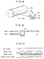
- Fig. 8 is a perspective view for explaining an image forming theory in a conventional image printing apparatus.
- This apparatus includes a photosensitive drum 100 serving as an electrostatic latent image carrier which is rotated at a constant speed in a direction indicated by an arrow.
- a semiconductor laser 101 outputs a laser beam 105 which is ON/OFF-modulated on the basis of print information input from a host computer (not shown) or the like.
- a polygonal mirror 102 is rotated by a scanner motor 103 at a predetermined speed to deflect the laser beam 105 incident through an optical system such as a collimator lens.
- a latent image is formed on the photosensitive drum 100 through a focusing lens 106 having f- ⁇ characteristics.
- a beam detector 104 receives the laser beam 105 scanned on the photosensitive drum 100 from the left to the right prior to scanning of an image write area and outputs a beam detection signal to a controller (not shown) to generate a horizontal sync signal BD which defines a write start position in the main scanning direction.
- the laser beam 105 modulated on the basis of image information is incident from the laser 101 to the photosensitive drum 100 serving as a latent image carrier through the rotating polygonal mirror 102.
- the laser beam 105 is scanned on the photosensitive drum 100 to form a latent image.
- the latent image is visualized into a toner image by a developing unit (not shown).
- the toner image is transferred to and fixed on a recording sheet, thereby forming an image.
- Fig. 9 is a control block diagram for explaining a control arrangement of the image printing apparatus shown in Fig. 8.
- a printer controller 200 develops image information received from a host computer or the like into a bit map in an internal memory. Image data 206 and an image clock 207 for latching this image data are output to a printer engine image control circuit 204 in synchronism with the BD signal 212 obtained from a printer engine BD signal detector 213. At the same time, the printer controller 200 performs serial communication with a print engine print control circuit 201 through a serial communication bus 205.
- a scanner driver 202 controls a scanner motor 103 shown in Fig. 8 and rotates it to a predetermined speed on the basis of a motor control signal 208 output from the print control circuit 201.
- a laser driver 203 controls emission of a laser beam from the semiconductor laser 101 (Fig. 8) on the basis of a laser control signal 209 output from the print control circuit 201.
- the image control circuit 204 receives image data 206 output in synchronism with the image clock 207 from the printer controller 200 and outputs a laser drive signal 211 to the laser driver 203.
- the image control circuit 204 receives an image control signal 210 from the print control circuit 201 and performs signal processing associated with resolution change-over.
- Fig. 10 is a block diagram of an arrangement of the image control circuit 204 (Fig. 9) which is exemplified by a D flip-flop DFF.
- Fig. 11 is a timing chart for explaining operations of the respective parts in Fig. 9, and the same reference numerals as in Fig. 9 denote the same parts in Fig. 11.
- the BD signal detector 213 shown in Fig. 9 When the beam detector 104 shown in Fig. 8 receives the laser beam 105, the BD signal detector 213 shown in Fig. 9 outputs the BD signal 212 to the printer controller 200.
- the image data 206 is output to the image control circuit 204 in synchronism with the image clock 207.
- the printer controller 200 serially transmits control information (e.g., a resolution change-over signal) to the print control circuit 201.
- the print control circuit 201 performs change-over processing such as speed change-over of the scanner driver 202. Therefore, an image can be printed at different resolutions in a single printing processor.
- Japan JP - A - 62 280 040 discloses an image recording apparatus using a laser beam which laser lighting time is controlled by a circuit in order to obtain different resolving powers per picture elements.
- the document DE - A - 3 738 469 discloses general background art: an image recording apparatus which uses a laser beam with two scanning directions which is modulated with respect to the image signal. The thickness of a pixel is determined by the intensity of the beam.
- Fig. 1 is a block diagram showing an arrangement of an image printing apparatus according to an embodiment of the present invention.
- the image printing apparatus comprises a printer controller 1 having a bit map memory for developing image information from a host computer into video information which is then sent to a printer engine.
- the printer controller 1 serially sends to print control circuit 2 print control information (e.g., a resolution change-over request) corresponding to bit information developed in the bit map memory.
- print control circuit 2 print control information (e.g., a resolution change-over request) corresponding to bit information developed in the bit map memory.
- the printer controller 1 In synchronism with a BD signal 14 sent from a BD signal detection circuit 5, the printer controller 1 also outputs to an image control circuit 6 an image clock 13 having one period corresponding to one pixel of an image and image data 12 output at a trailing edge of the image clock 13.
- the print control circuit 2 performs serial communication with the printer controller 1 and signals a state of the printer engine to the printer controller 1 and controls the printer engine state in response to a request such as a resolution change-over request from the printer controller 1.
- a resolution setting means 2a sets and changes over a frequency of the image clock 13 and a scanning speed of an optical scanning system in accordance with resolution information 10 corresponding to the image information (in this embodiment, a motor control signal 8 for changing a preset speed control constant of a scanner driver 3 is sent to the scanner driver 3).
- the resolution setting means 2a controls a scanner speed corresponding to the resolution. Note that the speed is increased as the resolution is increased.
- the print control circuit 2 sends the resolution information 10 to the image control circuit 6 which generates a laser drive signal 15.
- a duty ratio setting means 6a in the image control circuit 6 controls a signal duty ratio of one period of the image clock 13 for a laser ON period to be a value corresponding to the resolution.
- a light beam having an optimal light amount corresponding to the resolution is incident on the image carrier in units of pixels.
- a laser driver 4 causes to radiate on a photosensitive drum 100 a laser beam 105 ON/OFF-modulated by a laser control signal 9 and the laser drive signal 15 from the print control circuit 2.
- the image control circuit 6 receives an image control signal 11 output from the print control circuit 2 and performs signal processing associated with resolution change-over and change-over operations of the image clock 13.
- the printer controller 1 is connected to the print control circuit 2 through a serial communication bus 7.
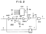
- Fig. 2 is a circuit diagram for explaining an operation of the image control circuit 6 shown in Fig. 1.
- the same reference numerals as in Fig. 1 denote the same parts in Fig. 2.
- An 8-bit data bus consists of bit lines D0 to D7.
- the data bus outputs the resolution information 10 to a D/A converter COV.
- the D/A converter COV outputs a threshold voltage b for determining the signal duty ratio to one input terminal of comparator CMP.
- the image control circuit 6 also includes an gate circuit AND, a flip-flop FF1, resistors R1 to R5, capacitors C1 and C2, and amplifiers AMP1 and AMP2.
- the resistors R1 to R3, the amplifiers AMP1 and AMP2, and the like constitute a triangular wave generator ANG.
- a triangular wave c shown in Fig. 3 is input to the other input terminal of the comparator CMP.
- the input image data 12 is output from a port e to the flip-flop FF1.
- the image clock 13 is input to a terminal CK of the flip-flop FF1, and a signal f is output from its terminal Q to the gate circuit AND.
- a gate output is output from a port g to the laser driver 4 as the laser drive signal 15.
- Fig. 3 is a timing chart for explaining the operation of the circuit arrangement of Fig. 2.
- the D/A converter COV When the resolution information 10 is signaled to the image control circuit 6 through the data bus (D0 to D7) shown in Fig. 2, the D/A converter COV outputs a triangular wave threshold voltage Vs for setting the signal duty ratio to the comparator CMP through a line b .
- the triangular wave (c) input to the comparator CMP is waveshaped by a threshold voltage (b) shown in Fig. 3, thereby obtaining the image clock 13(d) representing a signal duty corresponding to the resolution information 10.
- the image data 12(e) is latched by the flip-flop FF1 at a leading edge of the image clock 13(a) and is output from the terminal Q to the gate circuit AND.
- the gate circuit AND outputs the laser drive signal 15 from its port g to the laser driver 4.
- the laser drive signal 15 is obtained by ANDing the signal f and the image clock (signal at the port d ) having a signal duty ratio corresponding to the resolution information 10.
- the laser drive signal 15 based on the conventional signal f becomes the laser drive signal 15 output from the port g . It is therefore possible to turn on the laser within a shorter period of time by one period of the image clock 13.
- the image data 12 output from the printer controller 1 is serially processed line by line by the image control circuit 6.
- the present invention is applicable to an apparatus for parallelly performing read and write access of the image data 12 by arranging a plurality of line buffers 17 and 18.
- Fig. 4 is a block diagram of an image printing apparatus according to another embodiment of the present invention.
- the same reference numerals as in Fig. 1 denote the same parts in Fig. 4.
- a write control circuit 16 sets the line buffer 17 or 18 in a write state in response to a write control signal 20 output from a print control circuit 2.
- the line buffers 17 and 18 constitute a toggle circuit in which one line buffer is set in a read state while the other line buffer is set in a write state, and vice versa.
- a read control circuit 19 sets the either the line buffer 17 or 18 in a read state in response to a read control signal 21 output from the print control circuit 2.
- the read control circuit 19 changes over a signal duty ratio of one period of an image clock 13 on the basis of resolution information 22 output from the print control circuit 2.
- This image printing apparatus generates write data 23 and 24, read data 25 and 26, and a transfer clock 27.
- Fig. 5 is a block diagram showing a detailed arrangement of the read control circuit 19 shown in Fig. 4.
- the same reference numerals as in Fig. 4 denote the same parts in Fig. 5.
- the read control circuit 19 includes image clock Xn oscillators 31-1 to 31-N for generating clocks having frequencies corresponding to recording resolutions, i.e., generate clock signals having frequencies (n times of the frequency of the image clock 13; eight times in this embodiment) corresponding to the resolutions.
- the resolutions are 300 DPI, 400 DPI, and 600 DPI.
- a decoder 32 decodes resolution data having bits D0 to D2 designated by resolution information 10 and selects one of the oscillators 31-1 to 31-N.
- a read clock generator 33 receives a BD signal 14 through a BD signal generator 41, counts 8-time image clocks from the leading edge by a predetermined number (3 in the embodiment shown in Fig. 6), and starts to frequency-divide the clock, thereby obtaining an image clock 33a.
- An internal counter in a duty change-over clock generator 34 counts the selected 8-time image clocks by a complement of a 3-bit value, and is then reset to input a duty change-over clock 34a having a larger duty ratio of the image clock to a gate circuit 43.
- Shift registers 35 and 36 read out image data 12 stored in line buffers 17 and 18 in synchronism with a read clock from the clock generator 33.
- the readout image data is output to the gate circuit 43 through a gate circuit 42.
- a shift register 37 writes the image data 12 sent from a printer controller 1 in the line buffers 17 and 18 in synchronism with the transfer clock 27.
- a frequency divider 38 outputs a clock obtained by frequency-dividing the transfer lock 27 to the line buffers 17 and 18.
- a frequency divider 39 outputs a clock obtained by frequency-dividing the image clock 33a to the line buffers 17 and 18.
- a chip selector 40 controls read/write enable states of the line buffers 17 and 18.
- the BD signal generator 41 waveshapes the input BD signal 14 and outputs a horizontal sync signal to the respective parts.
- Fig. 6 is a timing chart for explaining an operation of the circuit arrangement shown in Fig. 5.
- the internal counter in the duty change-over clock generator 34 counts 8-time image clocks by a complement of a 3-bit value in accordance with the resolution data (D0 to D2) and is then reset to generate the duty change-over clock 34a.
- the duty change-over clock 34a is output to the gate circuit 43.
- the duty of the image clock 13 defined by one of the oscillators 31-1 to 31-N which is selected by the resolution is changed over, thereby obtaining the laser drive signal 15 based on the image data.
- the duty change-over clock 34a is generated by the read control circuit 19.
- the duty change-over clock may be generated by an internal clock circuit in a printer controller 1.
- Fig. 7 is a block diagram showing an arrangement of an image printing apparatus according to still another embodiment of the present invention.
- the same reference numerals as in Fig. 1 denote the same parts in Fig. 7.
- a duty change-over clock 50 is generated by an internal clock circuit in a printer controller 1 and is output to an image control circuit 6.
- the printer controller 1 analyzes image information input from a host computer and generates the duty change-over clock 50 corresponding to a desired resolution when the resolution change-over operation is required and is output to the image control circuit 6.
- image data 12 is output to the image control circuit 6 in synchronism with an image clock 13 and is ANDed with the duty change-over clock 50 to obtain laser drive signal 15.
- the laser drive signal 15 is output to a laser driver 4. Therefore, modifications of a conventional circuit can be minimized, and the laser drive signal 15 corresponding to the desired resolution can be generated and output at low cost.
- a resolution setting means for setting and changing over a frequency of an image clock signal and a scanning speed of an optical scanning system in accordance with resolution information designated by image information and a duty ratio setting means for changing over a signal duty ratio of the image clock signal having a predetermined frequency set by the resolution setting means in accordance with the designated resolution.
- a light beam ON time for one pixel can be optimally set without changing a beam spot size while the image clock is changed over in correspondence with the resolution.
- the image quality of a thin line image can be greatly improved as compared with an image based on the conventional image clock. Therefore, the line width of an image during formation of a vertical line image will not be increased, and thin lines such as a table image serving as a format image and rulers can be drawn, thus providing many practical advantages.
Landscapes
- Engineering & Computer Science (AREA)
- Multimedia (AREA)
- Signal Processing (AREA)
- Physics & Mathematics (AREA)
- Optics & Photonics (AREA)
- General Engineering & Computer Science (AREA)
- General Physics & Mathematics (AREA)
- Theoretical Computer Science (AREA)
- Laser Beam Printer (AREA)
- Fax Reproducing Arrangements (AREA)
- Mechanical Optical Scanning Systems (AREA)
- Dot-Matrix Printers And Others (AREA)
Claims (5)
- Appareil d'enregistrement d'images destiné à enregistrer une image à différentes définitions, comportant :des premiers moyens de sortie (1) destinés à délivrer en sortie des données d'images (12, e) ;des seconds moyens de sortie (1, 33) destinés à générer un signal d'horloge (13, a, 33a) dont la période correspond à la largeur d'un pixel d'une image devant être enregistrée ;des moyens de réglage (2a, 2, 1) destinés à établir un réglage à l'une d'au moins des première et seconde définitions de l'image devant être enregistrée ;un générateur (101) de faisceau destiné à générer un faisceau lumineux (105),
caractérisé par :un circuit de commande d'image (6) comportant :des moyens de conversion (ANG, CMP, 34) qui sont communs aux deux première et seconde définitions pour recevoir le signal d'horloge (13, a, 33a) délivré en sortie par lesdits seconds moyens de sortie (1, 33), pour convertir le signal d'horloge reçu (13, a, 33a) en un signal d'horloge d'image (d, 34a) dont le rapport cyclique du temps dans l'état EN correspond à la définition réglée par lesdits moyens de réglage (2a, 2, 1), et pour délivrer en sortie un signal (d, 34a) correspondant au signal d'horloge d'image ; et comportant aussi :des moyens de commande (FF1, AND, 19, 43) destinés à délivrer en sortie un signal d'attaque (15, g) pour attaquer ledit générateur (101) de faisceau de manière que le temps dans l'état EN du faisceau lumineux (105) soit commandé de façon à être compris dans un pixel de l'image, lesdits moyens de commande (FF1, AND, 19, 43) délivrant en sortie le signal d'attaque (15, g) sur la base des données d'image (12, e) délivrées en sortie par lesdits premiers moyens de sortie (1) et sur la base du signal (d, 34a) délivré en sortie par lesdits moyens de conversion (ANG, CMP, 34). - Appareil d'enregistrement d'images selon la revendication 1, comportant en outre un élément photosensible (100) sur lequel le faisceau lumineux (105) est appliqué, et des moyens de balayage (102, 103, 106) destinés à balayer ledit élément photosensible (100) avec le faisceau lumineux (105).
- Appareil d'enregistrement d'images selon la revendication 1, dans lequel lesdits moyens de conversion (ANG, CMP, 34) déterminent le rapport cyclique du signal d'horloge d'image (d, 34a).
- Appareil d'enregistrement d'images selon la revendication 1, dans lequel lesdits moyens de conversion (ANG, CMP) comprennent des moyens de génération (ANG) destinés à générer un signal (C) à onde triangulaire sur la base du signal d'horloge reçu (13, a), et des moyens de comparaison (CMP) destinés à comparer ledit signal (C) à onde triangulaire à un signal (b) dont le niveau correspond à la définition, et dans lequel lesdits moyens de conversion (ANG, CMP) délivrent en sortie ledit signal d'horloge d'image (d) dont ledit rapport cyclique correspond à la définition sur la base d'un signal de sortie (d) desdits moyens de comparaison (CMP).
- Appareil d'enregistrement d'images selon la revendication 1, dans lequel lesdits premiers moyens de sortie (1) délivrent en sortie un signal d'horloge (50) de changement de rapport cyclique ayant une fréquence qui correspond à la définition réglée par lesdits moyens de réglage (2a) .
Applications Claiming Priority (2)
| Application Number | Priority Date | Filing Date | Title |
|---|---|---|---|
| JP1223113A JPH0387773A (ja) | 1989-08-31 | 1989-08-31 | 画像印字装置 |
| JP223113/89 | 1989-08-31 |
Publications (3)
| Publication Number | Publication Date |
|---|---|
| EP0415725A2 EP0415725A2 (fr) | 1991-03-06 |
| EP0415725A3 EP0415725A3 (en) | 1992-06-10 |
| EP0415725B1 true EP0415725B1 (fr) | 1996-03-06 |
Family
ID=16793028
Family Applications (1)
| Application Number | Title | Priority Date | Filing Date |
|---|---|---|---|
| EP90309416A Expired - Lifetime EP0415725B1 (fr) | 1989-08-31 | 1990-08-29 | Appareil d'enregistrement d'images |
Country Status (4)
| Country | Link |
|---|---|
| US (1) | US5262801A (fr) |
| EP (1) | EP0415725B1 (fr) |
| JP (1) | JPH0387773A (fr) |
| DE (1) | DE69025679D1 (fr) |
Families Citing this family (11)
| Publication number | Priority date | Publication date | Assignee | Title |
|---|---|---|---|---|
| US5450121A (en) * | 1991-12-20 | 1995-09-12 | Compaq Computer Corporation | Margin control for laser printers |
| EP0416832B1 (fr) * | 1989-09-07 | 1996-07-10 | Canon Kabushiki Kaisha | Dispositif de formation de l'image |
| US5241328A (en) * | 1991-09-20 | 1993-08-31 | Eastman Kodak Company | Apparatus and method for thermal printing of finely detailed images of photographic quality |
| JP3226595B2 (ja) * | 1992-04-23 | 2001-11-05 | キヤノン株式会社 | 記録装置および記録回路ユニット |
| US5216443A (en) * | 1992-06-12 | 1993-06-01 | Xerox Corporation | Programmable intensity smart laser system capable of being fabricated on a semiconductive substrate |
| JPH08160828A (ja) * | 1994-12-07 | 1996-06-21 | Canon Inc | 電子写真プリンタ |
| JP4333971B2 (ja) | 1998-11-11 | 2009-09-16 | キヤノン株式会社 | 画像処理システム |
| JP2002072638A (ja) | 2000-06-13 | 2002-03-12 | Canon Inc | 画像形成装置 |
| JP2004341295A (ja) * | 2003-05-16 | 2004-12-02 | Hitachi Printing Solutions Ltd | 電子写真装置の露光装置 |
| US20050206719A1 (en) * | 2004-03-22 | 2005-09-22 | Kabushiki Kaisha Toshiba | Image forming apparatus |
| US20050254085A1 (en) * | 2004-05-12 | 2005-11-17 | Koji Oshikiri | Image forming system |
Family Cites Families (3)
| Publication number | Priority date | Publication date | Assignee | Title |
|---|---|---|---|---|
| US4799069A (en) * | 1986-04-18 | 1989-01-17 | Minolta Camera Kabushiki Kaisha | Laser recording apparatus |
| JPS62280040A (ja) * | 1986-05-30 | 1987-12-04 | Toshiba Corp | 画像形成装置 |
| JP2589295B2 (ja) * | 1986-11-14 | 1997-03-12 | キヤノン株式会社 | 画像形成装置 |
-
1989
- 1989-08-31 JP JP1223113A patent/JPH0387773A/ja active Pending
-
1990
- 1990-08-28 US US07/573,686 patent/US5262801A/en not_active Expired - Lifetime
- 1990-08-29 EP EP90309416A patent/EP0415725B1/fr not_active Expired - Lifetime
- 1990-08-29 DE DE69025679T patent/DE69025679D1/de not_active Expired - Lifetime
Also Published As
| Publication number | Publication date |
|---|---|
| EP0415725A3 (en) | 1992-06-10 |
| EP0415725A2 (fr) | 1991-03-06 |
| JPH0387773A (ja) | 1991-04-12 |
| DE69025679D1 (de) | 1996-04-11 |
| US5262801A (en) | 1993-11-16 |
Similar Documents
| Publication | Publication Date | Title |
|---|---|---|
| US5124802A (en) | Electrostatic lasar printer with a short side length of a modulation area formed by pulse width modulation set relative to a detected toner particle size | |
| US5982508A (en) | Image processing method and apparatus | |
| US4905022A (en) | Image forming apparatus having laser light source | |
| EP0415725B1 (fr) | Appareil d'enregistrement d'images | |
| US5742317A (en) | Image processing apparatus and recording apparatus | |
| US5517318A (en) | Image forming apparatus | |
| US5323183A (en) | Image recording apparatus | |
| US6570672B1 (en) | Printing system and method | |
| JP4248633B2 (ja) | 画像読み取り装置およびディジタル複写機 | |
| US5327258A (en) | Image processing apparatus | |
| US4933874A (en) | Printer | |
| US5249060A (en) | Using horizontal and vertical synchronization signals to exclude inhibiting printing in an area defined by necessary description area data | |
| US6473110B1 (en) | Image recording apparatus simultaneously recording a plurality of line images with a plurality of light beams | |
| JP3409889B2 (ja) | 記録制御装置 | |
| US4422102A (en) | Laser recording method and apparatus simultaneously scanning and reading out adjacent data | |
| JPH01241444A (ja) | レーザプリンタ | |
| JP2950829B2 (ja) | デジタルカラー画像形成装置 | |
| JPH04369968A (ja) | 2値画像形成装置 | |
| JP3652415B2 (ja) | 画像形成装置 | |
| JPH07156443A (ja) | 画像形成装置 | |
| JP2989222B2 (ja) | 画像記録装置 | |
| JP2901062B2 (ja) | 画像形成装置 | |
| US5737093A (en) | Recording data generating device having output allowance/prevention mode | |
| JP3237786B2 (ja) | 画像形成装置 | |
| JP2585886Y2 (ja) | 画像記録装置 |
Legal Events
| Date | Code | Title | Description |
|---|---|---|---|
| PUAI | Public reference made under article 153(3) epc to a published international application that has entered the european phase |
Free format text: ORIGINAL CODE: 0009012 |
|
| 17P | Request for examination filed |
Effective date: 19901231 |
|
| AK | Designated contracting states |
Kind code of ref document: A2 Designated state(s): DE FR GB IT |
|
| PUAL | Search report despatched |
Free format text: ORIGINAL CODE: 0009013 |
|
| AK | Designated contracting states |
Kind code of ref document: A3 Designated state(s): DE FR GB IT |
|
| 17Q | First examination report despatched |
Effective date: 19940701 |
|
| GRAA | (expected) grant |
Free format text: ORIGINAL CODE: 0009210 |
|
| AK | Designated contracting states |
Kind code of ref document: B1 Designated state(s): DE FR GB IT |
|
| PG25 | Lapsed in a contracting state [announced via postgrant information from national office to epo] |
Ref country code: IT Free format text: LAPSE BECAUSE OF FAILURE TO SUBMIT A TRANSLATION OF THE DESCRIPTION OR TO PAY THE FEE WITHIN THE PRE;WARNING: LAPSES OF ITALIAN PATENTS WITH EFFECTIVE DATE BEFORE 2007 MAY HAVE OCCURRED AT ANY TIME BEFORE 2007. THE CORRECT EFFECTIVE DATE MAY BE DIFFERENT FROM THE ONE RECORDED.SCRIBED TIME-LIMIT Effective date: 19960306 Ref country code: FR Effective date: 19960306 |
|
| REF | Corresponds to: |
Ref document number: 69025679 Country of ref document: DE Date of ref document: 19960411 |
|
| PG25 | Lapsed in a contracting state [announced via postgrant information from national office to epo] |
Ref country code: DE Effective date: 19960608 |
|
| EN | Fr: translation not filed | ||
| PLBE | No opposition filed within time limit |
Free format text: ORIGINAL CODE: 0009261 |
|
| STAA | Information on the status of an ep patent application or granted ep patent |
Free format text: STATUS: NO OPPOSITION FILED WITHIN TIME LIMIT |
|
| 26N | No opposition filed | ||
| REG | Reference to a national code |
Ref country code: GB Ref legal event code: IF02 |
|
| PGFP | Annual fee paid to national office [announced via postgrant information from national office to epo] |
Ref country code: GB Payment date: 20080814 Year of fee payment: 19 |
|
| GBPC | Gb: european patent ceased through non-payment of renewal fee |
Effective date: 20090829 |
|
| PG25 | Lapsed in a contracting state [announced via postgrant information from national office to epo] |
Ref country code: GB Free format text: LAPSE BECAUSE OF NON-PAYMENT OF DUE FEES Effective date: 20090829 |