EP0417484A2 - Halbleiterspeichergerät und Verfahren zu dessen Herstellung - Google Patents
Halbleiterspeichergerät und Verfahren zu dessen Herstellung Download PDFInfo
- Publication number
- EP0417484A2 EP0417484A2 EP90115399A EP90115399A EP0417484A2 EP 0417484 A2 EP0417484 A2 EP 0417484A2 EP 90115399 A EP90115399 A EP 90115399A EP 90115399 A EP90115399 A EP 90115399A EP 0417484 A2 EP0417484 A2 EP 0417484A2
- Authority
- EP
- European Patent Office
- Prior art keywords
- transistor
- memory cell
- fuse
- spare
- conductivity type
- Prior art date
- Legal status (The legal status is an assumption and is not a legal conclusion. Google has not performed a legal analysis and makes no representation as to the accuracy of the status listed.)
- Granted
Links
Images


Classifications
-
- H—ELECTRICITY
- H10—SEMICONDUCTOR DEVICES; ELECTRIC SOLID-STATE DEVICES NOT OTHERWISE PROVIDED FOR
- H10B—ELECTRONIC MEMORY DEVICES
- H10B20/00—Read-only memory [ROM] devices
- H10B20/20—Programmable ROM [PROM] devices comprising field-effect components
-
- G—PHYSICS
- G11—INFORMATION STORAGE
- G11C—STATIC STORES
- G11C29/00—Checking stores for correct operation ; Subsequent repair; Testing stores during standby or offline operation
- G11C29/70—Masking faults in memories by using spares or by reconfiguring
- G11C29/78—Masking faults in memories by using spares or by reconfiguring using programmable devices
- G11C29/785—Masking faults in memories by using spares or by reconfiguring using programmable devices with redundancy programming schemes
-
- H—ELECTRICITY
- H10—SEMICONDUCTOR DEVICES; ELECTRIC SOLID-STATE DEVICES NOT OTHERWISE PROVIDED FOR
- H10B—ELECTRONIC MEMORY DEVICES
- H10B20/00—Read-only memory [ROM] devices
- H10B20/27—ROM only
- H10B20/30—ROM only having the source region and the drain region on the same level, e.g. lateral transistors
- H10B20/38—Doping programmed, e.g. mask ROM
- H10B20/383—Channel doping programmed
-
- H—ELECTRICITY
- H10—SEMICONDUCTOR DEVICES; ELECTRIC SOLID-STATE DEVICES NOT OTHERWISE PROVIDED FOR
- H10W—GENERIC PACKAGES, INTERCONNECTIONS, CONNECTORS OR OTHER CONSTRUCTIONAL DETAILS OF DEVICES COVERED BY CLASS H10
- H10W20/00—Interconnections in chips, wafers or substrates
- H10W20/40—Interconnections external to wafers or substrates, e.g. back-end-of-line [BEOL] metallisations or vias connecting to gate electrodes
- H10W20/49—Adaptable interconnections, e.g. fuses or antifuses
- H10W20/493—Fuses, i.e. interconnections changeable from conductive to non-conductive
Definitions
- the present invention relates to a semiconductor memory device and a process of the same. More particularly, the invention relates to a semiconductor memory device having a redundancy circuit for replacing a regular memory cell having a defect with a spare memory cell, and a process of such a memory device.
- Data writing process in mask ROMs is performed at the manufacturing stage so that it is to impossible to afterwards change the data of a memory cell having a defect.
- a semiconductor memory device made of mask ROMs having a redundancy circuit for the remedy of a memory cell with a defect by replacing it with a spare one is proposed in Japanese Patent Application No. 63-204802 (1988) filed by the same assignee of the present invention.
- a redundancy circuit having spare memory cells capable of remedying a defective memory cell in a mask ROM by writing data even after it has been manufactured, and allowing data storage without the supply of power.
- spare memory cells fuses are used for data writing wherein they are blown or not by a turn-on or turn-off current of a MOS transistor.
- the present invention has been made in view of the above circumstances, and aims at providing a semiconductor memory device capable of preventing erroneous operation while data is written in a spare memory cell of a redundancy circuit, and a process of such a semiconductor memory device.
- a semiconductor memory device having a regular memory cell array and a spare memory cell array, wherein each spare memory cell constituting the spare memory cell array comprises a first transistor selected by a read word line, whose drain is connected to spare bit line and source is connected via a fuse to a power supply, and a second transistor connected between the interconnection between the first transistor and the fuse and a ground; and the fuse is selectively blown by flowing a blowing current through the fuse by selecting the second transistor through a write line to thereby disconnect a discharge current path of the spare bit line; and wherein when the second transistor of the spare memory cell is made conductive upon selection through the write line and the blowing current flows through the fuse, the second transistor is adapted to have a threshold voltage higher than a potential difference between a potential generated at the write line connected with another spare memory cell and a ground potential.
- the potential difference of the write line relative to the ground line therefore increases.
- the threshold voltage of the fuse blowing control transistor is set to higher than such a potential difference, the fuse blowing control transistor of the other spare memory cell maintains its non-conductive state.
- the threshold voltage of fuse blowing control transistors is set such that they will not be made conductive by the influence of the potential change at the time of blowing another fuse. It is accordingly possible to prevent erroneous operation where a fuse which should not be blown is blow.
- each spare memory cell constituting the spare memory cell array comprises a first transistor selected by a read word line, whose drain is connected to a spare bit line and whose source is connected via a fuse to a power supply, and a second transistor connected between the interconnection between the first transistor and fuse and a ground; and said fuse is selectively blown by flowing a melting current through the fuse by selecting said second transistor through a write line to thereby disconnect a discharge current path of the spare bit line; comprising the steps of: implanting impurity ions of one conductivity type to the channel area of a region on the surface of a semiconductor substrate where transistors including the second transistor of the other conductivity type reverse to the one conductivity type are formed; and implanting impurity ions of the one conductivity type to the channel area of the second transistor and to the channel area of transistors of the conductivity type reverse to the second transistor; whereby the steps of: implanting impurity ions of one conductivity type to the channel area of a region on the surface of a semiconductor substrate where transistors including the second transistor of
- the channel area of fuse blowing control transistor forming region and the channel area of other transistors of the same conductivity type as that of the fuse blowing control transistor are implanted with impurity ions of the opposite conductivity type, and the channel area of the fuse blowing control transistor and the channel area of other transistors of the reverse conductivity type are implanted with impurity ions of the reverse conductivity type.
- the impurity ions are implanted to the channel a area of the fuse blowing control transistor twice so that the impurity concentration becomes higher than that of other transistors of the same conductivity type.
- the threshold voltage value of the fuse blowing control transistor can therefore be made higher without adding a new process.
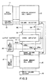
- Fig. 2 is a block diagram showing a structure of a memory device having a redundancy circuit.
- a regular memory cell array 10 in which a plurality of memory cells are formed in matrix form is provided.
- the row address of this regular memory cell array 10 is designated by a row decoder 11 and the column address of the memory cell array 10 is selected by a column selector 12 which is designated by a column decoder 13.
- the output date of the regular memory cell array is transferred to a sense amplifier via bit lines B11-BLn each having switching element Q1-Qn respectively to output an amplified data to an output buffer.
- a spare memory cell array 15 having a spare column selector 16 is also provided.
- Spare memory cell is designated by a spare row decoder 17 and write column decoder 18.
- the spare column selector 16 and the sense amplifier 14 is connected redundantly to a plurality of bit lines RBL1-RBLn each having switching element RQ1-RQn.
- the switching elements on the corresponding bit line and redundancy bit line are controlled by a bit line switching decoder 20 which enable either of the switching elements Q and RQ.
- the corresponding redundancy bit line is made enable by the bit line switching decoder 20 to use the spare memory cell as a normal cell.
- Each memory cell for example, memory cell C1, is constructed of an N-channel MOS transistor T3 for data reading, N-channel MOS transistor T1 for data writing, and fuse F1.
- Transistors T3 and T1 are serially connected between a spare bit line BL1 and ground line G1.
- One end of fuse F1 is connected to a write data line V E from which power is supplied,and the other end is connected to an interconnection between transistors T3 and T1.
- the gate electrode of transistor T3 is connected to a read word line WL, transistor T3 being made conductive when data is read.
- transistor T1 The gate electrode of transistor T1 is connected to a write word line L1. In writing data, transistor T1 is made conductive to blow fuse F1, and made non-conductive to not blow fuse F1.
- transistor T5 Also connected to the write data line V E is one end of an N-channel MOS transistor T5 whose other end is connected to the common ground line G1.
- the conduction of transistor T5 is controlled by a programming signal.
- a programming signal of low level is supplied and transistor T5 is made non-conductive.
- a programing signal of high level is supplied and transistor T5 is made conductive and the level of the write date line V E is lowered to a ground potential V SS .
- spare memory cell C2 connected to the same write data line V E is constructed of an N-channel MOS transistor T4 for data reading, N-channel MOS transistor T2 for data writing, and fuse F2.
- the write data line VE is set at the ground potential V SS .
- the read word line WL is set at high level to make transistors T3 and T4 conductive. Since fuse F1 has been blown, the spare bit line BL1 becomes high level. Whereas since fuse F2 has not been blown, the spare bit line BL2 becomes low level. In the above manner, the level of the spare bit line changes depending upon whether the fuse has been blown or not so that the data can read.
- transistors T1 and T2 for data writing have a threshold value Vth1.
- the word line L1 is set at the high level as shown in Fig. 1A, and the word line L2 is set at low level. Consequently, transistor T1 becomes conductive and transistor T2 becomes non-conductive so that the programming current I flows only through fuse F1.
- the programming current increase as shown in Fig. 1B and when it reaches a current value I1 at which fuse can be blown, fuse F1 is blown so that the programming current I rapidly reduces.
- the threshold voltage value of transistor T2 is set to larger than the potential difference V GS as shown is Fig. 1E. Therefore, transistor T2 maintains its non-conductive state, so that the program current I will not flow through fuse F2 and it will not be blown.
- the threshold voltage value of conventional transistors T1 and T2 have been set at Vth2 as shown in Fig. 1E.
- the potential difference V GS between the write word line L2 and ground line G1 at the time of fuse blowing becomes in excess of the threshold voltage value Vth2 of transistor T2. Accordingly, there arises a program that although the write word line L2 is set at the low lever, transistor T2 becomes conductive to allow flow of the programming current through fuse F2 and blow it.
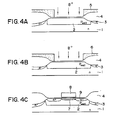
- Such a semicoductor memory device having a higher threshold voltage value Vth1 of transistors T1 and T2 can be manufactured by the following process. Sectional views of a memory cell at respective manufacturing steps are shown in Figs. 4A to 4C.
- a p-type well 2 in which at element is formed there are formed on the surface of an n-type semiconductor substrate 1, a p-type well 2 in which at element is formed, and a field oxide 4 for separating elements. Under the field oxide 4, there is formed an n ⁇ type field reversal preventing layer 3.
- a resist is coated over the entire surface. Thereafter, removal is performed for the resist above the region where n-channel transistor elements including n-channel transistors T1 and T2 with a higher threshold voltage value are being formed.
- the resist 5 obtained by such patterning as a mask boron ions (B+) are implanted as channel ions onto the surface of the element forming region. Thereafter the resist film 5 is removed.
- a resist is coated again over the whole surface. Thereafter removal is performed for the resist above the p-type transistor element forming region (not shown) and the resist above the region where n-channel transistors T1 and T2 having a higher threshold voltage value are being formed, to thereby obtain a resist 6 thus patterned.
- this resist 6 Byusing this resist 6, as a mask, boron ions (B+) are implanted as p-channel ions onto the surface of the element forming regions. Thereafter, the resist 6 is removed. On the surface of the region where transistors T1 and T2 are formed, boron ions (B+) have been implanted twice.
- Polycrystalline silicon is patterned on the surface and phosphorous are doped to the polycrystalline silicon layer to and lower the resistivity.
- RIE reactive ion etching
- a gate electrode 8 is formed by forming a resist (not shown) covering other than the region where a gate electrode is formed.
- RIE reactive ion etching
- the gate electrode 8 arsenic ions (As+) for example are implanted to form an N+ type diffusion layer 9 serving as a draw in or source region (Fig. 4C).
- the channel region 7 of transistors T1 and T2 has a higher p-type impurity concentration and threshold voltage value Vth1 than other n-channel transistors.
- the same type of ions are used for p-type channel ion implantation and for channel ion implantation of n-channel transistors.
- these ions are again implanted to transistors T1 and T2.
- the above embodiments are described by way of example only.
- the present invention is not limited thereto.
- N-channel MOS transistors are used as transistors for data writing in the embodiments
- p-channel MOS transistors may also be used.
- the threshold voltage value takes a negative value.
- the same advantageous effects can be obtained by setting the absolute value of the htreshold voltage value Vth to larger than the absolute value of the potential difference V GS between the write word line and ground line.
- the structure of the redundancy circuit may be different from that shown in Fig. 3, provided that the number of spare memory cells is two or more.
- the threshold voltage of fuse blowing control transistors are set such that they are not adversely affect by a potential change at a spare memory cell when another memory cell connected to the same power supply line is blown. Accordingly, it is possible to prevent an erroneous operation that a fuse which should not be blown is blown.
- Such a semiconductor device having a higher threshold voltage value can be manufactured without adding a new process by implanting ions twice to the channel region of fuse blowing control transistors, namely at the time when ions are implanted to the channel region of transistors having the same conductivity type of the fuse blowing control transistor and at the time when ions are implanted to the channel region of transistors having the opposite conductivity type, while reducing the manufacturing time and cost.
Landscapes
- Semiconductor Memories (AREA)
- Design And Manufacture Of Integrated Circuits (AREA)
- Read Only Memory (AREA)
Applications Claiming Priority (4)
| Application Number | Priority Date | Filing Date | Title |
|---|---|---|---|
| JP20916989 | 1989-08-11 | ||
| JP209169/89 | 1989-08-11 | ||
| JP2091104A JP2509730B2 (ja) | 1989-08-11 | 1990-04-05 | 半導体メモリ装置及びその製造方法 |
| JP91104/90 | 1990-04-05 |
Publications (3)
| Publication Number | Publication Date |
|---|---|
| EP0417484A2 true EP0417484A2 (de) | 1991-03-20 |
| EP0417484A3 EP0417484A3 (en) | 1992-01-02 |
| EP0417484B1 EP0417484B1 (de) | 1995-06-28 |
Family
ID=26432578
Family Applications (1)
| Application Number | Title | Priority Date | Filing Date |
|---|---|---|---|
| EP90115399A Expired - Lifetime EP0417484B1 (de) | 1989-08-11 | 1990-08-10 | Halbleiterspeichergerät und Verfahren zu dessen Herstellung |
Country Status (5)
| Country | Link |
|---|---|
| US (1) | US5257230A (de) |
| EP (1) | EP0417484B1 (de) |
| JP (1) | JP2509730B2 (de) |
| KR (1) | KR930010730B1 (de) |
| DE (1) | DE69020461T2 (de) |
Cited By (4)
| Publication number | Priority date | Publication date | Assignee | Title |
|---|---|---|---|---|
| EP0586114A3 (en) * | 1992-08-31 | 1996-10-16 | Sharp Kk | A semiconductor read only memory |
| US5764575A (en) * | 1995-09-29 | 1998-06-09 | Sharp Kabushiki Kaisha | Replacement semiconductor read-only memory |
| US5889711A (en) * | 1997-10-27 | 1999-03-30 | Macronix International Co., Ltd. | Memory redundancy for high density memory |
| GB2541961A (en) * | 2015-09-01 | 2017-03-08 | Lattice Semiconductor Corp | Multi-time programmable non-volatile memory cell |
Families Citing this family (12)
| Publication number | Priority date | Publication date | Assignee | Title |
|---|---|---|---|---|
| US5677888A (en) * | 1995-06-06 | 1997-10-14 | Integrated Device Technology, Inc. | Redundancy circuit for programmable integrated circuits |
| US6031771A (en) * | 1996-10-28 | 2000-02-29 | Macronix International Co., Ltd. | Memory redundancy circuit using single polysilicon floating gate transistors as redundancy elements |
| US5896327A (en) * | 1997-10-27 | 1999-04-20 | Macronix International Co., Ltd. | Memory redundancy circuit for high density memory with extra row and column for failed address storage |
| JP4639030B2 (ja) * | 2002-11-18 | 2011-02-23 | パナソニック株式会社 | 半導体記憶装置 |
| US7583554B2 (en) * | 2007-03-02 | 2009-09-01 | Freescale Semiconductor, Inc. | Integrated circuit fuse array |
| US8542549B2 (en) | 2011-08-08 | 2013-09-24 | Taiwan Semiconductor Manufacturing Company, Ltd. | Electrical fuse bit cell |
| US8760955B2 (en) * | 2011-10-21 | 2014-06-24 | Taiwan Semiconductor Manufacturing Company, Ltd. | Electrical fuse memory arrays |
| US8610243B2 (en) | 2011-12-09 | 2013-12-17 | Globalfoundries Inc. | Metal e-fuse with intermetallic compound programming mechanism and methods of making same |
| US20140268983A1 (en) * | 2013-03-15 | 2014-09-18 | GlobalFoundries, Inc. | Otprom array with leakage current cancelation for enhanced efuse sensing |
| KR102389817B1 (ko) * | 2016-01-28 | 2022-04-22 | 삼성전자주식회사 | 디스차아지 회로를 갖는 퓨즈 메모리 |
| US11088140B2 (en) | 2019-08-27 | 2021-08-10 | Nanya Technology Corporation | Multiple semiconductor elements with different threshold voltages |
| US11177010B1 (en) * | 2020-07-13 | 2021-11-16 | Qualcomm Incorporated | Bitcell for data redundancy |
Family Cites Families (7)
| Publication number | Priority date | Publication date | Assignee | Title |
|---|---|---|---|---|
| US4230504B1 (en) * | 1978-04-27 | 1997-03-04 | Texas Instruments Inc | Method of making implant programmable N-channel rom |
| JPS5843838B2 (ja) * | 1979-02-28 | 1983-09-29 | 富士通株式会社 | 読取り専用メモリ |
| JPS584969A (ja) * | 1981-06-30 | 1983-01-12 | Fujitsu Ltd | 半導体装置 |
| JPS60201598A (ja) * | 1984-03-23 | 1985-10-12 | Fujitsu Ltd | 半導体集積回路 |
| US4654830A (en) * | 1984-11-27 | 1987-03-31 | Monolithic Memories, Inc. | Method and structure for disabling and replacing defective memory in a PROM |
| JPH0235699A (ja) * | 1988-07-26 | 1990-02-06 | Nec Corp | 化合物半導体メモリデバイス |
| JPH0817039B2 (ja) * | 1988-08-19 | 1996-02-21 | 株式会社東芝 | 半導体メモリセル |
-
1990
- 1990-04-05 JP JP2091104A patent/JP2509730B2/ja not_active Expired - Lifetime
- 1990-08-10 DE DE69020461T patent/DE69020461T2/de not_active Expired - Fee Related
- 1990-08-10 EP EP90115399A patent/EP0417484B1/de not_active Expired - Lifetime
- 1990-08-11 KR KR1019900012363A patent/KR930010730B1/ko not_active Expired - Lifetime
- 1990-08-13 US US07/565,820 patent/US5257230A/en not_active Expired - Lifetime
Cited By (7)
| Publication number | Priority date | Publication date | Assignee | Title |
|---|---|---|---|---|
| EP0586114A3 (en) * | 1992-08-31 | 1996-10-16 | Sharp Kk | A semiconductor read only memory |
| US5764575A (en) * | 1995-09-29 | 1998-06-09 | Sharp Kabushiki Kaisha | Replacement semiconductor read-only memory |
| US5889711A (en) * | 1997-10-27 | 1999-03-30 | Macronix International Co., Ltd. | Memory redundancy for high density memory |
| EP0913868A1 (de) * | 1997-10-27 | 1999-05-06 | Macronix International Co., Ltd. | Speicherredundanzschaltung in einem Speicher hoher Dichte |
| GB2541961A (en) * | 2015-09-01 | 2017-03-08 | Lattice Semiconductor Corp | Multi-time programmable non-volatile memory cell |
| GB2541961B (en) * | 2015-09-01 | 2019-05-15 | Lattice Semiconductor Corp | Multi-time programmable non-volatile memory cell |
| US11295825B2 (en) | 2015-09-01 | 2022-04-05 | Lattice Semiconductor Corporation | Multi-time programmable non-volatile memory cell |
Also Published As
| Publication number | Publication date |
|---|---|
| EP0417484B1 (de) | 1995-06-28 |
| JPH03155652A (ja) | 1991-07-03 |
| JP2509730B2 (ja) | 1996-06-26 |
| KR910005459A (ko) | 1991-03-30 |
| DE69020461T2 (de) | 1996-01-11 |
| EP0417484A3 (en) | 1992-01-02 |
| KR930010730B1 (ko) | 1993-11-08 |
| DE69020461D1 (de) | 1995-08-03 |
| US5257230A (en) | 1993-10-26 |
Similar Documents
| Publication | Publication Date | Title |
|---|---|---|
| EP0417484B1 (de) | Halbleiterspeichergerät und Verfahren zu dessen Herstellung | |
| US6266269B1 (en) | Three terminal non-volatile memory element | |
| EP0627742B1 (de) | Halbleiterspeichereinrichtung | |
| US7227781B2 (en) | Semiconductor device provided with NAND strings and select gates having different gate lengths | |
| US5469397A (en) | Semiconductor memory device with a reference potential generator | |
| US5285069A (en) | Array of field effect transistors of different threshold voltages in same semiconductor integrated circuit | |
| JPS6061998A (ja) | リ−ドオンリメモリ用セル | |
| CN113963738A (zh) | 反熔丝装置及反熔丝单元的编程方法 | |
| US20020028548A1 (en) | Circuit and method of fabricating a memory cell for a static random access memory | |
| US5556800A (en) | Method of manufacturing a mask read only memory (ROM) for storing multi-value data | |
| US5377140A (en) | Cell for random access memory | |
| US6445041B1 (en) | Semiconductor memory cell array with reduced parasitic capacitance between word lines and bit lines | |
| EP0359204B1 (de) | Halbleiterspeicheranordnung, welche ein Herabsetzen der Anzahl mangelhafter Bits erlaubt | |
| JP3531081B2 (ja) | 半導体装置およびその製造方法、ならびにそれを利用したベリファイ方法 | |
| KR20040076358A (ko) | 휘발성 반도체 메모리의 제조공정에서 제조된 불휘발성메모리 셀 트랜지스터를 퓨즈소자로서 갖는 반도체 집적회로장치 | |
| US20050201158A1 (en) | EEPROM memory comprising a non-volatile register integrated into the memory array thereof | |
| US7227232B2 (en) | Contactless mask programmable ROM | |
| EP0263318B1 (de) | Halbleiterspeicher | |
| US20030198089A1 (en) | Semiconductor storage device | |
| GB2261090A (en) | String select arrangement in read only memory | |
| US6278629B1 (en) | Read-only memory and method for fabricating the same | |
| US4542482A (en) | Read only memory | |
| JPH0817196A (ja) | 半導体記憶装置 | |
| JPH05283610A (ja) | 半導体記憶装置 | |
| KR19990024590A (ko) | 마스크롬 및 그 제조방법 |
Legal Events
| Date | Code | Title | Description |
|---|---|---|---|
| PUAI | Public reference made under article 153(3) epc to a published international application that has entered the european phase |
Free format text: ORIGINAL CODE: 0009012 |
|
| 17P | Request for examination filed |
Effective date: 19900810 |
|
| AK | Designated contracting states |
Kind code of ref document: A2 Designated state(s): DE FR GB |
|
| PUAL | Search report despatched |
Free format text: ORIGINAL CODE: 0009013 |
|
| AK | Designated contracting states |
Kind code of ref document: A3 Designated state(s): DE FR GB |
|
| 17Q | First examination report despatched |
Effective date: 19940722 |
|
| GRAA | (expected) grant |
Free format text: ORIGINAL CODE: 0009210 |
|
| AK | Designated contracting states |
Kind code of ref document: B1 Designated state(s): DE FR GB |
|
| REF | Corresponds to: |
Ref document number: 69020461 Country of ref document: DE Date of ref document: 19950803 |
|
| ET | Fr: translation filed | ||
| PLBE | No opposition filed within time limit |
Free format text: ORIGINAL CODE: 0009261 |
|
| STAA | Information on the status of an ep patent application or granted ep patent |
Free format text: STATUS: NO OPPOSITION FILED WITHIN TIME LIMIT |
|
| 26N | No opposition filed | ||
| REG | Reference to a national code |
Ref country code: GB Ref legal event code: IF02 |
|
| PGFP | Annual fee paid to national office [announced via postgrant information from national office to epo] |
Ref country code: DE Payment date: 20070802 Year of fee payment: 18 |
|
| PGFP | Annual fee paid to national office [announced via postgrant information from national office to epo] |
Ref country code: GB Payment date: 20070809 Year of fee payment: 18 |
|
| PGFP | Annual fee paid to national office [announced via postgrant information from national office to epo] |
Ref country code: FR Payment date: 20070808 Year of fee payment: 18 |
|
| GBPC | Gb: european patent ceased through non-payment of renewal fee |
Effective date: 20080810 |
|
| REG | Reference to a national code |
Ref country code: FR Ref legal event code: ST Effective date: 20090430 |
|
| PG25 | Lapsed in a contracting state [announced via postgrant information from national office to epo] |
Ref country code: FR Free format text: LAPSE BECAUSE OF NON-PAYMENT OF DUE FEES Effective date: 20080901 Ref country code: DE Free format text: LAPSE BECAUSE OF NON-PAYMENT OF DUE FEES Effective date: 20090303 |
|
| PG25 | Lapsed in a contracting state [announced via postgrant information from national office to epo] |
Ref country code: GB Free format text: LAPSE BECAUSE OF NON-PAYMENT OF DUE FEES Effective date: 20080810 |