EP0418749A2 - Dispositif à circuit intÀ©gré comprenant des connexions améliorées entre les broches et la puce de matériau semi-conducteur - Google Patents
Dispositif à circuit intÀ©gré comprenant des connexions améliorées entre les broches et la puce de matériau semi-conducteur Download PDFInfo
- Publication number
- EP0418749A2 EP0418749A2 EP90117744A EP90117744A EP0418749A2 EP 0418749 A2 EP0418749 A2 EP 0418749A2 EP 90117744 A EP90117744 A EP 90117744A EP 90117744 A EP90117744 A EP 90117744A EP 0418749 A2 EP0418749 A2 EP 0418749A2
- Authority
- EP
- European Patent Office
- Prior art keywords
- gold
- wires
- pins
- connections
- aluminum
- Prior art date
- Legal status (The legal status is an assumption and is not a legal conclusion. Google has not performed a legal analysis and makes no representation as to the accuracy of the status listed.)
- Granted
Links
Images
Classifications
-
- H—ELECTRICITY
- H10—SEMICONDUCTOR DEVICES; ELECTRIC SOLID-STATE DEVICES NOT OTHERWISE PROVIDED FOR
- H10W—GENERIC PACKAGES, INTERCONNECTIONS, CONNECTORS OR OTHER CONSTRUCTIONAL DETAILS OF DEVICES COVERED BY CLASS H10
- H10W70/00—Package substrates; Interposers; Redistribution layers [RDL]
- H10W70/40—Leadframes
- H10W70/421—Shapes or dispositions
-
- H—ELECTRICITY
- H10—SEMICONDUCTOR DEVICES; ELECTRIC SOLID-STATE DEVICES NOT OTHERWISE PROVIDED FOR
- H10W—GENERIC PACKAGES, INTERCONNECTIONS, CONNECTORS OR OTHER CONSTRUCTIONAL DETAILS OF DEVICES COVERED BY CLASS H10
- H10W72/00—Interconnections or connectors in packages
- H10W72/50—Bond wires
-
- H—ELECTRICITY
- H10—SEMICONDUCTOR DEVICES; ELECTRIC SOLID-STATE DEVICES NOT OTHERWISE PROVIDED FOR
- H10W—GENERIC PACKAGES, INTERCONNECTIONS, CONNECTORS OR OTHER CONSTRUCTIONAL DETAILS OF DEVICES COVERED BY CLASS H10
- H10W72/00—Interconnections or connectors in packages
- H10W72/90—Bond pads, in general
-
- H—ELECTRICITY
- H10—SEMICONDUCTOR DEVICES; ELECTRIC SOLID-STATE DEVICES NOT OTHERWISE PROVIDED FOR
- H10W—GENERIC PACKAGES, INTERCONNECTIONS, CONNECTORS OR OTHER CONSTRUCTIONAL DETAILS OF DEVICES COVERED BY CLASS H10
- H10W72/00—Interconnections or connectors in packages
- H10W72/071—Connecting or disconnecting
- H10W72/075—Connecting or disconnecting of bond wires
-
- H—ELECTRICITY
- H10—SEMICONDUCTOR DEVICES; ELECTRIC SOLID-STATE DEVICES NOT OTHERWISE PROVIDED FOR
- H10W—GENERIC PACKAGES, INTERCONNECTIONS, CONNECTORS OR OTHER CONSTRUCTIONAL DETAILS OF DEVICES COVERED BY CLASS H10
- H10W72/00—Interconnections or connectors in packages
- H10W72/071—Connecting or disconnecting
- H10W72/075—Connecting or disconnecting of bond wires
- H10W72/07531—Techniques
- H10W72/07532—Compression bonding, e.g. thermocompression bonding
- H10W72/07533—Ultrasonic bonding, e.g. thermosonic bonding
-
- H—ELECTRICITY
- H10—SEMICONDUCTOR DEVICES; ELECTRIC SOLID-STATE DEVICES NOT OTHERWISE PROVIDED FOR
- H10W—GENERIC PACKAGES, INTERCONNECTIONS, CONNECTORS OR OTHER CONSTRUCTIONAL DETAILS OF DEVICES COVERED BY CLASS H10
- H10W72/00—Interconnections or connectors in packages
- H10W72/071—Connecting or disconnecting
- H10W72/075—Connecting or disconnecting of bond wires
- H10W72/07551—Connecting or disconnecting of bond wires characterised by changes in properties of the bond wires during the connecting
- H10W72/07552—Connecting or disconnecting of bond wires characterised by changes in properties of the bond wires during the connecting changes in structures or sizes
-
- H—ELECTRICITY
- H10—SEMICONDUCTOR DEVICES; ELECTRIC SOLID-STATE DEVICES NOT OTHERWISE PROVIDED FOR
- H10W—GENERIC PACKAGES, INTERCONNECTIONS, CONNECTORS OR OTHER CONSTRUCTIONAL DETAILS OF DEVICES COVERED BY CLASS H10
- H10W72/00—Interconnections or connectors in packages
- H10W72/071—Connecting or disconnecting
- H10W72/075—Connecting or disconnecting of bond wires
- H10W72/07551—Connecting or disconnecting of bond wires characterised by changes in properties of the bond wires during the connecting
- H10W72/07553—Connecting or disconnecting of bond wires characterised by changes in properties of the bond wires during the connecting changes in shapes
-
- H—ELECTRICITY
- H10—SEMICONDUCTOR DEVICES; ELECTRIC SOLID-STATE DEVICES NOT OTHERWISE PROVIDED FOR
- H10W—GENERIC PACKAGES, INTERCONNECTIONS, CONNECTORS OR OTHER CONSTRUCTIONAL DETAILS OF DEVICES COVERED BY CLASS H10
- H10W72/00—Interconnections or connectors in packages
- H10W72/071—Connecting or disconnecting
- H10W72/075—Connecting or disconnecting of bond wires
- H10W72/07551—Connecting or disconnecting of bond wires characterised by changes in properties of the bond wires during the connecting
- H10W72/07555—Connecting or disconnecting of bond wires characterised by changes in properties of the bond wires during the connecting changes in materials
-
- H—ELECTRICITY
- H10—SEMICONDUCTOR DEVICES; ELECTRIC SOLID-STATE DEVICES NOT OTHERWISE PROVIDED FOR
- H10W—GENERIC PACKAGES, INTERCONNECTIONS, CONNECTORS OR OTHER CONSTRUCTIONAL DETAILS OF DEVICES COVERED BY CLASS H10
- H10W72/00—Interconnections or connectors in packages
- H10W72/50—Bond wires
- H10W72/521—Structures or relative sizes of bond wires
- H10W72/527—Multiple bond wires having different sizes
-
- H—ELECTRICITY
- H10—SEMICONDUCTOR DEVICES; ELECTRIC SOLID-STATE DEVICES NOT OTHERWISE PROVIDED FOR
- H10W—GENERIC PACKAGES, INTERCONNECTIONS, CONNECTORS OR OTHER CONSTRUCTIONAL DETAILS OF DEVICES COVERED BY CLASS H10
- H10W72/00—Interconnections or connectors in packages
- H10W72/50—Bond wires
- H10W72/531—Shapes of wire connectors
- H10W72/5363—Shapes of wire connectors the connected ends being wedge-shaped
-
- H—ELECTRICITY
- H10—SEMICONDUCTOR DEVICES; ELECTRIC SOLID-STATE DEVICES NOT OTHERWISE PROVIDED FOR
- H10W—GENERIC PACKAGES, INTERCONNECTIONS, CONNECTORS OR OTHER CONSTRUCTIONAL DETAILS OF DEVICES COVERED BY CLASS H10
- H10W72/00—Interconnections or connectors in packages
- H10W72/50—Bond wires
- H10W72/531—Shapes of wire connectors
- H10W72/537—Multiple bond wires having different shapes
-
- H—ELECTRICITY
- H10—SEMICONDUCTOR DEVICES; ELECTRIC SOLID-STATE DEVICES NOT OTHERWISE PROVIDED FOR
- H10W—GENERIC PACKAGES, INTERCONNECTIONS, CONNECTORS OR OTHER CONSTRUCTIONAL DETAILS OF DEVICES COVERED BY CLASS H10
- H10W72/00—Interconnections or connectors in packages
- H10W72/50—Bond wires
- H10W72/541—Dispositions of bond wires
- H10W72/5445—Dispositions of bond wires being orthogonal to a side surface of the chip, e.g. parallel arrangements
-
- H—ELECTRICITY
- H10—SEMICONDUCTOR DEVICES; ELECTRIC SOLID-STATE DEVICES NOT OTHERWISE PROVIDED FOR
- H10W—GENERIC PACKAGES, INTERCONNECTIONS, CONNECTORS OR OTHER CONSTRUCTIONAL DETAILS OF DEVICES COVERED BY CLASS H10
- H10W72/00—Interconnections or connectors in packages
- H10W72/50—Bond wires
- H10W72/541—Dispositions of bond wires
- H10W72/5449—Dispositions of bond wires not being orthogonal to a side surface of the chip, e.g. fan-out arrangements
-
- H—ELECTRICITY
- H10—SEMICONDUCTOR DEVICES; ELECTRIC SOLID-STATE DEVICES NOT OTHERWISE PROVIDED FOR
- H10W—GENERIC PACKAGES, INTERCONNECTIONS, CONNECTORS OR OTHER CONSTRUCTIONAL DETAILS OF DEVICES COVERED BY CLASS H10
- H10W72/00—Interconnections or connectors in packages
- H10W72/50—Bond wires
- H10W72/551—Materials of bond wires
- H10W72/552—Materials of bond wires comprising metals or metalloids, e.g. silver
- H10W72/5522—Materials of bond wires comprising metals or metalloids, e.g. silver comprising gold [Au]
-
- H—ELECTRICITY
- H10—SEMICONDUCTOR DEVICES; ELECTRIC SOLID-STATE DEVICES NOT OTHERWISE PROVIDED FOR
- H10W—GENERIC PACKAGES, INTERCONNECTIONS, CONNECTORS OR OTHER CONSTRUCTIONAL DETAILS OF DEVICES COVERED BY CLASS H10
- H10W72/00—Interconnections or connectors in packages
- H10W72/50—Bond wires
- H10W72/551—Materials of bond wires
- H10W72/552—Materials of bond wires comprising metals or metalloids, e.g. silver
- H10W72/5524—Materials of bond wires comprising metals or metalloids, e.g. silver comprising aluminium [Al]
-
- H—ELECTRICITY
- H10—SEMICONDUCTOR DEVICES; ELECTRIC SOLID-STATE DEVICES NOT OTHERWISE PROVIDED FOR
- H10W—GENERIC PACKAGES, INTERCONNECTIONS, CONNECTORS OR OTHER CONSTRUCTIONAL DETAILS OF DEVICES COVERED BY CLASS H10
- H10W72/00—Interconnections or connectors in packages
- H10W72/50—Bond wires
- H10W72/551—Materials of bond wires
- H10W72/552—Materials of bond wires comprising metals or metalloids, e.g. silver
- H10W72/5525—Materials of bond wires comprising metals or metalloids, e.g. silver comprising copper [Cu]
-
- H—ELECTRICITY
- H10—SEMICONDUCTOR DEVICES; ELECTRIC SOLID-STATE DEVICES NOT OTHERWISE PROVIDED FOR
- H10W—GENERIC PACKAGES, INTERCONNECTIONS, CONNECTORS OR OTHER CONSTRUCTIONAL DETAILS OF DEVICES COVERED BY CLASS H10
- H10W72/00—Interconnections or connectors in packages
- H10W72/50—Bond wires
- H10W72/551—Materials of bond wires
- H10W72/557—Multiple bond wires having different materials
-
- H—ELECTRICITY
- H10—SEMICONDUCTOR DEVICES; ELECTRIC SOLID-STATE DEVICES NOT OTHERWISE PROVIDED FOR
- H10W—GENERIC PACKAGES, INTERCONNECTIONS, CONNECTORS OR OTHER CONSTRUCTIONAL DETAILS OF DEVICES COVERED BY CLASS H10
- H10W72/00—Interconnections or connectors in packages
- H10W72/50—Bond wires
- H10W72/59—Bond pads specially adapted therefor
-
- H—ELECTRICITY
- H10—SEMICONDUCTOR DEVICES; ELECTRIC SOLID-STATE DEVICES NOT OTHERWISE PROVIDED FOR
- H10W—GENERIC PACKAGES, INTERCONNECTIONS, CONNECTORS OR OTHER CONSTRUCTIONAL DETAILS OF DEVICES COVERED BY CLASS H10
- H10W72/00—Interconnections or connectors in packages
- H10W72/90—Bond pads, in general
- H10W72/921—Structures or relative sizes of bond pads
- H10W72/926—Multiple bond pads having different sizes
-
- H—ELECTRICITY
- H10—SEMICONDUCTOR DEVICES; ELECTRIC SOLID-STATE DEVICES NOT OTHERWISE PROVIDED FOR
- H10W—GENERIC PACKAGES, INTERCONNECTIONS, CONNECTORS OR OTHER CONSTRUCTIONAL DETAILS OF DEVICES COVERED BY CLASS H10
- H10W72/00—Interconnections or connectors in packages
- H10W72/90—Bond pads, in general
- H10W72/951—Materials of bond pads
-
- H—ELECTRICITY
- H10—SEMICONDUCTOR DEVICES; ELECTRIC SOLID-STATE DEVICES NOT OTHERWISE PROVIDED FOR
- H10W—GENERIC PACKAGES, INTERCONNECTIONS, CONNECTORS OR OTHER CONSTRUCTIONAL DETAILS OF DEVICES COVERED BY CLASS H10
- H10W72/00—Interconnections or connectors in packages
- H10W72/90—Bond pads, in general
- H10W72/951—Materials of bond pads
- H10W72/952—Materials of bond pads comprising metals or metalloids, e.g. PbSn, Ag or Cu
-
- H—ELECTRICITY
- H10—SEMICONDUCTOR DEVICES; ELECTRIC SOLID-STATE DEVICES NOT OTHERWISE PROVIDED FOR
- H10W—GENERIC PACKAGES, INTERCONNECTIONS, CONNECTORS OR OTHER CONSTRUCTIONAL DETAILS OF DEVICES COVERED BY CLASS H10
- H10W90/00—Package configurations
- H10W90/701—Package configurations characterised by the relative positions of pads or connectors relative to package parts
- H10W90/751—Package configurations characterised by the relative positions of pads or connectors relative to package parts of bond wires
- H10W90/756—Package configurations characterised by the relative positions of pads or connectors relative to package parts of bond wires between a chip and a stacked lead frame, conducting package substrate or heat sink
Definitions
- the present invention relates to an integrated device having improved connections between the pins and the semiconductor material chip which integrates electronic components.
- the semiconductor material chip which integrates electronic components is connected to the pins which protrude externally from the housing (package) of the device by means of wires which are soldered on appropriate pads of the chip at one end and to an end of the pins at the other.
- wires are currently made of gold or aluminum (or of alloys with a prevalence of gold and aluminum).
- gold is the preferred material, by virtue of its characteristics of ductility, workability, conduction etc. which make it the most suitable for connections.
- gold wires cannot be used if they must carry high currents (power integrated circuits). As the current rises, it is in fact necessary to provide wires with a larger diameter, but gold wires with a diameter of more than 50 ⁇ m would have an excessively high cost.
- the integrated circuit comprises only low-power components (for "signal" control)
- gold wires are preferably used for the connections, whereas aluminum wires are used in the case of power integrated circuits.
- the devices in which aluminum wires of different diameters depending on the currents to be conducted are provided require in any case large areas on the chip for the execution of contact pads with dimensions adequate for the diameter of the wires used and to the soldering technique employed.
- the problem affects in particular integrated devices which have a large number of pins, in which chips with large surfaces must currently be provided in order to have enough room for the soldering of the connections.
- Another disadvantage of this technique is the need to use different soldering machines according to the diameter of the wire to be soldered.
- the aim of the present invention is to provide an integrated device with improved connections between the pins and the semiconductr material chip which integrates electronic components, which solves the disadvantages of the known art and in particular does not require large soldering areas on the chip.
- a particular object of the present invention is to provide connections for integrated circuits which have high reliability and verifiability.
- Not least object of the present invention is to provide connections for integrated circuits which require, for their manufacture, the use of devices or procedures which are already in use in the electronics industry.
- the invention proposes the use of different materials and in particular the use of different diameters for the signal connections and for the power connections.
- the power connections are provided by means of low-cost wires (pure aluminum or Al alloys, such as for example Al/Mg) of adequate diameter (7, 10, 15 mil), whereas the signal connections are provided by means of wires of material normally used for signal connections (gold or alloys of gold with prevalence of gold) with a small diameter (between 1 and 2 mil).
- soldering machines specialized for the type of wire used, and specifically, “thermosonic”-technology machines have been used for gold wires, whereas “ultrasonic”-technology machines have been used for aluminum wires.
- the pins are selectively gold-plated; specifically, the internal parts intended to be enclosed in the package are gold-plated, so that the gold plating remains inside the package after its closure.
- This selective plating is performed prior to the mechanical connection between the lead frame and the chip supporting slag.
- the plating is performed electrolytically by means of plastic protection masks which cover the parts which are not to be gold-plated.
- the invention applies both to devices with non-planar lead frame and to devices with planar lead frame.
- the Applicant has developed two possible procedures for the gold-plating of the pins.
- the lead frame is initially degreased by immersion in a sodium hydrate bath and is then washed, and the material is revived in a bath of hydrochloric acid.
- the lead frame is coated with a very thin layer of copper by immersion in a bath (copper flashing), is then coated with a thin layer of nickel (1 ⁇ m) and is then plated with electrolytic gold (0.6 ⁇ m gold flashing).
- the nickel coating is performed first, followed by the copper coating and by the gold plating.
- the thickness of the layers can also vary within a wide range, for example thicknesses comprised between 0.1 and 3 ⁇ m for nickel and between 0.4 and 2.5 ⁇ m for gold have yielded good results.
- the devices executed according to the invention have been subjected to reliability tests. Said tests have been performed on both assembled and encapsulated units and on assembled and non-encapsulated units and have yielded excellent results. In particular, 336-hour tests at PPT (Pressure Pot Temperature) on assembled and non-encapsulated units have shown no deviations with respect to the results of pull tests yielded prior to the PPT tests.
- PPT Pressure Pot Temperature
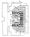
- the reference numeral 1 indicates the supporting slag of the chip 2, which is already mechanically fixed to the lead frame 3, of which only a part is shown in the figure and supports the pins 5 related to the illustrated chip 2 (15 pins in the illustrated case).
- the pins 5 are divided into a portion 6, which is plated in a conventional manner and is therefore tin-plated, and into a gold-plated portion 7, as indicated schematically in the figure by the shading.
- 13 connections out of 15 are used for the signal and have therefore been provided by means of thin gold wires 8, whereas the remaining two connections are power connections and are therefore provided by means of thicker aluminum wire 9.
- the figure also illustrates the contact pads 10 for the signal and the contact pads 11 for the power. As can be seen, the pads 11 are considerably larger than the pads 10.
- the dot-and-dash line 13 indicates the contour of the package, which as can be seen is intended to completely surround the gold-plated part 7 of the pins, which therefore cannot be accessed outside the package, at the end of assembly.
- the invention fully achieves the proposed aim and objects.
- the space required for soldering said wires on the chip is in fact reduced, and the use of different diameters for the different materials, and specifically thin gold wires for the signal and thick aluminum wires for the power, furthermore allows a substantial reduction in the area of the soldering pads with respect to the case in which only aluminum wires are used.
- the solution according to the invention is furthermore completely reliable.
- the "multi-wire" technique can be limited to the use of only two wires in parallel (which correspond to a maximum current of 5 A, by providing the connections which must carry higher currents in aluminum), and this still allows safe discrimination between unbroken connections and defective ones, without thus compromising the reliability of the interconnections.
- the invention thus conceived is susceptible to numerous modifications and variations, all of which are within the scope of the inventive concept.
- the fact is stressed that though reference to gold and aluminum wires has been made in the description, the invention also relates to the alloys of said metals.
- Other materials such as for example copper, which is currently being studied) can furthermore also be considered for the execution of the connections between the chip and the pins of integrated devices according to the invention, if they are considered suitable for the purpose and their use is considered advantageous.
Landscapes
- Wire Bonding (AREA)
- Cooling Or The Like Of Semiconductors Or Solid State Devices (AREA)
- Lead Frames For Integrated Circuits (AREA)
Applications Claiming Priority (2)
| Application Number | Priority Date | Filing Date | Title |
|---|---|---|---|
| IT2178389 | 1989-09-21 | ||
| IT8921783A IT1233008B (it) | 1989-09-21 | 1989-09-21 | Dispositivo integrato con connessioni perfezionate fra i terminali e la piastrina di materiale semiconduttore integrante componenti elettronici |
Publications (3)
| Publication Number | Publication Date |
|---|---|
| EP0418749A2 true EP0418749A2 (fr) | 1991-03-27 |
| EP0418749A3 EP0418749A3 (en) | 1991-05-29 |
| EP0418749B1 EP0418749B1 (fr) | 1995-11-29 |
Family
ID=11186786
Family Applications (1)
| Application Number | Title | Priority Date | Filing Date |
|---|---|---|---|
| EP90117744A Expired - Lifetime EP0418749B1 (fr) | 1989-09-21 | 1990-09-14 | Dispositif à circuit intégré comprenant des connexions améliorées entre les broches et la puce de matériau semi-conducteur |
Country Status (6)
| Country | Link |
|---|---|
| US (2) | US5113239A (fr) |
| EP (1) | EP0418749B1 (fr) |
| JP (1) | JPH03131043A (fr) |
| KR (1) | KR910007118A (fr) |
| DE (1) | DE69023858T2 (fr) |
| IT (1) | IT1233008B (fr) |
Cited By (6)
| Publication number | Priority date | Publication date | Assignee | Title |
|---|---|---|---|---|
| EP0446937B1 (fr) * | 1990-03-15 | 1996-06-05 | Kabushiki Kaisha Toshiba | Procédé de formation d'un dispositif semi-conducteur utilisant des fils soudés en matériaux différents |
| EP0731505A3 (fr) * | 1995-03-06 | 1998-04-15 | Motorola, Inc. | Cadre de connexion pour semi-conducteur et procédé de fabrication |
| WO1998021751A3 (fr) * | 1996-11-11 | 1998-07-09 | Siemens Ag | Optimisation de la connexion de puissance entre une puce et un cadre conducteur pour sectionneur de puissance |
| WO2007107964A1 (fr) * | 2006-03-23 | 2007-09-27 | Nxp B.V. | Boitier soude par fil ameliore electriquement |
| WO2009088803A1 (fr) * | 2008-01-03 | 2009-07-16 | Linear Technology Corporation | Structure souple de fixation de fil sans contact et méthodologie pour dispositif à semi-conducteur |
| US7902665B2 (en) | 2008-09-02 | 2011-03-08 | Linear Technology Corporation | Semiconductor device having a suspended isolating interconnect |
Families Citing this family (14)
| Publication number | Priority date | Publication date | Assignee | Title |
|---|---|---|---|---|
| US5281772A (en) * | 1991-10-28 | 1994-01-25 | Delco Electronics Corporation | Electrical connector having energy-formed solder stops and methods of making and using the same |
| JP2783133B2 (ja) * | 1993-09-29 | 1998-08-06 | 松下電器産業株式会社 | ワイヤボンディング前処理方法 |
| US7073254B2 (en) | 1993-11-16 | 2006-07-11 | Formfactor, Inc. | Method for mounting a plurality of spring contact elements |
| EP0722198A3 (fr) * | 1995-01-10 | 1996-10-23 | Texas Instruments Inc | Fil avec une connexion intégrée |
| US8033838B2 (en) | 1996-02-21 | 2011-10-11 | Formfactor, Inc. | Microelectronic contact structure |
| US6997931B2 (en) * | 2001-02-02 | 2006-02-14 | Lsi Solutions, Inc. | System for endoscopic suturing |
| US20030155635A1 (en) * | 2002-02-21 | 2003-08-21 | Matsushita Electric Industrial Co., Ltd. | Semiconductor device, method for designing the same and recording medium that can be read by computer in which program for designing semiconductor device is recorded |
| US7304393B1 (en) * | 2004-03-24 | 2007-12-04 | Microtune (Texas), L.P. | System and method for coupling internal circuitry of an integrated circuit to the integrated circuit's package pins |
| WO2006018671A1 (fr) * | 2004-08-19 | 2006-02-23 | Infineon Technologies Ag | Boitier a grilles de connexion a semi-conducteurs et a fils mixtes |
| JP5011879B2 (ja) * | 2006-08-09 | 2012-08-29 | サンケン電気株式会社 | 半導体装置及びリードフレーム組立体の製法 |
| US8125060B2 (en) * | 2006-12-08 | 2012-02-28 | Infineon Technologies Ag | Electronic component with layered frame |
| JP2008235911A (ja) * | 2008-03-26 | 2008-10-02 | Murata Mfg Co Ltd | 低温焼成セラミック回路基板及びその製造方法 |
| JP6121692B2 (ja) * | 2012-11-05 | 2017-04-26 | ルネサスエレクトロニクス株式会社 | 半導体装置およびその製造方法 |
| JP2018128487A (ja) * | 2017-02-06 | 2018-08-16 | セイコーエプソン株式会社 | 電気光学パネル、電気光学装置および電子機器 |
Family Cites Families (8)
| Publication number | Priority date | Publication date | Assignee | Title |
|---|---|---|---|---|
| JPS5434678A (en) * | 1977-08-22 | 1979-03-14 | Matsushita Electronics Corp | Semiconductor device |
| JPS553641A (en) * | 1978-06-23 | 1980-01-11 | Hitachi Ltd | Lead frame |
| US4458297A (en) * | 1981-01-16 | 1984-07-03 | Mosaic Systems, Inc. | Universal interconnection substrate |
| JPS588951A (ja) * | 1981-07-09 | 1983-01-19 | Sanyo Electric Co Ltd | 太陽熱貯湯装置 |
| JPS59172757A (ja) * | 1983-03-22 | 1984-09-29 | Matsushita Electronics Corp | 半導体装置 |
| JPS6189643A (ja) * | 1984-10-09 | 1986-05-07 | Toshiba Corp | 半導体装置及びその製造方法 |
| JPS6396947A (ja) * | 1986-10-13 | 1988-04-27 | Mitsubishi Electric Corp | 半導体装置用リ−ドフレ−ム |
| US4818895A (en) * | 1987-11-13 | 1989-04-04 | Kaufman Lance R | Direct current sense lead |
-
1989
- 1989-09-21 IT IT8921783A patent/IT1233008B/it active
-
1990
- 1990-09-14 EP EP90117744A patent/EP0418749B1/fr not_active Expired - Lifetime
- 1990-09-14 DE DE69023858T patent/DE69023858T2/de not_active Expired - Fee Related
- 1990-09-17 US US07/583,271 patent/US5113239A/en not_active Expired - Lifetime
- 1990-09-20 KR KR1019900014960A patent/KR910007118A/ko not_active Ceased
- 1990-09-20 JP JP2254039A patent/JPH03131043A/ja active Pending
-
1992
- 1992-04-13 US US07/867,646 patent/US5165590A/en not_active Expired - Lifetime
Cited By (9)
| Publication number | Priority date | Publication date | Assignee | Title |
|---|---|---|---|---|
| EP0446937B1 (fr) * | 1990-03-15 | 1996-06-05 | Kabushiki Kaisha Toshiba | Procédé de formation d'un dispositif semi-conducteur utilisant des fils soudés en matériaux différents |
| EP0731505A3 (fr) * | 1995-03-06 | 1998-04-15 | Motorola, Inc. | Cadre de connexion pour semi-conducteur et procédé de fabrication |
| WO1998021751A3 (fr) * | 1996-11-11 | 1998-07-09 | Siemens Ag | Optimisation de la connexion de puissance entre une puce et un cadre conducteur pour sectionneur de puissance |
| WO2007107964A1 (fr) * | 2006-03-23 | 2007-09-27 | Nxp B.V. | Boitier soude par fil ameliore electriquement |
| US8203219B2 (en) | 2006-03-23 | 2012-06-19 | Taiwan Semiconductor Manufacturing Company, Ltd. | Electrically enhanced wirebond package |
| WO2009088803A1 (fr) * | 2008-01-03 | 2009-07-16 | Linear Technology Corporation | Structure souple de fixation de fil sans contact et méthodologie pour dispositif à semi-conducteur |
| US7960845B2 (en) | 2008-01-03 | 2011-06-14 | Linear Technology Corporation | Flexible contactless wire bonding structure and methodology for semiconductor device |
| US8269355B2 (en) | 2008-01-03 | 2012-09-18 | Linear Technology Corporation | Flexible contactless wire bonding structure and methodology for semiconductor device |
| US7902665B2 (en) | 2008-09-02 | 2011-03-08 | Linear Technology Corporation | Semiconductor device having a suspended isolating interconnect |
Also Published As
| Publication number | Publication date |
|---|---|
| US5113239A (en) | 1992-05-12 |
| DE69023858T2 (de) | 1996-08-22 |
| EP0418749A3 (en) | 1991-05-29 |
| DE69023858D1 (de) | 1996-01-11 |
| EP0418749B1 (fr) | 1995-11-29 |
| IT1233008B (it) | 1992-03-14 |
| JPH03131043A (ja) | 1991-06-04 |
| US5165590A (en) | 1992-11-24 |
| IT8921783A0 (it) | 1989-09-21 |
| KR910007118A (ko) | 1991-04-30 |
Similar Documents
| Publication | Publication Date | Title |
|---|---|---|
| EP0418749B1 (fr) | Dispositif à circuit intégré comprenant des connexions améliorées entre les broches et la puce de matériau semi-conducteur | |
| JP4672373B2 (ja) | 半導体装置用ボンディングワイヤ | |
| CN101410964A (zh) | 用于半导体qfn/son器件的铝引线框架 | |
| JP2000277672A (ja) | リードフレーム及びその製法と半導体デバイス | |
| US5540378A (en) | Method for the assembly of an electronic package | |
| TWI817015B (zh) | 金被覆接合線及其製造方法、半導體線接合構造及半導體裝置 | |
| US6139977A (en) | Palladium surface coating suitable for wirebonding and process for forming palladium surface coatings | |
| US8703544B2 (en) | Electronic component employing a layered frame | |
| US4590672A (en) | Package for electronic device and method for producing same | |
| WO2023177604A1 (fr) | Dispositif électronique à fiabilité de niveau de carte améliorée | |
| JP2925815B2 (ja) | 半導体チップ実装用リードフレームとその製造方法 | |
| JPH11176864A (ja) | 半導体パッケージ | |
| JPH07326701A (ja) | 電気電子部品用導電材、リードフレ−ム及びそれを使用した半導体集積回路 | |
| JPH10251860A (ja) | 金/ニッケル/ニッケル3層めっき銅合金電子部品およびその製造方法 | |
| KR100702956B1 (ko) | 반도체 팩키지용 리드프레임 및 그 제조 방법 | |
| JPH0590465A (ja) | 半導体装置 | |
| KR100225778B1 (ko) | 리드 프레임을 이용한 반도체 팩키지 | |
| JPH06302756A (ja) | 半導体装置用リードフレーム | |
| JPH09331009A (ja) | リードフレームとリードフレーム部材、およびこれらを用いた樹脂封止型半導体装置 | |
| JP2004282103A (ja) | リードフレームの部分貴金属めっき方法 | |
| KR19980074509A (ko) | 다중 도금층을 가진 반도체 리드프레임 | |
| WO2024226118A1 (fr) | Dispositif électronique comprenant une bicouche d'étain et de nickel tungstène plaquée post-moulage pour une fiabilité de niveau de carte améliorée | |
| JPH04174546A (ja) | 銅合金製半導体リードフレームの製造方法 | |
| JPH09116065A (ja) | リードフレーム | |
| JPH0770665B2 (ja) | 半導体装置の製造方法 |
Legal Events
| Date | Code | Title | Description |
|---|---|---|---|
| PUAI | Public reference made under article 153(3) epc to a published international application that has entered the european phase |
Free format text: ORIGINAL CODE: 0009012 |
|
| AK | Designated contracting states |
Kind code of ref document: A2 Designated state(s): DE FR GB NL SE |
|
| PUAL | Search report despatched |
Free format text: ORIGINAL CODE: 0009013 |
|
| AK | Designated contracting states |
Kind code of ref document: A3 Designated state(s): DE FR GB NL SE |
|
| 17P | Request for examination filed |
Effective date: 19911017 |
|
| 17Q | First examination report despatched |
Effective date: 19940506 |
|
| GRAA | (expected) grant |
Free format text: ORIGINAL CODE: 0009210 |
|
| AK | Designated contracting states |
Kind code of ref document: B1 Designated state(s): DE FR GB NL SE |
|
| PG25 | Lapsed in a contracting state [announced via postgrant information from national office to epo] |
Ref country code: NL Free format text: LAPSE BECAUSE OF FAILURE TO SUBMIT A TRANSLATION OF THE DESCRIPTION OR TO PAY THE FEE WITHIN THE PRESCRIBED TIME-LIMIT Effective date: 19951129 |
|
| REF | Corresponds to: |
Ref document number: 69023858 Country of ref document: DE Date of ref document: 19960111 |
|
| PG25 | Lapsed in a contracting state [announced via postgrant information from national office to epo] |
Ref country code: SE Effective date: 19960229 |
|
| ET | Fr: translation filed | ||
| NLV1 | Nl: lapsed or annulled due to failure to fulfill the requirements of art. 29p and 29m of the patents act | ||
| PLBE | No opposition filed within time limit |
Free format text: ORIGINAL CODE: 0009261 |
|
| STAA | Information on the status of an ep patent application or granted ep patent |
Free format text: STATUS: NO OPPOSITION FILED WITHIN TIME LIMIT |
|
| 26N | No opposition filed | ||
| REG | Reference to a national code |
Ref country code: FR Ref legal event code: D6 |
|
| REG | Reference to a national code |
Ref country code: GB Ref legal event code: IF02 |
|
| PGFP | Annual fee paid to national office [announced via postgrant information from national office to epo] |
Ref country code: FR Payment date: 20020910 Year of fee payment: 13 |
|
| PGFP | Annual fee paid to national office [announced via postgrant information from national office to epo] |
Ref country code: GB Payment date: 20020911 Year of fee payment: 13 |
|
| PGFP | Annual fee paid to national office [announced via postgrant information from national office to epo] |
Ref country code: DE Payment date: 20020918 Year of fee payment: 13 |
|
| PG25 | Lapsed in a contracting state [announced via postgrant information from national office to epo] |
Ref country code: GB Free format text: LAPSE BECAUSE OF NON-PAYMENT OF DUE FEES Effective date: 20030914 |
|
| PG25 | Lapsed in a contracting state [announced via postgrant information from national office to epo] |
Ref country code: DE Free format text: LAPSE BECAUSE OF NON-PAYMENT OF DUE FEES Effective date: 20040401 |
|
| GBPC | Gb: european patent ceased through non-payment of renewal fee |
Effective date: 20030914 |
|
| PG25 | Lapsed in a contracting state [announced via postgrant information from national office to epo] |
Ref country code: FR Free format text: LAPSE BECAUSE OF NON-PAYMENT OF DUE FEES Effective date: 20040528 |
|
| REG | Reference to a national code |
Ref country code: FR Ref legal event code: ST |