EP0418891A2 - Dispositif semi-conducteur de puissance à encapsulation en plastique - Google Patents
Dispositif semi-conducteur de puissance à encapsulation en plastique Download PDFInfo
- Publication number
- EP0418891A2 EP0418891A2 EP90118124A EP90118124A EP0418891A2 EP 0418891 A2 EP0418891 A2 EP 0418891A2 EP 90118124 A EP90118124 A EP 90118124A EP 90118124 A EP90118124 A EP 90118124A EP 0418891 A2 EP0418891 A2 EP 0418891A2
- Authority
- EP
- European Patent Office
- Prior art keywords
- heat dissipation
- plastic
- lead
- outer leads
- dissipation member
- Prior art date
- Legal status (The legal status is an assumption and is not a legal conclusion. Google has not performed a legal analysis and makes no representation as to the accuracy of the status listed.)
- Granted
Links
Images

Classifications
-
- H—ELECTRICITY
- H10—SEMICONDUCTOR DEVICES; ELECTRIC SOLID-STATE DEVICES NOT OTHERWISE PROVIDED FOR
- H10W—GENERIC PACKAGES, INTERCONNECTIONS, CONNECTORS OR OTHER CONSTRUCTIONAL DETAILS OF DEVICES COVERED BY CLASS H10
- H10W74/00—Encapsulations, e.g. protective coatings
- H10W74/10—Encapsulations, e.g. protective coatings characterised by their shape or disposition
- H10W74/111—Encapsulations, e.g. protective coatings characterised by their shape or disposition the semiconductor body being completely enclosed
-
- H—ELECTRICITY
- H10—SEMICONDUCTOR DEVICES; ELECTRIC SOLID-STATE DEVICES NOT OTHERWISE PROVIDED FOR
- H10W—GENERIC PACKAGES, INTERCONNECTIONS, CONNECTORS OR OTHER CONSTRUCTIONAL DETAILS OF DEVICES COVERED BY CLASS H10
- H10W74/00—Encapsulations, e.g. protective coatings
- H10W74/10—Encapsulations, e.g. protective coatings characterised by their shape or disposition
- H10W74/131—Encapsulations, e.g. protective coatings characterised by their shape or disposition the semiconductor body being only partially enclosed
-
- H—ELECTRICITY
- H10—SEMICONDUCTOR DEVICES; ELECTRIC SOLID-STATE DEVICES NOT OTHERWISE PROVIDED FOR
- H10W—GENERIC PACKAGES, INTERCONNECTIONS, CONNECTORS OR OTHER CONSTRUCTIONAL DETAILS OF DEVICES COVERED BY CLASS H10
- H10W40/00—Arrangements for thermal protection or thermal control
- H10W40/10—Arrangements for heating
-
- H—ELECTRICITY
- H10—SEMICONDUCTOR DEVICES; ELECTRIC SOLID-STATE DEVICES NOT OTHERWISE PROVIDED FOR
- H10W—GENERIC PACKAGES, INTERCONNECTIONS, CONNECTORS OR OTHER CONSTRUCTIONAL DETAILS OF DEVICES COVERED BY CLASS H10
- H10W40/00—Arrangements for thermal protection or thermal control
- H10W40/70—Fillings or auxiliary members in containers or in encapsulations for thermal protection or control
- H10W40/77—Auxiliary members characterised by their shape
- H10W40/778—Auxiliary members characterised by their shape in encapsulations
-
- H—ELECTRICITY
- H10—SEMICONDUCTOR DEVICES; ELECTRIC SOLID-STATE DEVICES NOT OTHERWISE PROVIDED FOR
- H10W—GENERIC PACKAGES, INTERCONNECTIONS, CONNECTORS OR OTHER CONSTRUCTIONAL DETAILS OF DEVICES COVERED BY CLASS H10
- H10W70/00—Package substrates; Interposers; Redistribution layers [RDL]
- H10W70/40—Leadframes
- H10W70/481—Leadframes for devices being provided for in groups H10D8/00 - H10D48/00
-
- H—ELECTRICITY
- H10—SEMICONDUCTOR DEVICES; ELECTRIC SOLID-STATE DEVICES NOT OTHERWISE PROVIDED FOR
- H10W—GENERIC PACKAGES, INTERCONNECTIONS, CONNECTORS OR OTHER CONSTRUCTIONAL DETAILS OF DEVICES COVERED BY CLASS H10
- H10W90/00—Package configurations
- H10W90/811—Multiple chips on leadframes
-
- H—ELECTRICITY
- H10—SEMICONDUCTOR DEVICES; ELECTRIC SOLID-STATE DEVICES NOT OTHERWISE PROVIDED FOR
- H10W—GENERIC PACKAGES, INTERCONNECTIONS, CONNECTORS OR OTHER CONSTRUCTIONAL DETAILS OF DEVICES COVERED BY CLASS H10
- H10W72/00—Interconnections or connectors in packages
- H10W72/50—Bond wires
- H10W72/541—Dispositions of bond wires
- H10W72/5449—Dispositions of bond wires not being orthogonal to a side surface of the chip, e.g. fan-out arrangements
-
- H—ELECTRICITY
- H10—SEMICONDUCTOR DEVICES; ELECTRIC SOLID-STATE DEVICES NOT OTHERWISE PROVIDED FOR
- H10W—GENERIC PACKAGES, INTERCONNECTIONS, CONNECTORS OR OTHER CONSTRUCTIONAL DETAILS OF DEVICES COVERED BY CLASS H10
- H10W72/00—Interconnections or connectors in packages
- H10W72/50—Bond wires
- H10W72/551—Materials of bond wires
- H10W72/552—Materials of bond wires comprising metals or metalloids, e.g. silver
- H10W72/5522—Materials of bond wires comprising metals or metalloids, e.g. silver comprising gold [Au]
-
- H—ELECTRICITY
- H10—SEMICONDUCTOR DEVICES; ELECTRIC SOLID-STATE DEVICES NOT OTHERWISE PROVIDED FOR
- H10W—GENERIC PACKAGES, INTERCONNECTIONS, CONNECTORS OR OTHER CONSTRUCTIONAL DETAILS OF DEVICES COVERED BY CLASS H10
- H10W72/00—Interconnections or connectors in packages
- H10W72/50—Bond wires
- H10W72/551—Materials of bond wires
- H10W72/552—Materials of bond wires comprising metals or metalloids, e.g. silver
- H10W72/5524—Materials of bond wires comprising metals or metalloids, e.g. silver comprising aluminium [Al]
-
- H—ELECTRICITY
- H10—SEMICONDUCTOR DEVICES; ELECTRIC SOLID-STATE DEVICES NOT OTHERWISE PROVIDED FOR
- H10W—GENERIC PACKAGES, INTERCONNECTIONS, CONNECTORS OR OTHER CONSTRUCTIONAL DETAILS OF DEVICES COVERED BY CLASS H10
- H10W72/00—Interconnections or connectors in packages
- H10W72/851—Dispositions of multiple connectors or interconnections
- H10W72/874—On different surfaces
- H10W72/884—Die-attach connectors and bond wires
-
- H—ELECTRICITY
- H10—SEMICONDUCTOR DEVICES; ELECTRIC SOLID-STATE DEVICES NOT OTHERWISE PROVIDED FOR
- H10W—GENERIC PACKAGES, INTERCONNECTIONS, CONNECTORS OR OTHER CONSTRUCTIONAL DETAILS OF DEVICES COVERED BY CLASS H10
- H10W74/00—Encapsulations, e.g. protective coatings
-
- H—ELECTRICITY
- H10—SEMICONDUCTOR DEVICES; ELECTRIC SOLID-STATE DEVICES NOT OTHERWISE PROVIDED FOR
- H10W—GENERIC PACKAGES, INTERCONNECTIONS, CONNECTORS OR OTHER CONSTRUCTIONAL DETAILS OF DEVICES COVERED BY CLASS H10
- H10W90/00—Package configurations
- H10W90/701—Package configurations characterised by the relative positions of pads or connectors relative to package parts
- H10W90/731—Package configurations characterised by the relative positions of pads or connectors relative to package parts of die-attach connectors
- H10W90/736—Package configurations characterised by the relative positions of pads or connectors relative to package parts of die-attach connectors between a chip and a stacked lead frame, conducting package substrate or heat sink
-
- H—ELECTRICITY
- H10—SEMICONDUCTOR DEVICES; ELECTRIC SOLID-STATE DEVICES NOT OTHERWISE PROVIDED FOR
- H10W—GENERIC PACKAGES, INTERCONNECTIONS, CONNECTORS OR OTHER CONSTRUCTIONAL DETAILS OF DEVICES COVERED BY CLASS H10
- H10W90/00—Package configurations
- H10W90/701—Package configurations characterised by the relative positions of pads or connectors relative to package parts
- H10W90/751—Package configurations characterised by the relative positions of pads or connectors relative to package parts of bond wires
- H10W90/756—Package configurations characterised by the relative positions of pads or connectors relative to package parts of bond wires between a chip and a stacked lead frame, conducting package substrate or heat sink
Definitions
- the present invention relates to a plastic molded type power semiconductor device, especially used for controlling a high-voltage power, in which a semiconductor chip is mounted and set on a heat dissipation member of lead frame, the heat dissipation member is covered with an external plastic material so as to also cover its lower surface, and the semiconductor device is used while being mounted on a mounting plate having a heat dissipation function.
- a power control semiconductor device Since a power control semiconductor device generates heat during an operation of the device, an important condition in its arrangement is that heat dissipation characteristics of the device are set to be sufficient.
- a heat dissipation section incorporated in the semiconductor device which is tightly mounted on an external mounting member constituting a heat dissipation unit having, e.g., a cooling fin or the like, is used.
- the external mounting member must be made of a material having good heat conductivity.
- a metal material such as aluminum generally having electric conductivity is used.
- Fig. 6 is a conventional plastic molded type power semiconductor device.
- the semiconductor device comprises a heat dissipation member 41 made of a metal material such as copper, and a power control semiconductor chip 43 is mounted on the heat dissipation member 41 by a Pb-Sn solder 42.
- the heat dissipation member 41 also serves as a heat dissipation plate for conducting heat generated from the semiconductor chip 43.
- a lead member 44 made of the same material as that of the heat dissipation member 41 is set at a position spaced apart from the heat dissipation member 41.
- the lead member 44 is connected to an extending terminal of the semiconductor chip 43 on the heat dissipation member 41 by a bonding wire 45.
- a main body of the semiconductor device is constituted.
- the main body constituted by the heat dissipation member 41, the semiconductor chip 43, the lead member 44, and the bonding wire 45 is sealed by a transfer-molded plastic body 46.
- a transfer-molded plastic body 46 an insulated type structure in which the heat dissipation member 41 is covered with the plastic body 46 so as to also cover its lower surface portion is used, and the heat dissipation member 41 is mounted by screws or the like on an external mounting member 47 made of a metal material through the plastic layer on the lower surface of the heat dissipation member 41.
- the plastic molded type semiconductor device can be practically used with good workability, and this structure has been used as a major structure of a power semiconductor device.
- an interval a between an outer lead 441 portion extending from the plastic body 46 of the lead member 44 to the outside and the mounting member 47 has a minimum size determined by the rated dielectric breakdown voltage.
- the thickness of the insulator on the lower surface portion of the heat dissipation member 41 must be decreased as much as possible.
- the interval a is naturally decreased, and a satisfactory dielectric breakdown voltage cannot be obtained.
- the height of the heat dissipation member 41 from the external mounting menber 47 is different from that of the lead member 44 to position the lead member 44 at a level higher than the major surface of the heat dissipation member 41.
- a plastic table located between outer leads of the lead members and the dissipation member and the external mounting member is formed in the plastic body while it contacts the lower surface of the outer leads extending from the plastic body to the outside is bent in a direction to separate the outer leads from the external mounting member at an outlet portion from the plastic body.
- the talbe made of a plastic is interposed between the outer leads extending from a sealing plastic body to the outside and the external mounting member to increase an insulation distance between the outer leads and the external mounting member.
- the insulation distance between the outer leads and the external mounting member can be easily further increased to properly improve reliability of a power semiconductor device for controlling a power having a high voltage.
- the distance between the heat dissipation member having the semiconductor chip and the external mounting member can be easily decreased, and the plastic molded type semiconductor device can be easily designed to have a small size, especially a small height.
- a power semiconductor device comprises a semiconductor chip 11 constituting a power transistor having, e.g., a collector electrode, an emitter electrode, and a base electrode.
- the semiconductor chip 11 is provided on a heat dissipation member 12 made of, e.g., copper having good heat and electric conductivity by a Pb-Sn solder 13.
- the lower surface of the semiconductor chip 11 serves as the collector electrode of the power transistor, and the heat dissipation member 12 also serves as a collector lead.
- a lead member 121 is integrally formed with the heat dissipation member 12 in one direction parallel to the surface, and the lead member 121 extends as the collector electrode.
- lead members 14 and 15 made of the same material as that of the heat dissipation member 12 are arranged at positions electrically insulated from the dissipation member 12.
- the lead members 14 and 15 are located at both sides of the lead member 121 formed on the heat dissipation member 12 and are parallel to the lead member 121.
- the surface level of the heat dissipation member 12 and the surface level of the lead members 14 and 15 are almost equal to each other.
- Terminals corresponding to the emitter and the base of the semiconductor chip 11 constituting the power transistor are connected to the lead members 14 and 15 by bonding wires 16 and 17 made of an Au or Al thin wire, respectively.
- the semiconductor chip 11 is mounted on the heat dissipation member 12, and the main body structure in which the semiconductor chip 11 is connected to the lead members 14 and 15 by the bonding wires 16 and 17 is molded by a sealing plastic body 18 made of an outer-layer plastic material such as epoxy resin.
- a sealing plastic body 18 made of an outer-layer plastic material such as epoxy resin.
- outer leads 122, 141, and 151 respectively extending from the lead members 121, 14, and 15 are parallelly extracted from one side surface of the sealing plastic body 18.
- a plastic table 19 is integrally formed with the sealing plastic body 18 in correspondence with a lower surface portion which supports the outer leads 122, 141, and 151 so as to project from one side surface of the sealing plastic body from which the outer leads 122, 141, and 151 extend.
- the outer leads 122, 141, and 151 extending from the side surface of the sealing plastic body 18 are bent upward at an outlet portion of the sealing plastic body 18 so as to separate the outer leads 122, 141, and 151 from the plastic table 19.
- the outer leads 122, 141, and 151 are integrally connected on the plastic table, as shown in Fig. 3A. Thereafter, the outer leads 122, 141, and 151 are bent to have a shape shown in Fig. 2. In this case, the outer leads 122, 141, and 151 are bent at the outlet portion from the sealing plastic body 18 so as to separate the outer leads from the plastic table 19, and the bending position must be set inside the edge of the plastic table 19.
- cracks 20 may be formed in the plastic table 19 to extend from bonded portions between corners of each lead and the plastic table 19.
- convex support tables 191 which are higher then other portions are formed on the plastic table 19 at portions contacting the outer leads 122, 141, and 151, respectively.
- the plastic table 19 is formed such that each of the cuter leads 122, 141, and 151 is bonded to the corresponding support table 191.
- the cracks do not reach the inside of the plastic table 19. According to the arrangenment shown in Fig. 3B, defective products which are produced at a ratio of 0.5 to 5% due to cracks in the arrangement in Fig. 3A can be eliminated.
- a plastic molded type semiconductor device with the above arrangement is mounted and fixed on an external mounting member 21 made of a metal having good heat conductivity by inserting a screw into a mounting hole 22 formed through the sealing plastic body 18 and the dissipation member 12.
- a heat dissipation fin or the like is provided to the external mounting member 21 as needed to obtain a heat dissipation mechanism of the semiconductor device.
- plastic molding is performed such that the plastic table 19 extending from the side surface of the sealing plastic body 18 is provided below the outer leads 122, 141, and 151, and the outer leads 122, 141, and 151 are bent at their proximal ends in a direction to separate the outer leads from the external mounting member 21. Therefore, a sufficiently large interval d between the outer leads 122, 141, and 151 and the external mounting member 21 is obtained compared with an interval c between the outer leads and the external mounting member when the outer leads 122, 141, and 151 extend straight from the sealing plastic body 18.
- a surface insulation distance including a surface from which the outer leads 122, 141, and 151 are peeled is set to set a sufficiently high dielectric breakdown voltage at the outer leads 122, 141, and 151.
- the thickness of the wiring structure including the bonding wires 16 and 17 or the like can be made sufficiently small.
- the thickness above the heat dissipation member 12 of the sealing plastic body 18 can be made small. Therefore, the plastic molded type semiconductor device can be easily formed to be thin, and a compact plastic molded type semiconductor device can be formed, thus keeping a sufficiently high dielectric breakdown voltage.
- the semiconductor device has a structure in which a heat dissipation surface of the lower surface portion of the heat dissipation member 12 is electrically insulated by the sealing plastic body 18, the thickness of a plastic layer of the lower surface of the heat dissipation member 12 can be made small, and the thickness of the plastic layer on the surface of the heat dissipation member 12 can be equal to the thickness of the lower surface portion (in the structure shown in Fig. 6, a ratio of (5 to 10) : 1), thereby largely improving heat dissipation characteristics.
- a support table is formed in the structure shown in Fig. 3B.
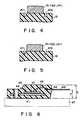
- formation of cracks can also be prevented by forming, in the plastic table along both sides of the outer lead 151, trenches 201 and 202 as shown in Fig. 4 or trenches 211 and 212 as shown in Fig. 5.
- this structure of the present invention can be directly applied to a plastic molded type semiconductor device constituting a rectifying device having poor heat dissipation characteristics, an integrated circuit element, or the like.
Landscapes
- Structures Or Materials For Encapsulating Or Coating Semiconductor Devices Or Solid State Devices (AREA)
- Cooling Or The Like Of Semiconductors Or Solid State Devices (AREA)
Applications Claiming Priority (2)
| Application Number | Priority Date | Filing Date | Title |
|---|---|---|---|
| JP1247268A JPH03108744A (ja) | 1989-09-22 | 1989-09-22 | 樹脂封止型半導体装置 |
| JP247268/89 | 1989-09-22 |
Publications (3)
| Publication Number | Publication Date |
|---|---|
| EP0418891A2 true EP0418891A2 (fr) | 1991-03-27 |
| EP0418891A3 EP0418891A3 (en) | 1992-04-08 |
| EP0418891B1 EP0418891B1 (fr) | 1996-07-10 |
Family
ID=17160946
Family Applications (1)
| Application Number | Title | Priority Date | Filing Date |
|---|---|---|---|
| EP90118124A Expired - Lifetime EP0418891B1 (fr) | 1989-09-22 | 1990-09-20 | Dispositif semi-conducteur de puissance à encapsulation en plastique |
Country Status (5)
| Country | Link |
|---|---|
| US (1) | US5063434A (fr) |
| EP (1) | EP0418891B1 (fr) |
| JP (1) | JPH03108744A (fr) |
| KR (1) | KR930004247B1 (fr) |
| DE (1) | DE69027724T2 (fr) |
Cited By (5)
| Publication number | Priority date | Publication date | Assignee | Title |
|---|---|---|---|---|
| EP0508615A1 (fr) * | 1991-04-10 | 1992-10-14 | Caddock Electronics, Inc. | Résistance en couche |
| EP0511702A3 (en) * | 1991-04-26 | 1993-06-09 | Consorzio Per La Ricerca Sulla Microelettronica Nel Mezzogiorno | Semiconductor device encapsulated in resin and completely insulated for high voltages |
| EP0637081A3 (fr) * | 1993-07-27 | 1996-03-20 | Siemens Ag | Micro détecteur avec fiches de connexions. |
| KR20150089177A (ko) * | 2014-01-27 | 2015-08-05 | 삼성전자주식회사 | 반도체 소자 |
| US12476158B2 (en) | 2021-03-11 | 2025-11-18 | Fuji Electric Co., Ltd. | Semiconductor module and manufacturing method of semiconductor module |
Families Citing this family (11)
| Publication number | Priority date | Publication date | Assignee | Title |
|---|---|---|---|---|
| JP2580840B2 (ja) * | 1990-05-22 | 1997-02-12 | 日本電気株式会社 | 半導体装置用パッケージ |
| EP0468379B1 (fr) * | 1990-07-21 | 1999-11-17 | Mitsui Chemicals, Inc. | Dispositif semi-conducteur comprenant un empaquetage |
| IT1252624B (it) * | 1991-12-05 | 1995-06-19 | Cons Ric Microelettronica | Dispositivo semiconduttore incapsulato in resina e elettricamente isolato di migliorate caratteristiche di isolamento,e relativo processo di fabbricazione |
| JP3406753B2 (ja) * | 1995-11-30 | 2003-05-12 | 三菱電機株式会社 | 半導体装置および半導体モジュール |
| US6372526B1 (en) * | 1998-04-06 | 2002-04-16 | Semiconductor Components Industries Llc | Method of manufacturing semiconductor components |
| US6262512B1 (en) * | 1999-11-08 | 2001-07-17 | Jds Uniphase Inc. | Thermally actuated microelectromechanical systems including thermal isolation structures |
| US6791172B2 (en) * | 2001-04-25 | 2004-09-14 | General Semiconductor Of Taiwan, Ltd. | Power semiconductor device manufactured using a chip-size package |
| US7061077B2 (en) * | 2002-08-30 | 2006-06-13 | Fairchild Semiconductor Corporation | Substrate based unmolded package including lead frame structure and semiconductor die |
| KR101391925B1 (ko) * | 2007-02-28 | 2014-05-07 | 페어차일드코리아반도체 주식회사 | 반도체 패키지 및 이를 제조하기 위한 반도체 패키지 금형 |
| DE102007051870A1 (de) * | 2007-10-30 | 2009-05-07 | Robert Bosch Gmbh | Modulgehäuse und Verfahren zur Herstellung eines Modulgehäuses |
| CN113261095B (zh) * | 2019-01-18 | 2024-11-26 | 三菱电机株式会社 | 半导体装置、半导体装置的制造方法及电力转换装置 |
Family Cites Families (4)
| Publication number | Priority date | Publication date | Assignee | Title |
|---|---|---|---|---|
| JPS564255A (en) * | 1979-06-25 | 1981-01-17 | Hitachi Ltd | Semiconductor device sealed up with resin |
| JPS58209147A (ja) * | 1982-05-31 | 1983-12-06 | Toshiba Corp | 樹脂封止型半導体装置 |
| JPS6116556A (ja) * | 1984-07-03 | 1986-01-24 | Matsushita Electronics Corp | 樹脂封止型半導体装置 |
| JPS63107152A (ja) * | 1986-10-24 | 1988-05-12 | Hitachi Ltd | 樹脂封止型電子部品 |
-
1989
- 1989-09-22 JP JP1247268A patent/JPH03108744A/ja active Pending
-
1990
- 1990-09-18 US US07/584,043 patent/US5063434A/en not_active Expired - Lifetime
- 1990-09-20 DE DE69027724T patent/DE69027724T2/de not_active Expired - Fee Related
- 1990-09-20 EP EP90118124A patent/EP0418891B1/fr not_active Expired - Lifetime
- 1990-09-21 KR KR1019900014985A patent/KR930004247B1/ko not_active Expired - Fee Related
Cited By (10)
| Publication number | Priority date | Publication date | Assignee | Title |
|---|---|---|---|---|
| EP0508615A1 (fr) * | 1991-04-10 | 1992-10-14 | Caddock Electronics, Inc. | Résistance en couche |
| US5291178A (en) * | 1991-04-10 | 1994-03-01 | Caddock Electronics, Inc. | Film-type resistor assembly with full encapsulation except at the bottom surface |
| US6320258B1 (en) | 1991-04-23 | 2001-11-20 | Consorzio Per La Ricerca Sulla Microelectronica Nel Mezzogiorno | Semiconductor device having alternating electrically insulative coated leads |
| EP0511702A3 (en) * | 1991-04-26 | 1993-06-09 | Consorzio Per La Ricerca Sulla Microelettronica Nel Mezzogiorno | Semiconductor device encapsulated in resin and completely insulated for high voltages |
| EP0637081A3 (fr) * | 1993-07-27 | 1996-03-20 | Siemens Ag | Micro détecteur avec fiches de connexions. |
| KR20150089177A (ko) * | 2014-01-27 | 2015-08-05 | 삼성전자주식회사 | 반도체 소자 |
| EP2899754A3 (fr) * | 2014-01-27 | 2015-10-07 | Samsung Electronics Co., Ltd | Dispositif semi-conducteur |
| US9711435B2 (en) | 2014-01-27 | 2017-07-18 | Samsung Electronics Co., Ltd. | Semiconductor device |
| KR102192997B1 (ko) | 2014-01-27 | 2020-12-18 | 삼성전자주식회사 | 반도체 소자 |
| US12476158B2 (en) | 2021-03-11 | 2025-11-18 | Fuji Electric Co., Ltd. | Semiconductor module and manufacturing method of semiconductor module |
Also Published As
| Publication number | Publication date |
|---|---|
| KR910007116A (ko) | 1991-04-30 |
| EP0418891B1 (fr) | 1996-07-10 |
| JPH03108744A (ja) | 1991-05-08 |
| DE69027724D1 (de) | 1996-08-14 |
| US5063434A (en) | 1991-11-05 |
| EP0418891A3 (en) | 1992-04-08 |
| KR930004247B1 (ko) | 1993-05-22 |
| DE69027724T2 (de) | 1996-12-05 |
Similar Documents
| Publication | Publication Date | Title |
|---|---|---|
| US7501700B2 (en) | Semiconductor power module having an electrically insulating heat sink and method of manufacturing the same | |
| US6476481B2 (en) | High current capacity semiconductor device package and lead frame with large area connection posts and modified outline | |
| US7642640B2 (en) | Semiconductor device and manufacturing process thereof | |
| US5703399A (en) | Semiconductor power module | |
| US7671382B2 (en) | Semiconductor device with thermoplastic resin to reduce warpage | |
| KR930002804B1 (ko) | 수지밀봉형 반도체장치 | |
| EP0247775B1 (fr) | Empaquetage pour semi-conducteurs ayant des connexions entrée/sortie à haute densité | |
| JP2801534B2 (ja) | パワー半導体モジュールおよびそれに使用する絶縁金属基板 | |
| US5747876A (en) | Semiconductor device and semiconductor module | |
| EP0418891B1 (fr) | Dispositif semi-conducteur de puissance à encapsulation en plastique | |
| EP0532244B1 (fr) | Dispositif semi-conducteur | |
| CN1086373A (zh) | 电源模块 | |
| CN111883490A (zh) | 具有用于顶侧冷却的多级传导夹的半导体封装 | |
| EP0777272A2 (fr) | Dispositif semi-conducteur | |
| KR19980032479A (ko) | 표면 설치 to-220 패키지 및 그의 제조 공정 | |
| JP6760127B2 (ja) | 半導体装置、半導体装置の製造方法 | |
| CN121712087A (zh) | 半导体装置 | |
| US5517058A (en) | Semiconductor package and method with vertically extended electrode leads | |
| JPH06302734A (ja) | 電力用半導体モジュール | |
| CN120751756B (zh) | 半导体装置 | |
| CN219085965U (zh) | 表面贴装金属散热块的半导体电路组件和散热组件 | |
| US20230343770A1 (en) | Semiconductor module | |
| JP2512289B2 (ja) | 樹脂封止型半導体装置 | |
| EP0181975B1 (fr) | Dispositif semi-conducteur comprenant un corps de support | |
| JP2713141B2 (ja) | 半導体装置 |
Legal Events
| Date | Code | Title | Description |
|---|---|---|---|
| PUAI | Public reference made under article 153(3) epc to a published international application that has entered the european phase |
Free format text: ORIGINAL CODE: 0009012 |
|
| 17P | Request for examination filed |
Effective date: 19900920 |
|
| AK | Designated contracting states |
Kind code of ref document: A2 Designated state(s): DE FR GB |
|
| PUAL | Search report despatched |
Free format text: ORIGINAL CODE: 0009013 |
|
| AK | Designated contracting states |
Kind code of ref document: A3 Designated state(s): DE FR GB |
|
| 17Q | First examination report despatched |
Effective date: 19940720 |
|
| GRAH | Despatch of communication of intention to grant a patent |
Free format text: ORIGINAL CODE: EPIDOS IGRA |
|
| GRAA | (expected) grant |
Free format text: ORIGINAL CODE: 0009210 |
|
| AK | Designated contracting states |
Kind code of ref document: B1 Designated state(s): DE FR GB |
|
| GRAH | Despatch of communication of intention to grant a patent |
Free format text: ORIGINAL CODE: EPIDOS IGRA |
|
| REF | Corresponds to: |
Ref document number: 69027724 Country of ref document: DE Date of ref document: 19960814 |
|
| ET | Fr: translation filed | ||
| PLBE | No opposition filed within time limit |
Free format text: ORIGINAL CODE: 0009261 |
|
| STAA | Information on the status of an ep patent application or granted ep patent |
Free format text: STATUS: NO OPPOSITION FILED WITHIN TIME LIMIT |
|
| 26N | No opposition filed | ||
| REG | Reference to a national code |
Ref country code: GB Ref legal event code: 746 Effective date: 19981103 |
|
| REG | Reference to a national code |
Ref country code: FR Ref legal event code: D6 |
|
| REG | Reference to a national code |
Ref country code: GB Ref legal event code: IF02 |
|
| PGFP | Annual fee paid to national office [announced via postgrant information from national office to epo] |
Ref country code: DE Payment date: 20070913 Year of fee payment: 18 |
|
| PGFP | Annual fee paid to national office [announced via postgrant information from national office to epo] |
Ref country code: GB Payment date: 20070919 Year of fee payment: 18 |
|
| PGFP | Annual fee paid to national office [announced via postgrant information from national office to epo] |
Ref country code: FR Payment date: 20070914 Year of fee payment: 18 |
|
| GBPC | Gb: european patent ceased through non-payment of renewal fee |
Effective date: 20080920 |
|
| REG | Reference to a national code |
Ref country code: FR Ref legal event code: ST Effective date: 20090529 |
|
| PG25 | Lapsed in a contracting state [announced via postgrant information from national office to epo] |
Ref country code: DE Free format text: LAPSE BECAUSE OF NON-PAYMENT OF DUE FEES Effective date: 20090401 |
|
| PG25 | Lapsed in a contracting state [announced via postgrant information from national office to epo] |
Ref country code: FR Free format text: LAPSE BECAUSE OF NON-PAYMENT OF DUE FEES Effective date: 20080930 |
|
| PG25 | Lapsed in a contracting state [announced via postgrant information from national office to epo] |
Ref country code: GB Free format text: LAPSE BECAUSE OF NON-PAYMENT OF DUE FEES Effective date: 20080920 |