EP0419930B1 - Methode zur Verhinderung einer Partikel-Verunreinigung - Google Patents
Methode zur Verhinderung einer Partikel-Verunreinigung Download PDFInfo
- Publication number
- EP0419930B1 EP0419930B1 EP90117459A EP90117459A EP0419930B1 EP 0419930 B1 EP0419930 B1 EP 0419930B1 EP 90117459 A EP90117459 A EP 90117459A EP 90117459 A EP90117459 A EP 90117459A EP 0419930 B1 EP0419930 B1 EP 0419930B1
- Authority
- EP
- European Patent Office
- Prior art keywords
- plasma
- wafer
- particulates
- reactor
- chamber
- Prior art date
- Legal status (The legal status is an assumption and is not a legal conclusion. Google has not performed a legal analysis and makes no representation as to the accuracy of the status listed.)
- Expired - Lifetime
Links
Images


Classifications
-
- H—ELECTRICITY
- H10—SEMICONDUCTOR DEVICES; ELECTRIC SOLID-STATE DEVICES NOT OTHERWISE PROVIDED FOR
- H10P—GENERIC PROCESSES OR APPARATUS FOR THE MANUFACTURE OR TREATMENT OF DEVICES COVERED BY CLASS H10
- H10P14/00—Formation of materials, e.g. in the shape of layers or pillars
- H10P14/60—Formation of materials, e.g. in the shape of layers or pillars of insulating materials
- H10P14/65—Formation of materials, e.g. in the shape of layers or pillars of insulating materials characterised by treatments performed before or after the formation of the materials
- H10P14/6516—Formation of materials, e.g. in the shape of layers or pillars of insulating materials characterised by treatments performed before or after the formation of the materials of treatments performed after formation of the materials
- H10P14/6529—Formation of materials, e.g. in the shape of layers or pillars of insulating materials characterised by treatments performed before or after the formation of the materials of treatments performed after formation of the materials by exposure to a gas or vapour
- H10P14/6532—Formation of materials, e.g. in the shape of layers or pillars of insulating materials characterised by treatments performed before or after the formation of the materials of treatments performed after formation of the materials by exposure to a gas or vapour by exposure to a plasma
-
- H—ELECTRICITY
- H01—ELECTRIC ELEMENTS
- H01J—ELECTRIC DISCHARGE TUBES OR DISCHARGE LAMPS
- H01J37/00—Discharge tubes with provision for introducing objects or material to be exposed to the discharge, e.g. for the purpose of examination or processing thereof
- H01J37/32—Gas-filled discharge tubes
- H01J37/32431—Constructional details of the reactor
-
- C—CHEMISTRY; METALLURGY
- C23—COATING METALLIC MATERIAL; COATING MATERIAL WITH METALLIC MATERIAL; CHEMICAL SURFACE TREATMENT; DIFFUSION TREATMENT OF METALLIC MATERIAL; COATING BY VACUUM EVAPORATION, BY SPUTTERING, BY ION IMPLANTATION OR BY CHEMICAL VAPOUR DEPOSITION, IN GENERAL; INHIBITING CORROSION OF METALLIC MATERIAL OR INCRUSTATION IN GENERAL
- C23C—COATING METALLIC MATERIAL; COATING MATERIAL WITH METALLIC MATERIAL; SURFACE TREATMENT OF METALLIC MATERIAL BY DIFFUSION INTO THE SURFACE, BY CHEMICAL CONVERSION OR SUBSTITUTION; COATING BY VACUUM EVAPORATION, BY SPUTTERING, BY ION IMPLANTATION OR BY CHEMICAL VAPOUR DEPOSITION, IN GENERAL
- C23C16/00—Chemical coating by decomposition of gaseous compounds, without leaving reaction products of surface material in the coating, i.e. chemical vapour deposition [CVD] processes
- C23C16/44—Chemical coating by decomposition of gaseous compounds, without leaving reaction products of surface material in the coating, i.e. chemical vapour deposition [CVD] processes characterised by the method of coating
- C23C16/4401—Means for minimising impurities, e.g. dust, moisture or residual gas, in the reaction chamber
-
- C—CHEMISTRY; METALLURGY
- C23—COATING METALLIC MATERIAL; COATING MATERIAL WITH METALLIC MATERIAL; CHEMICAL SURFACE TREATMENT; DIFFUSION TREATMENT OF METALLIC MATERIAL; COATING BY VACUUM EVAPORATION, BY SPUTTERING, BY ION IMPLANTATION OR BY CHEMICAL VAPOUR DEPOSITION, IN GENERAL; INHIBITING CORROSION OF METALLIC MATERIAL OR INCRUSTATION IN GENERAL
- C23C—COATING METALLIC MATERIAL; COATING MATERIAL WITH METALLIC MATERIAL; SURFACE TREATMENT OF METALLIC MATERIAL BY DIFFUSION INTO THE SURFACE, BY CHEMICAL CONVERSION OR SUBSTITUTION; COATING BY VACUUM EVAPORATION, BY SPUTTERING, BY ION IMPLANTATION OR BY CHEMICAL VAPOUR DEPOSITION, IN GENERAL
- C23C16/00—Chemical coating by decomposition of gaseous compounds, without leaving reaction products of surface material in the coating, i.e. chemical vapour deposition [CVD] processes
- C23C16/44—Chemical coating by decomposition of gaseous compounds, without leaving reaction products of surface material in the coating, i.e. chemical vapour deposition [CVD] processes characterised by the method of coating
- C23C16/54—Apparatus specially adapted for continuous coating
-
- H—ELECTRICITY
- H10—SEMICONDUCTOR DEVICES; ELECTRIC SOLID-STATE DEVICES NOT OTHERWISE PROVIDED FOR
- H10P—GENERIC PROCESSES OR APPARATUS FOR THE MANUFACTURE OR TREATMENT OF DEVICES COVERED BY CLASS H10
- H10P70/00—Cleaning of wafers, substrates or parts of devices
- H10P70/10—Cleaning before device manufacture, i.e. Begin-Of-Line process
- H10P70/12—Cleaning before device manufacture, i.e. Begin-Of-Line process by dry cleaning only
- H10P70/125—Cleaning before device manufacture, i.e. Begin-Of-Line process by dry cleaning only with gaseous HF
-
- H—ELECTRICITY
- H10—SEMICONDUCTOR DEVICES; ELECTRIC SOLID-STATE DEVICES NOT OTHERWISE PROVIDED FOR
- H10P—GENERIC PROCESSES OR APPARATUS FOR THE MANUFACTURE OR TREATMENT OF DEVICES COVERED BY CLASS H10
- H10P70/00—Cleaning of wafers, substrates or parts of devices
- H10P70/20—Cleaning during device manufacture
-
- H—ELECTRICITY
- H01—ELECTRIC ELEMENTS
- H01J—ELECTRIC DISCHARGE TUBES OR DISCHARGE LAMPS
- H01J2237/00—Discharge tubes exposing object to beam, e.g. for analysis treatment, etching, imaging
- H01J2237/02—Details
- H01J2237/022—Avoiding or removing foreign or contaminating particles, debris or deposits on sample or tube
Definitions
- This invention relates in general to particulate contamination in integrated circuit (IC) processing and relates more particularly to a plasma reactor design and process that greatly reduces the particulate contamination of wafers during etching of or deposit of thin films on a wafer within such a plasma reactor.
- IC integrated circuit
- Integrated circuit processing technology is continuously concerned with reducing the feature size of circuits to increase the amount of circuitry that can be packed onto an integrated circuit of a given size and to increase the speed of operation by reducing the distance that signals need to travel within such circuits.
- feature size has decreased and as circuit complexity has increased, the effect of particulate contamination on process yields has become increasingly important. Particulates of diameter even several times smaller than the feature size of a component can cause failure of the IC if a particle was present at a critical location in the IC during a plasma process step.
- particulates on yield is particularly critical for the submicron minimum feature size circuits available today because particulates as small as a fraction of a micron can make a circuit inoperable.
- the numbers of such particles has been found to increase rapidly with decreasing size. This problem is particularly acute for large area ICs such as microprocessors and ⁇ 4 megabit memories because such ICs have an increased area over which a critical defect can occur.
- a particulate incorporated into one level of an IC can affect not only the circuitry on that level, but can also affect circuity on other levels.
- a defect in an embedded level of an IC can propagate through overlying layers, distorting the topography and thus disrupting operation of those circuit elements. For these reasons it is important to minimize the amount of particulates that come into contact with a wafer immediately before and during processing.
- Plasma reactors can be used in a number of different phases of IC processing. These uses of plasma reactors include plasma etching, reactive ion etching and plasma enhanced chemical vapor deposition. Airborne particulates within a plasma reactor can settle onto a wafer, thereby potentially interfering with subsequently produced IC circuitry.
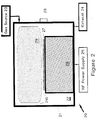
- Figure 1 illustrates the relative size of some common airborne particulates (see, for example, chapter 7 of the text by Peter Van Zant entitled Microchip Fabrication, published by Semiconductor Services, San Jose, California, 1985). Expensive, intricate clean rooms and clean room procedures are utilized to significantly reduce the amount of airborne particulates to which a wafer is exposed during IC fabrication.
- Figure 3 illustrates a wafer handling system 30 that allows a robot 31 to supply wafers to any of a plurality of IC processing chambers.
- This system enables wafers 32 to be exchanged between a wafer cassette elevator 33 and any of the chambers 34-37 without breaking vacuum in these chambers.
- Robot 31 includes an extensible arm 38 that can extend a wafer blade 38 radially into any of chambers 33-37.
- Arm 38 is mounted on a rotatable table 310 that enables extensible arm to be directed at any selected one of chambers 33-37. This enables the chambers to be carefully cleaned and purged before wafers are introduced for processing.
- a plasma reactor design is presented that prevents most of the airborne particulates within a plasma reactor chamber from depositing on a wafer within the chamber.
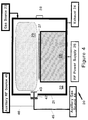
- a typical existing plasma reactor is illustrated in Figure 2.
- a plasma consists of two qualitatively different regions: the substantially neutral, conductive plasma body and a boundary layer called the plasma sheath.
- the plasma body consists of substantially equal densities of negative and positive charged particles as well as radicals and stable neutral particles.
- the plasma sheath is an electron deficient, poorly conductive region in which the electric field strength is large.
- the plasma sheath forms between the plasma body and any interface such as the walls of the plasma reactor chamber and the rf electrodes.
- Semiconductor process plasmas are usually produced by a radio frequency (rf) field that couples energy into free electrons within the chamber, imparting sufficient energy to many of these electrons such that ions can be produced through collisions of these electrons with gas molecules.
- rf radio frequency
- the walls of the reactor chamber are metal (though often coated with thin insulating layers) so that they function as one of the rf electrodes.
- the powered rf electrode often also functions as a pedestal on which a wafer is placed for processing. This has the benefit of generating the strongest rf electric field and ion bombardment in the neighborhood of and on the wafer.
- the electrons are on the order of thousands to hundreds of thousands of times lighter than the plasma ions, they experience an equally greater acceleration than the ions and therefore acquire from the rf field kinetic energies that are somewhat greater than those acquired by the ions.
- the effect of this is that the energy from the rf field is strongly coupled into electron kinetic energy and only very weakly coupled into ion kinetic energy.
- collisions between the high energy (also referred to as high temperature) electrons and the ions does not transfer much of the electron energy to the ions.
- the effect of this is that the electrons acquire a temperature that is typically on the order of 1-5 ev and the other particles in the plasma remain substantially at the temperature of the walls of the plasma reactor chamber or up to a few hundred degrees Centigrade hotter.
- the electrons are much more mobile than the ions, they initially strike the walls of the reactor chamber at a greater rate than do the ions.
- the effect of this is that the plasma body becomes slightly electron deficient while the boundary layer sheath becomes substantially electron deficient and thus positively charged at its interface with the electrodes.
- This net positive charge of the plasma body and boundary layer results in a plasma body electrical potential (usually called the "plasma potential") on the order of several times the electron mean kinetic energy divided by the electron charge.
- the potential in the bulk of the plasma is nearly constant while the largest part of the potential variation is across the sheath.
- this sheath potential is also dependent on various parameters including the area of the reactor chamber wall, the area of the powered electrode, the pressure in the reactor chamber and the rf power input (see, for example, J. Coburn and E. Kay, J. Appl. Phys., 43 , p. 4965 (1972).
- the resulting time average sheath potential is approximately the sum of its value for a dc plasma, as described above, plus the amplitude of the rf component of the plasma potential.
- a non-electronegative plasma e.g., a plasma in which the concentration of negative ions does not greatly exceed that of electrons
- the high speed free electrons within the plasma quickly charge particulates negative within the plasma body.
- the plasma body is positively charged with respect to surfaces in ac contact with ground
- the dc electric field across the plasma sheath between the plasma body and the powered electrode acts to hold these charged particulates away from both the powered electrode and the wafer located on the powered electrode.
- This dc electric field across the plasma sheath exists at any surface within the chamber, including the wafer surface. When the plasma is turned off, this electric field vanishes, thereby enabling the particulates to settle onto the wafer.
- a plasma is maintained within the reactor chamber at all times that a wafer is within the chamber, including those times during which a wafer is being transferred into or out of the chamber.
- This may either be the active processing plasma or an auxiliary or supplemental plasma of moderate or low power produced either by the power supply for the process plasma or by an independent source.
- the plasma density produced by this auxiliary plasma source is typically reduced from the level during the active process to a level just sufficient to prevent the particulates from settling onto the wafer.
- the gas supply during this period is substantially nonhalogenated in order to avoid both processing and an electronegative character of the plasma. Further, there may be an r.f.
- This level is typically significantly less than the level that occurs during wafer processing in the plasma reactor and avoids processing of the wafer during the periods of transfer into and out of the reactor chamber.
- both the charge on the particulates and the strength of the dc electric field at the wafer decrease. Therefore, the force on the particulates, which is the product of these two terms, decreases even faster than either of these terms.
- this lower density plasma for particulate protection must have a minimum density of electrons of order or greater than 108 cm ⁇ 3.
- the plasma is preferably produced by an auxiliary plasma source located away from the wafer pedestal to further minimize processing of the wafer during these periods.
- Any plasma source can be used, including an auxiliary rf electrode, a hollow cathode or a microwave plasma cavity.
- the plasma reactor chamber should contain a wafer transfer valve with minimum area to reduce plasma flow into non-processing chambers during the wafer transfer.
- Figure 1 illustrates the relative size of some common airborne particulates.
- Figure 2 illustrates a typical plasma reactor.
- Figure 3 illustrates a wafer handling system that allows a robot to supply wafers to a plurality of IC processing chambers.
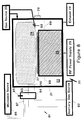
- Figure 4 illustrates a preferred embodiment of the invention utilizing an auxiliary rf plasma source.
- Figure 5 illustrates in greater detail a simple choice of the auxiliary rf plasma source.
- Figure 6 shows the timing of activation of the primary and secondary plasma sources.
- Figure 7 shows the electrical equivalent circuit of a plasma reactor.
- Figure 8 illustrates an alternate embodiment of the invention utilizing a microwave plasma source as the auxiliary plasma source.
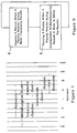
- Figure 9 outlines a method of keeping particulates away from a wafer in a plasma reactor.
- Figure 9 outlines a method of keeping particulates away from a wafer in a plasma reactor.
- a plasma of reduced intensity is produced to keep particulates away from the wafer while avoiding significant processing of the wafer.
- FIG. 4 illustrates a conventional plasma reactor 20 to which has been added an auxiliary plasma source, such as auxiliary rf source 41, and an auxiliary gas source 44 to assist use of this reactor to practice the process of Figure 9.
- This reactor includes an aluminum wall 21 that encloses a plasma reactor chamber 22. Wall 21 is grounded and functions as one of the plasma electrodes. Gases are supplied to chamber 22 from a gas source 23 and are exhausted by an exhaust system 24 that typically actively pumps gases out of the reactor to maintain a low pressure suitable for a plasma process.
- An rf power supply 25 provides power to a second (powered) electrode 26 to generate a plasma within chamber 22.
- gas source 23 could provide gases to plasma chamber 22 during the wafer transfer periods, these gases are preferably provided by an auxiliary gas source 44.
- auxiliary gas source 44 provides gasses to chamber 22 through a metallic feed that terminates in a set of holes in an electrode 43.
- RF power is provided to electrode 43 via a conductor 46 connecting auxiliary rf source 41 to gas feed 45 which is conductively coupled to electrode 43.
- Powered electrode 26 also functions as a pedestal on which a wafer 27 is supported during processing within the reactor chamber. This has the advantage of locating the wafer at the location of strongest rf field, thereby enhancing the density of the plasma at the wafer.
- the wafer is transferred into and out of reactor chamber 22 through a port 28 such as the slit valve presented in U.S. patent 4,785,962 entitled Vacuum Chamber Slit Valve, issued to Massato Toshima on November 22, 1988.
- This slit valve has the advantages of effectively sealing chamber 22 during processing and of presenting a minimal area opening through which wafers are transferred into and out of chamber 22. This minimizes leakage of reactor gases through port 28 during wafer transfer into or out of chamber 22.
- the resulting rf electric field in the chamber couples energy into free electrons which then ionize halogenated and other gases within the chamber, thereby producing a plasma body 29 surrounded by a plasma sheath 210.
- the plasma sheath exists between the plasma body and all reactor chamber boundaries adjacent to the plasma body because of the higher mobility of the plasma electrons.
- the plasma is first turned on, for a few microseconds, more electrons hit electrode 21 and wafer 27 than do ions such that the plasma becomes positively charged relative to both electrodes. This results in an electric field across the plasma sheath from the plasma body to both electrodes which is directed such as to accelerate positive ions outward from the plasma body and keep negative particles in.
- the dc component of the voltage of the plasma adjusts until a steady state is reached in which most electrons are repelled at the sheath such that zero dc electric current travels from the plasma's body 29 to ground.
- Actual values of the voltages can be determined from an equivalent circuit of this electrical structure discussed below.
- the rf component of the electric field is too small to have any significant effect on repelling these particulates away from the wafer.
- the rf field induces an increase in the dc electric field which helps in repelling particulates from surfaces, including the wafer.
- the dc voltage V p of the plasma is approximately equal to kT e ⁇ ln[ ⁇ m i /2 ⁇ m e ⁇ 1/2 ]/e
- T e is the temperature of the plasma electrons
- m i is the mass of a typical plasma ion
- m e is the mass of an electron
- e is the charge of an electron.
- V p is on the order of 5kT e /e.
- the dc value of its potential rises to roughly the sum of the dc value plus the rf amplitude.
- the level of rf power and gas pressure determine T e .
- RF power supply 25 is typically capacitively coupled to powered electrode 26 so that this electrode's dc potential can float relative to grounded wall 21. If the electrode has smaller exposed area than the walls, the electrode floats to a potential nearly as negative as the amplitude of its rf potential (see, for example, the reference by J. Coburn cited above). This reduces sputtering of chamber wall 21 by reducing the sheath potential at the boundary between the plasma body and the chamber wall.
- the plasma could be maintained during periods of wafer transfer by continuing to pump rf energy from rf power supply 25 into the plasma through electrode 26.
- the rf power would be reduced during such wafer transfer periods to the minimal level that substantially keeps particulates from settling onto the wafer. This would minimize any processing of the wafer during such transfer periods while preventing particulates from settling onto the wafer. This would, however, still cause the highest energy ions to hit the wafer, as well as the bare electrode.
- this alternate plasma source consists of auxiliary rf source 41 which couples rf power into auxiliary power electrode assembly 42.
- rf source 41 can be omitted and replaced by switchable power from rf power supply 25.
- Electrode 43 There are many known ways to couple power from an rf source to a powered electrode.
- a particularly simple embodiment of electrode 43 is presented in Figure 5.
- Hollow gas feed 45 enters chamber 22 through an insulating power feed 51 consisting of a ceramic end section 52 and a sidewall 53. This gas feed ejects gas into chamber 22 through holes in electrode 43.
- the diameter and length of electrode 43 are such that its surface area is less than that of the main electrode and therefore it produces a modest rf component of the plasma potential. This reduces sputtering of the walls and wafer during transfer.
- FIG. 7 shows the equivalent circuit of the electrical discharge in the plasma reactor.
- the positive electric charge in the sheath region between the plasma body and the electrode surfaces is capacitive charge storage that can be modeled as a capacitance C s1 between the powered electrode and the plasma body. There is also a capacitance C s2 between the walls and the plasma body.
- the plasma itself is essentially resistive for rf frequencies below the "plasma frequency”.
- the low conductivity of the sheath introduces a high resistive component R s1 in parallel with C s1 and a high resistive component R s2 in parallel with C s2 .
- the high conductivity of the plasma means that the plasma functions as a low resistive component R p .
- a blocking capacitor 72 between powered electrode 26 and the power supply enables the dc potential of powered electrode 26 to float.
- diodes D1 and D2 the effects of diodes D1 and D2, and of resistances R s1 and R s2 can be ignored.
- capacitors C, C s1 and C s2 function as a capacitive divider.
- the auxiliary electrode should have a diameter on the order of five centimeters such that with a power input on the order of 100 Watts the resulting plasma, which has an electron density of order 109 cm ⁇ 3, has an rf potential less than 40 volts.
- Figure 6 is a timing diagram that plots as a function of time the power provided by rf sources 25 (shown as solid lines 61 and 63) and 41 (shown as dashed line 62). This diagram illustrates that power is provided at all times while a wafer is in the chamber. This assures that plasma is present in the chamber at all times. The wafer transfer occurs during the interval T when no power is supplied to the main processing electrode 26. It should be noted that the amount of power from rf power source 41 will have a peak value that is usually substantially less than the peak value of power from rf power source 25. The amount of power required from auxiliary rf source 41 is determined by the geometry of the plasma reactor and the maximum size of particulates that are to be electrostatically repelled away from the wafer.
- the current and voltage of rf power supply 25 are typically selected to produce a plasma body charge density on the order of 109 - 1011 free electrons per cubic centimeter.
- the pressure in the reactor chamber is typically on the order of 1.3 - 1.3.103 Pa (10 ⁇ 2 - 10 Torr). With these choices of parameters, the dc plasma potential is typically on the order of 10-100 volts.
- particulate size on minimum power 62 from the auxiliary plasma source can be seen as follows.
- particulates typically have a density on the order of 3 grams per cubic centimeter so that a particulate of diameter on the order of 1 micron weighs on the order of 10 ⁇ 14 Newtons. If this particulate is charged, with 1000 electrons net charge, then the electric field at powered electrode 26 should exceed 10 ⁇ 14 Newtons/1.6 ⁇ 10 ⁇ 16 Coulombs which means a field of 0.60 volts/cm to repel the particulate against gravity.
- Typical chamber volumes range from 1 liter to as much as 10's of liters.
- the magnitude of the electric field at the sheath above the wafer is on the order of 5kT e /e ⁇ D where ⁇ D is the Debye length which is equal to [ ⁇ o kT e /ne2] 1/2 and which is less than 1 mm at a density of 109 free electrons per cm3.
- This field is on the order of 10-100 volts/cm which easily satisfies the field requirements to keep particulates away from the wafer.
- the dc sheath voltage above electrode 26 should be not much more than about 25 volts to avoid significant sputtering of the thin films on the surface of the wafer during the wafer exchange intervals.
- the peak rf power supplied to electrode assembly 42 should be in the range from ten to a few hundred Watts. Since the particulate charge (and hence the electric force) increases linearly with particulate diameter and its weight increases as particulate diameter to the third power, this range of rf power will prevent particulates on the order of several microns or smaller from depositing onto the wafer.
- the dc field between the electrodes and the plasma repels these negatively charged particulates away from the wafer. It was also indicated that this negative charge on the particulates arises because the electrons are so much more mobile than are the plasma ions. Implicitly, this assumes that the plasma contains a sufficient number of electrons that indeed the particulates become negatively charged. This will usually be the case, but there are some reactant gases that are sufficiently electronegative that this will not be the case at modest power levels.
- the processing gases should be purged from the plasma reactor chamber as quickly as possible and replaced with a nonhalogcnated feed gas such that the particulates become negatively charged during the wafer exchange intervals.
- these wafer transfer reactants are purged from the chamber and replaced by suitable process reactants.
- Typical process gases include CHF3, CF4, SF6, HBr, HCl, Cl2, BCl3, CF2Cl2, SiF4, O2, Ar, and He.
- O2, Ar, He and CF4 have a sufficiently low electronegativity that particulates become strongly negatively charged in low power plasmas containing these reactants.
- Other useful choices are He, N2 and CO2. These examples are not exhaustive, but instead are illustrative of suitable reactant gases for the wafer exchange intervals.
- FIG 8 illustrates an alternate embodiment in which the auxiliary plasma source is a microwave plasma source 81.
- This microwave plasma source consists of a gas source 82 that supplies reactant gases into chamber 22 through a tube 83 such as a quartz tube. This tube passes through a microwave cavity 84 which is tuned by means of a tuning stub 85.
- Microwave power is provided from a microwave source 86 to cavity 84 through a coaxial cable 87. The amount of microwave power should be sufficient to produce a plasma such that the sheath at electrode 26 has an electric field sufficiently strong to repel the particulates. The power requirements are substantially the same as for an rf generated plasma.
- a gas nozzle such as nozzle 88 can be included to provide a lateral flow of gas across the wafer.
- this flow is toward the exhaust 24 so that these particulates are removed from chamber 22.
- Above the exhaust manifold to exhaust system 24 are screens 89 that prevent the plasma from extending too far into the exhaust ports.
- the resulting electric field at these screens can be large enough to prevent these particulates from getting past these screens.
- the hole in the screen should be sufficiently large that the resulting electric field at these holes is low enough that the weight of these particulates and the flow of air through the screen will draw these particulates past these screens.
- a hole size in the screen on the order of several to ten millimeters is sufficient to let most of these particulates pass through these screens.
Landscapes
- Chemical & Material Sciences (AREA)
- Engineering & Computer Science (AREA)
- Physics & Mathematics (AREA)
- Plasma & Fusion (AREA)
- Materials Engineering (AREA)
- Mechanical Engineering (AREA)
- Metallurgy (AREA)
- Organic Chemistry (AREA)
- General Chemical & Material Sciences (AREA)
- Chemical Kinetics & Catalysis (AREA)
- Analytical Chemistry (AREA)
- Chemical Vapour Deposition (AREA)
- ing And Chemical Polishing (AREA)
- Drying Of Semiconductors (AREA)
- Container, Conveyance, Adherence, Positioning, Of Wafer (AREA)
- Physical Or Chemical Processes And Apparatus (AREA)
Claims (13)
- Ein Verfahren zum Rückstoßen von Partikeln von Halbleiterscheiben (27) innerhalb einer Reaktionsgase enthaltenden Plasma-Reaktorkammer (22), wobei das Verfahren die Schritte aufweist:(a) daß dort während Halbleiter-Bearbeitungszeiträumen ein Plasma im Reaktor erzeugt wird; und(b) daß dort während im wesentlichen allen Zeiträumen, innerhalb derer sich eine Halbleiterscheibe (27) in der Reaktorkammer (22) befindet und innerhalb derer im wesentlichen keine Bearbeitung der Halbleiterscheibe (27) auftreten soll, ein im wesentlichen keine Bearbeitung bewirkendes Plasma mit einer niedrigeren Leistung innerhalb des Reaktors erzeugt wird, wodurch Partikel in der Reaktorkammer (22) eine negative Nettoladung bekommen und deshalb von der Halbleiterscheibe (27) zu jeder Zeit zurückgestoßen werden können, zu der sich die Halbleiterscheibe (27) in der Reaktorkammer (22) befindet.
- Ein Verfahren nach Anspruch 1, wobei bei Schritt (b) die Ladungsdichten und Beweglichkeiten der Elektronen und Ionen in der Reaktorkammer (22) derart sind, daß ein elektrisches Gleichfeld, das zum Rückstoßen negativ geladener Partikel von der Halbleiterscheibe (27) weg ausreicht, in einer Plasmahülle genau über der Halbleiterscheibe (27) erzeugt wird, wobei das elektrische Gleichfeld bei der Halbleiterscheibe (27) vorzugsweise wenigstens 1,0 Volt/cm beträgt.
- Ein Verfahren nach Anspruch 1 oder 2, wobei Schritt (b) das Erzeugen eines Plasmas von einer Hilfsplasmaquelle, vorzugsweise einem zum Zuführen dieses Plasmas zu der Reaktorkammer (22) angekoppelten Mikrowellen-Plasmagenerator (83 - 87), oder von einer Hilfselektrode (43) mit angelegter Hochfrequenzleistung in der Reaktorkammer (22) aufweist.
- Ein Verfahren nach irgendeinem vorhergehenden Anspruch, wobei während der Zeiträume der Halbleiterscheiben-Umladung die Reaktionsfähigkeit und die Dichte des Plasmas geringer ist als während der Zeiträume der Halbleiterscheiben-Bearbeitung.
- Ein Verfahren nach irgendeinem vorhergehenden Anspruch, wobei die Halbleiterscheiben (27) während der Zeiträume der Kalbleiterscheiben-Umladung zwischen der Reaktorkammer (22) und dem Außenraum der Reaktorkammer (22) über eine enge Halbleiterscheiben-Umladungsklappe (28) transportiert werden, wodurch der Anteil des aus der Reaktorkammer (22) während einer solchen Umladung ausfließenden Plasmas minimiert wird.
- Ein Verfahren nach irgendeinem vorhergehenden Anspruch, wobei die Reaktionsgase innerhalb der Reaktorkammer (22) während zumindest eines Teils des Schritts (b) durch Reaktionsgase ersetzt werden, die nichthalogeniert und ausreichend elektropositiv sind, damit genügend freie Elektronen in dem Plasma erzeugt werden, so daß Partikel während der Zeiträume der Halbleiterscheiben-Umladung durch das Plasma negativ aufgeladen werden.
- Ein Verfahren nach irgendeinem vorhergehenden Anspruch, wobei die Halbleiterscheibe (27) bei Schritt (b) um einen Winkel aus der Horizontalen weggeschwenkt wird, so daß Schwerkraft und elektromagnetische Abstoßung von Partikeln eine Nettokraft erzeugen, die oberhalb der Hülle ein Driften der Partikel über die Halbleiterscheibe (27) und dann ein Wegdriften von dieser bewirkt, wonach vorzugsweise ein Entfernen der Partikel aus der Reaktorkammer (22), vorzugsweise über geeignet bemessene Löcher in einem Plasma-Begrenzungs-Schirm folgt.
- Ein Verfahren nach irgendeinem vorhergehenden Anspruch, wobei bei Schritt (b) während Zeiträumen der Halbleiterscheiben-Umladung ein Gasfluß über die Halbleiterscheibe (27) gerichtet ist, um Partikel seitlich über die Halbleiterscheibe (27) und dann von dieser weg zu tragen, wonach vorzugsweise ein Entfernen aus der Reaktorkammer (22), vorzugsweise über geeignet bemessene Löcher in einem Plasma-Begrenzungs-Schirm folgt.
- Ein Plasmareaktor (20; 81), aufweisend:
eine Wandung (21), die eine Kammer (22) einschließt;
eine erste Einrichtung (23, 25, 26) zum Erzeugen eines Plasmas, das für eine Bearbeitung einer Halbleiterscheibe (27) in der Reaktorkammer (22) geeignet ist; und
eine zweite Einrichtung (41 - 44; 82 - 87) zum Erzeugen eines im wesentlichen keine Bearbeitung bewirkenden Plasmas innerhalb der Kammer (22), wodurch ein keine Bearbeitung bewirkendes Plasma in der Kammer (22) erzeugt werden kann, um Partikel von einer Halbleiterscheibe innerhalb der Kammer (22) während Zeiträumen zurückzustoßen, in denen keine Bearbeitung der Halbleiterscheibe (27) gewünscht ist. - Ein Reaktor (20; 81) nach Anspruch 9, wobei die zweite Einrichtung zum Erzeugen eines im wesentlichen keine Bearbeitung bewirkenden Plasmas eine Hilfselektrode (43), die mit einer elektrischen Leistungsquelle (41; 25) verbunden ist, oder eine Mikrowellen-Plasmaquelle (83 - 87) aufweist.
- Ein Reaktor (81) nach Anspruch 9 oder 10, der ferner eine Einrichtung zum Richten eines Gasflusses über die Halbleiterscheibe (27), vorzugsweise in der Form einer mit einer Gasquelle (23) verbundenen Düse (88) aufweist.
- Ein Reaktor (81) nach einem der Ansprüche 9 bis 11, der ferner eine Einrichtung (82) zum Ersetzen von Reaktionsgasen während Zeiträumen, in denen keine Bearbeitung erfolgt, durch ein Hilfsgas aufweist, das zum Aufrechterhalten eines Plasmas mit niedriger Stärke geeignet ist, das zum Zurückstoßen von Partikeln von der Halbleiterscheibe (27) ausreicht, wobei das Hilfsgas vorzugsweise nichthalogeniert und ausreichend elektropositiv ist, damit Partikel innerhalb der Reaktorkammer (22) negativ aufgeladen werden.
- Ein Reaktor (81) nach einem der Ansprüche 9 bis 12, der ferner einen Satz von Schirmen (89) innerhalb einer Auslaßöffnung zum Verhindern, daß sich das Plasma über die Schirme (89) hinaus erstreckt, aufweist, wobei die Schirme Öffnungen von zumindest 4 mm Durchmesser aufweisen, wodurch jedes beliebige elektrische Feld an solchen Öffnungen ausreichend schwach ist, daß Partikel durch diese Öffnungen fallen können.
Applications Claiming Priority (2)
| Application Number | Priority Date | Filing Date | Title |
|---|---|---|---|
| US41272889A | 1989-09-26 | 1989-09-26 | |
| US412728 | 1989-09-26 |
Publications (3)
| Publication Number | Publication Date |
|---|---|
| EP0419930A2 EP0419930A2 (de) | 1991-04-03 |
| EP0419930A3 EP0419930A3 (en) | 1991-10-23 |
| EP0419930B1 true EP0419930B1 (de) | 1994-12-07 |
Family
ID=23634218
Family Applications (1)
| Application Number | Title | Priority Date | Filing Date |
|---|---|---|---|
| EP90117459A Expired - Lifetime EP0419930B1 (de) | 1989-09-26 | 1990-09-11 | Methode zur Verhinderung einer Partikel-Verunreinigung |
Country Status (4)
| Country | Link |
|---|---|
| EP (1) | EP0419930B1 (de) |
| JP (1) | JPH03153885A (de) |
| KR (1) | KR910007165A (de) |
| DE (1) | DE69014799T2 (de) |
Families Citing this family (8)
| Publication number | Priority date | Publication date | Assignee | Title |
|---|---|---|---|---|
| CH687987A5 (de) * | 1993-05-03 | 1997-04-15 | Balzers Hochvakuum | Verfahren zur Erhoehung der Beschichtungsrate in einem Plasmaentladungsraum und Plasmakammer. |
| KR0141659B1 (ko) * | 1993-07-19 | 1998-07-15 | 가나이 쓰토무 | 이물제거 방법 및 장치 |
| US5423918A (en) * | 1993-09-21 | 1995-06-13 | Applied Materials, Inc. | Method for reducing particulate contamination during plasma processing of semiconductor devices |
| CN1322556C (zh) * | 2001-02-15 | 2007-06-20 | 东京毅力科创株式会社 | 被处理件的处理方法及处理装置 |
| JP3836797B2 (ja) * | 2003-02-18 | 2006-10-25 | 株式会社東芝 | 粒子堆積層形成装置及び粒子堆積層形成方法 |
| DE102005055093A1 (de) * | 2005-11-18 | 2007-05-24 | Aixtron Ag | CVD-Vorrichtung mit elektrostatischem Substratschutz |
| JP4865352B2 (ja) | 2006-02-17 | 2012-02-01 | 三菱重工業株式会社 | プラズマ処理装置及びプラズマ処理方法 |
| JP5523436B2 (ja) | 2011-12-19 | 2014-06-18 | 三菱電機株式会社 | 半導体清浄装置および半導体清浄方法 |
Family Cites Families (6)
| Publication number | Priority date | Publication date | Assignee | Title |
|---|---|---|---|---|
| JPS5916837B2 (ja) * | 1980-07-26 | 1984-04-18 | 住友電気工業株式会社 | アルミめつき鋼に樹脂を被覆する方法 |
| JPH0732147B2 (ja) * | 1981-07-17 | 1995-04-10 | 富士通株式会社 | ウエハの清浄方法 |
| JPS6167919A (ja) * | 1984-09-12 | 1986-04-08 | Hitachi Ltd | 基板後処理装置 |
| JPS6179230A (ja) * | 1984-09-27 | 1986-04-22 | Agency Of Ind Science & Technol | 半導体基板の処理方法 |
| US4728389A (en) * | 1985-05-20 | 1988-03-01 | Applied Materials, Inc. | Particulate-free epitaxial process |
| US4785962A (en) * | 1987-04-20 | 1988-11-22 | Applied Materials, Inc. | Vacuum chamber slit valve |
-
1990
- 1990-09-11 EP EP90117459A patent/EP0419930B1/de not_active Expired - Lifetime
- 1990-09-11 DE DE69014799T patent/DE69014799T2/de not_active Expired - Fee Related
- 1990-09-26 KR KR1019900015254A patent/KR910007165A/ko not_active Ceased
- 1990-09-26 JP JP2256755A patent/JPH03153885A/ja active Pending
Also Published As
| Publication number | Publication date |
|---|---|
| JPH03153885A (ja) | 1991-07-01 |
| EP0419930A2 (de) | 1991-04-03 |
| DE69014799D1 (de) | 1995-01-19 |
| EP0419930A3 (en) | 1991-10-23 |
| KR910007165A (ko) | 1991-04-30 |
| DE69014799T2 (de) | 1995-08-03 |
Similar Documents
| Publication | Publication Date | Title |
|---|---|---|
| US5102496A (en) | Particulate contamination prevention using low power plasma | |
| JP3381916B2 (ja) | 低周波誘導型高周波プラズマ反応装置 | |
| US5618382A (en) | High-frequency semiconductor wafer processing apparatus and method | |
| KR100900595B1 (ko) | 플라즈마 한정 및 유동 컨덕턴스 강화 방법 및 장치 | |
| KR100855002B1 (ko) | 플라즈마 이온 주입시스템 | |
| US5849136A (en) | High frequency semiconductor wafer processing apparatus and method | |
| US6197151B1 (en) | Plasma processing apparatus and plasma processing method | |
| US20020187280A1 (en) | Method and system for reducing damage to substrates during plasma processing with a resonator source | |
| US8323414B2 (en) | Particle removal apparatus and method and plasma processing apparatus | |
| US5779925A (en) | Plasma processing with less damage | |
| JP4141234B2 (ja) | プラズマ処理装置 | |
| US20020069971A1 (en) | Plasma processing apparatus and plasma processing method | |
| EP0801413A1 (de) | Induktivgekoppelter Plasmareaktor mit Zerstäubung verhinderndem Faraday-Schirm | |
| US20040173314A1 (en) | Plasma processing apparatus and method | |
| EP0421430B1 (de) | Plasmaprozess, Verfahren und Gerät | |
| EP0634777A1 (de) | Elektrodenanordnung für das chemischer Ätzverfahren mittels eingeschränutem Plasma | |
| EP0419930B1 (de) | Methode zur Verhinderung einer Partikel-Verunreinigung | |
| JPS6136589B2 (de) | ||
| EP0887836B1 (de) | Gerät zur Herstellung elektronischer Vorrichtungen | |
| JPH1074600A (ja) | プラズマ処理装置 | |
| KR20080028898A (ko) | 저압력 플라즈마를 점화시키는 방법 및 장치 | |
| JPH09260352A (ja) | プラズマ処理装置及びプラズマ処理方法 | |
| JPH06252098A (ja) | 表面処理装置 | |
| JP3134942B2 (ja) | ウエーハステージ前処理方法 | |
| KR200426498Y1 (ko) | 플라즈마 공정 챔버에서 이용하기 위한 프로세스 키트 |
Legal Events
| Date | Code | Title | Description |
|---|---|---|---|
| PUAI | Public reference made under article 153(3) epc to a published international application that has entered the european phase |
Free format text: ORIGINAL CODE: 0009012 |
|
| 17P | Request for examination filed |
Effective date: 19910102 |
|
| AK | Designated contracting states |
Kind code of ref document: A2 Designated state(s): BE DE ES FR GB IT NL |
|
| PUAL | Search report despatched |
Free format text: ORIGINAL CODE: 0009013 |
|
| AK | Designated contracting states |
Kind code of ref document: A3 Designated state(s): BE DE ES FR GB IT NL |
|
| 17Q | First examination report despatched |
Effective date: 19931110 |
|
| GRAA | (expected) grant |
Free format text: ORIGINAL CODE: 0009210 |
|
| AK | Designated contracting states |
Kind code of ref document: B1 Designated state(s): BE DE ES FR GB IT NL |
|
| PG25 | Lapsed in a contracting state [announced via postgrant information from national office to epo] |
Ref country code: IT Free format text: LAPSE BECAUSE OF FAILURE TO SUBMIT A TRANSLATION OF THE DESCRIPTION OR TO PAY THE FEE WITHIN THE PRESCRIBED TIME-LIMIT;WARNING: LAPSES OF ITALIAN PATENTS WITH EFFECTIVE DATE BEFORE 2007 MAY HAVE OCCURRED AT ANY TIME BEFORE 2007. THE CORRECT EFFECTIVE DATE MAY BE DIFFERENT FROM THE ONE RECORDED. Effective date: 19941207 Ref country code: NL Effective date: 19941207 Ref country code: ES Free format text: THE PATENT HAS BEEN ANNULLED BY A DECISION OF A NATIONAL AUTHORITY Effective date: 19941207 Ref country code: BE Effective date: 19941207 Ref country code: FR Effective date: 19941207 |
|
| REF | Corresponds to: |
Ref document number: 69014799 Country of ref document: DE Date of ref document: 19950119 |
|
| EN | Fr: translation not filed | ||
| NLV1 | Nl: lapsed or annulled due to failure to fulfill the requirements of art. 29p and 29m of the patents act | ||
| PLBE | No opposition filed within time limit |
Free format text: ORIGINAL CODE: 0009261 |
|
| STAA | Information on the status of an ep patent application or granted ep patent |
Free format text: STATUS: NO OPPOSITION FILED WITHIN TIME LIMIT |
|
| 26N | No opposition filed | ||
| PGFP | Annual fee paid to national office [announced via postgrant information from national office to epo] |
Ref country code: GB Payment date: 19970911 Year of fee payment: 8 |
|
| PGFP | Annual fee paid to national office [announced via postgrant information from national office to epo] |
Ref country code: DE Payment date: 19970930 Year of fee payment: 8 |
|
| PG25 | Lapsed in a contracting state [announced via postgrant information from national office to epo] |
Ref country code: GB Free format text: LAPSE BECAUSE OF NON-PAYMENT OF DUE FEES Effective date: 19980911 |
|
| GBPC | Gb: european patent ceased through non-payment of renewal fee |
Effective date: 19980911 |
|
| PG25 | Lapsed in a contracting state [announced via postgrant information from national office to epo] |
Ref country code: DE Free format text: LAPSE BECAUSE OF NON-PAYMENT OF DUE FEES Effective date: 19990701 |