EP0421425B1 - Speicher-Steuersystem - Google Patents
Speicher-Steuersystem Download PDFInfo
- Publication number
- EP0421425B1 EP0421425B1 EP90119055A EP90119055A EP0421425B1 EP 0421425 B1 EP0421425 B1 EP 0421425B1 EP 90119055 A EP90119055 A EP 90119055A EP 90119055 A EP90119055 A EP 90119055A EP 0421425 B1 EP0421425 B1 EP 0421425B1
- Authority
- EP
- European Patent Office
- Prior art keywords
- control command
- memory
- input
- control
- data
- Prior art date
- Legal status (The legal status is an assumption and is not a legal conclusion. Google has not performed a legal analysis and makes no representation as to the accuracy of the status listed.)
- Expired - Lifetime
Links
Images

Classifications
-
- G—PHYSICS
- G06—COMPUTING OR CALCULATING; COUNTING
- G06F—ELECTRIC DIGITAL DATA PROCESSING
- G06F13/00—Interconnection of, or transfer of information or other signals between, memories, input/output devices or central processing units
-
- G—PHYSICS
- G11—INFORMATION STORAGE
- G11C—STATIC STORES
- G11C16/00—Erasable programmable read-only memories
- G11C16/02—Erasable programmable read-only memories electrically programmable
- G11C16/06—Auxiliary circuits, e.g. for writing into memory
- G11C16/32—Timing circuits
-
- G—PHYSICS
- G06—COMPUTING OR CALCULATING; COUNTING
- G06F—ELECTRIC DIGITAL DATA PROCESSING
- G06F13/00—Interconnection of, or transfer of information or other signals between, memories, input/output devices or central processing units
- G06F13/38—Information transfer, e.g. on bus
- G06F13/40—Bus structure
- G06F13/4063—Device-to-bus coupling
-
- G—PHYSICS
- G06—COMPUTING OR CALCULATING; COUNTING
- G06F—ELECTRIC DIGITAL DATA PROCESSING
- G06F15/00—Digital computers in general; Data processing equipment in general
- G06F15/16—Combinations of two or more digital computers each having at least an arithmetic unit, a program unit and a register, e.g. for a simultaneous processing of several programs
-
- G—PHYSICS
- G11—INFORMATION STORAGE
- G11C—STATIC STORES
- G11C7/00—Arrangements for writing information into, or reading information out from, a digital store
- G11C7/22—Read-write [R-W] timing or clocking circuits; Read-write [R-W] control signal generators or management
Definitions
- This invention relates to a memory control system.
- a battery backup memory and a nonvolatile memory are used as a memory for storing system arrangement information and passwords for the purpose of an expansion of the system scale, data security, etc.
- An EEPROM electrically erasable programmable read only memory
- EEPROM electrically erasable programmable read only memory
- prior art document US-A-4 623 986 a memory access controller, in which a sub-control means receives a control command signal from a main control means to set the registers of the sub-control means selectively into a memory loading and a video information reception mode.
- the present invention provides a computer system as specified in claim 1.
- the computer system comprises especially an input/output device, data storing means for storing data; and main control means for outputting a control command signal having one of a memory control command and an input/output device control command.
- command storing means store a plurality of memory control commands and a plurality of input/output device control commands. It is determined whether or not a control command included in the control command signal output from the main control means is the memory control command, and a control signal corresponding to the control command signal is output to the data storing means when the control command signal is the memory control command, to access the data storing means.
- the system comprises an EEPROM (electrically erasable programmable read only memory) 1, a sub-CPU (central processing unit) 2, a main CPU 3, a memory 4, a keyboard 5, a CMOS RAM (complementary metal oxide silicon random access memory) 6 and a bus 7.
- the EEPROM 1 is a read only memory capable of electrically erasing data and, in this embodiment, is one of CMOS type of Toshiba Corp., designated TC58257AP/AF of 32768 words ⁇ 8 bits.
- Fig. 2 shows schematic structural block diagram of the EEPROM 1.
- the EEPROM 1 comprises a memory cell array 11, a controller 12, an address buffer 13, a row decoder 14, a column decoder 15, a column gate 16, an output buffer 17, an erase circuit 18, and a high voltage detector 19.
- the memory cell array 11 has a structure of 32768 ⁇ 8 bits and is capable of electrically performing erase/read/write of data. Further, an access time of the memory cell array 11 is about 170 ns.
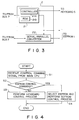
- the sub-CPU 2 has functions to operate as a keyboard controller for controlling the keyboard 5 and to perform erase/read/write of data stored in the EEPROM 1. Further, as shown in Fig. 3, the sub-CPU 2 has a determination processing circuit 21 and a serial/parallel converter 22.
- the determination processing circuit 21 includes a controller 21a and a ROM 21b, receives a control command signal output from the main CPU 3 via the bus 7, and performs a determination process of the received control command signal. More specifically, control commands having keyboard control commands and EEPROM control commands are stored in the ROM 21b previously, and the controller 21a determines whether a control command included in the control command signal is the EEPROM control command or the keyboard control command by comparing the control command included in the control command signal with the control command stored in the ROM 21b. When the control command is the keyboard control command, keyboard control is performed, and when the control command is the EEPROM control command, control of the EEPROM is executed. Responsive to the kind of the EEPROM control command, erase/read/write operations are performed.
- the serial/parallel converter 22 converts parallel data from the bus 7 into serial data and serial data from the EEPROM 1 into parallel data.
- the main CPU 3 controls the entire system and outputs control command signals, etc. to the sub-CPU 2.
- the memory 4 stores a system control program and application programs.
- the CMOS RAM 6 is utilized for a backup of the data, etc.
- the sub-CPU 2, main CPU 3, memory 4 and CMOS RAM 6 are interconnected to the bus 7.
- a control command signal from the main CPU 3 is received in step S1.
- step S2 it is determined that whether or not the control command included in the received control command signal is an EEPROM control command.
- the received control command is compared with the control command stored in the ROM 21b.
- step S2 when the received control command is not the EEPROM control command, it is determined that the received control command is a keyboard control command and keyboard control process is performed (step S3).
- step S2 when the received control command is the EEPROM control command, the EEPROM 1 is selected and EEPROM control process is performed (step S4). That is, erase/read/write of data are performed depending on the kind of the EEPROM control command.
- control of the EEPROM is performed by providing a control command signal from the main CPU to the sub-CPU capable of erasing/reading out/writing data with respect to the EEPROM, without modifying a hardware for the control of a conventional main CPU and further without providing an additional input/output port.
Landscapes
- Engineering & Computer Science (AREA)
- Theoretical Computer Science (AREA)
- General Engineering & Computer Science (AREA)
- Computer Hardware Design (AREA)
- Physics & Mathematics (AREA)
- General Physics & Mathematics (AREA)
- Software Systems (AREA)
- Read Only Memory (AREA)
- Programmable Controllers (AREA)
- Multi Processors (AREA)
Claims (4)
- Computersystem mit einer Zentraleinheit (CPU) (3) zum Steuern des Computersystems, einer Einrichtung (7) zur Kommunikation von durch die CPU (3) zu verarbeitenden Daten, einer Datenspeichereinrichtung (4, 6) und einem Hilfs-Controller (2), der mit der Kommunikationseinrichtung (7) verbunden ist, einer Eingabe/Ausgabevorrichtung (5), die mit der Kommunikationseinrichtung durch den Hilfs-Controller (2) verbunden ist, einem elektrisch programmierbaren Speicher (1), der mit der Kommunikationseinrichtung (7) über den Hilfs-Controller (2) verbunden ist,
wobei die mit der Kommunikationseinrichtung (7) verbundene CPU (3) angeordnet ist zum Ausgeben von Steuerbefehlen mit einem Speichersteuerbefehl zum Steuern des elektrisch programmierbaren Speichers (1) und einem Eingabe/Ausgabevorrichtungs- Steuerbefehl zum Steuern der Eingabe/Ausgabe-Vorrichtung (5),
wobei der Hilfs-Controller (2) aufweist:
eine Einrichtung (21, S1) zum Empfangen des von der CPU (3) ausgegebenen Steuerbefehls,
eine Einrichtung (21a, 21b, S2) zum Bestimmen, ob der empfangene Steuerbefehl der Speichersteuerbefehl oder Eingabe/Ausgabevorrichtungs-Steuerbefehl ist, und
eine Einrichtung (21, S3, S4) zum wahlweisen Durchführen eines Speicherzugriffsteuerprozesses zum Speichern von Daten in dem elektrisch programmierbaren Speicher (1),wenn der empfangene Steuerbefehl der Speichersteuerbefehl ist, und eines Eingabe/Ausgabe-Steuerprozesses zum Steuern der Eingabe/Ausgabe-Vorrichtung, wenn der empfange Steuerbefehl der Vorrichtungssteuerbefhel ist. - Computersystem nach Anspruch 1, dadurch gekennzeichnet, daß der Speichersteuerbefehl wenigstens einen Datenlöschbefehl, einen Datenlesebefehl und einen Datenschreibbefehl umfaßt.
- Computersystem nach Anspruch 1 oder 2, dadurch gekennzeichnet, daß die Eingabe/Ausgabe-Vorrichtung (5) ein Tastenfeld umfaßt.
- Computersystem nach einem der Ansprüche 1 bis 3, dadurch gekennzeichnet, daß der elektrisch programmierbare Speicher (1) einen elektrisch löschbaren programmierbaren Festwertspeicher umfaßt.
Applications Claiming Priority (2)
| Application Number | Priority Date | Filing Date | Title |
|---|---|---|---|
| JP258765/89 | 1989-10-05 | ||
| JP1258765A JPH03122752A (ja) | 1989-10-05 | 1989-10-05 | パーソナルコンピュータ |
Publications (3)
| Publication Number | Publication Date |
|---|---|
| EP0421425A2 EP0421425A2 (de) | 1991-04-10 |
| EP0421425A3 EP0421425A3 (en) | 1992-06-03 |
| EP0421425B1 true EP0421425B1 (de) | 1995-08-09 |
Family
ID=17324778
Family Applications (1)
| Application Number | Title | Priority Date | Filing Date |
|---|---|---|---|
| EP90119055A Expired - Lifetime EP0421425B1 (de) | 1989-10-05 | 1990-10-04 | Speicher-Steuersystem |
Country Status (4)
| Country | Link |
|---|---|
| EP (1) | EP0421425B1 (de) |
| JP (1) | JPH03122752A (de) |
| KR (1) | KR940002341B1 (de) |
| DE (1) | DE69021478T2 (de) |
Families Citing this family (1)
| Publication number | Priority date | Publication date | Assignee | Title |
|---|---|---|---|---|
| EP0416321B1 (de) * | 1989-08-28 | 1994-11-09 | Chisso Corporation | Kristalline Polyolefinmischung |
Family Cites Families (3)
| Publication number | Priority date | Publication date | Assignee | Title |
|---|---|---|---|---|
| JPS60108953A (ja) * | 1983-11-15 | 1985-06-14 | モトローラ・インコーポレーテツド | メモリデータバスの多重化方法 |
| US4623986A (en) * | 1984-02-23 | 1986-11-18 | Texas Instruments Incorporated | Memory access controller having cycle number register for storing the number of column address cycles in a multiple column address/single row address memory access cycle |
| GB8710917D0 (en) * | 1987-05-08 | 1987-06-10 | Cambridge Computer Ltd | Digital computers |
-
1989
- 1989-10-05 JP JP1258765A patent/JPH03122752A/ja active Pending
-
1990
- 1990-10-04 EP EP90119055A patent/EP0421425B1/de not_active Expired - Lifetime
- 1990-10-04 DE DE69021478T patent/DE69021478T2/de not_active Expired - Fee Related
- 1990-10-05 KR KR1019900015949A patent/KR940002341B1/ko not_active Expired - Fee Related
Non-Patent Citations (2)
| Title |
|---|
| A. LESEA, R. ZAKS: MICROPROCESSOR INTERFACE TECHNIKEN, MSB, MARKDORF, DE, 1979, pages 47-49 * |
| May 1988, HONOLULU, HAWAII pages 152 - 159; B.SPRUNT ET AL.: 'Priority-Driven,Preemptive I/O Controllers for Real-Time Systems' * |
Also Published As
| Publication number | Publication date |
|---|---|
| KR910008579A (ko) | 1991-05-31 |
| JPH03122752A (ja) | 1991-05-24 |
| DE69021478D1 (de) | 1995-09-14 |
| EP0421425A2 (de) | 1991-04-10 |
| EP0421425A3 (en) | 1992-06-03 |
| KR940002341B1 (ko) | 1994-03-23 |
| DE69021478T2 (de) | 1996-01-25 |
Similar Documents
| Publication | Publication Date | Title |
|---|---|---|
| US5623620A (en) | Special test modes for a page buffer shared resource in a memory device | |
| EP1531480B1 (de) | Speicherschaltung | |
| JP3947781B2 (ja) | 低電圧単一電源フラッシュメモリのためのプログラムアルゴリズム | |
| US5361343A (en) | Microprocessor system including first and second nonvolatile memory arrays which may be simultaneously read and reprogrammed | |
| US6834322B2 (en) | Nonvolatile semiconductor memory device having plural memory circuits selectively controlled by a master chip enable terminal or an input command and outputting a pass/fail result | |
| US4905140A (en) | Semiconductor integrated circuit device | |
| US5802552A (en) | System and method for allocating and sharingpage buffers for a flash memory device | |
| US4718038A (en) | Data security device for storing data at a peripheral part of the device during power down thus preventing improper retrieval | |
| EP0592069B1 (de) | Elektrisch löschbare nichtflüchtige Halbleiterspeicheranordnung für selektiven Gebrauch in "boot block" oder normalen Flashspeicheranordnungen | |
| KR100265266B1 (ko) | 플래쉬 eeprom 을 구비하는 마이크로컴퓨터및 플래쉬 eeprom 의 소거방법 | |
| US6442068B1 (en) | Non-volatile memory with functional capability of burst mode read and page mode read during suspension of an operation of electrical alteration | |
| EP0428396B1 (de) | Bitfehlerkorrekturschaltung für einen nichtflüchtigen Speicher | |
| US7305514B2 (en) | Command sequence for optimized power consumption | |
| EP0374733B1 (de) | Einchip-Mikrorechner mit EPROM | |
| EP0421425B1 (de) | Speicher-Steuersystem | |
| US6532529B1 (en) | Microcomputer including flash memory overwritable during operation and operating method thereof | |
| US20030021163A1 (en) | Semiconductor memory device and information device | |
| KR950008440B1 (ko) | 비트 클리어 및 레지스터 초기화 기능을 갖는 반도체 기억 회로 | |
| EP0508829B1 (de) | IC-Karte | |
| US5619714A (en) | Microcomputer having an instruction decoder with a fixed area and a rewritable area | |
| JPH10143434A (ja) | 半導体集積回路 | |
| KR20000005052A (ko) | 반도체 저장 장치 | |
| JPH11259357A (ja) | 半導体集積装置及び不揮発性メモリ書き込み方式 | |
| JPH0697442B2 (ja) | マイクロコンピユ−タ | |
| JP3135770B2 (ja) | 不揮発性半導体メモリおよびその不揮発性半導体メモリを使用した記憶装置 |
Legal Events
| Date | Code | Title | Description |
|---|---|---|---|
| PUAI | Public reference made under article 153(3) epc to a published international application that has entered the european phase |
Free format text: ORIGINAL CODE: 0009012 |
|
| 17P | Request for examination filed |
Effective date: 19901031 |
|
| AK | Designated contracting states |
Kind code of ref document: A2 Designated state(s): DE FR GB |
|
| PUAL | Search report despatched |
Free format text: ORIGINAL CODE: 0009013 |
|
| AK | Designated contracting states |
Kind code of ref document: A3 Designated state(s): DE FR GB |
|
| 17Q | First examination report despatched |
Effective date: 19940629 |
|
| GRAA | (expected) grant |
Free format text: ORIGINAL CODE: 0009210 |
|
| AK | Designated contracting states |
Kind code of ref document: B1 Designated state(s): DE FR GB |
|
| REF | Corresponds to: |
Ref document number: 69021478 Country of ref document: DE Date of ref document: 19950914 |
|
| ET | Fr: translation filed | ||
| PLBE | No opposition filed within time limit |
Free format text: ORIGINAL CODE: 0009261 |
|
| STAA | Information on the status of an ep patent application or granted ep patent |
Free format text: STATUS: NO OPPOSITION FILED WITHIN TIME LIMIT |
|
| 26N | No opposition filed | ||
| PGFP | Annual fee paid to national office [announced via postgrant information from national office to epo] |
Ref country code: GB Payment date: 19970925 Year of fee payment: 8 |
|
| PGFP | Annual fee paid to national office [announced via postgrant information from national office to epo] |
Ref country code: FR Payment date: 19971009 Year of fee payment: 8 |
|
| PGFP | Annual fee paid to national office [announced via postgrant information from national office to epo] |
Ref country code: DE Payment date: 19971010 Year of fee payment: 8 |
|
| PG25 | Lapsed in a contracting state [announced via postgrant information from national office to epo] |
Ref country code: GB Free format text: LAPSE BECAUSE OF NON-PAYMENT OF DUE FEES Effective date: 19981004 |
|
| GBPC | Gb: european patent ceased through non-payment of renewal fee |
Effective date: 19981004 |
|
| PG25 | Lapsed in a contracting state [announced via postgrant information from national office to epo] |
Ref country code: FR Free format text: LAPSE BECAUSE OF NON-PAYMENT OF DUE FEES Effective date: 19990630 |
|
| REG | Reference to a national code |
Ref country code: FR Ref legal event code: ST |
|
| PG25 | Lapsed in a contracting state [announced via postgrant information from national office to epo] |
Ref country code: DE Free format text: LAPSE BECAUSE OF NON-PAYMENT OF DUE FEES Effective date: 19990803 |