EP0422606A2 - Dispositif semi-conducteur comprenant des E2PROM et des EPROM dans une puce - Google Patents
Dispositif semi-conducteur comprenant des E2PROM et des EPROM dans une puce Download PDFInfo
- Publication number
- EP0422606A2 EP0422606A2 EP90119407A EP90119407A EP0422606A2 EP 0422606 A2 EP0422606 A2 EP 0422606A2 EP 90119407 A EP90119407 A EP 90119407A EP 90119407 A EP90119407 A EP 90119407A EP 0422606 A2 EP0422606 A2 EP 0422606A2
- Authority
- EP
- European Patent Office
- Prior art keywords
- sheet resistance
- gate
- ρsd
- ρsc
- substrate
- Prior art date
- Legal status (The legal status is an assumption and is not a legal conclusion. Google has not performed a legal analysis and makes no representation as to the accuracy of the status listed.)
- Granted
Links
Images




















Classifications
-
- H—ELECTRICITY
- H10—SEMICONDUCTOR DEVICES; ELECTRIC SOLID-STATE DEVICES NOT OTHERWISE PROVIDED FOR
- H10B—ELECTRONIC MEMORY DEVICES
- H10B41/00—Electrically erasable-and-programmable ROM [EEPROM] devices comprising floating gates
- H10B41/40—Electrically erasable-and-programmable ROM [EEPROM] devices comprising floating gates characterised by the peripheral circuit region
-
- H—ELECTRICITY
- H10—SEMICONDUCTOR DEVICES; ELECTRIC SOLID-STATE DEVICES NOT OTHERWISE PROVIDED FOR
- H10B—ELECTRONIC MEMORY DEVICES
- H10B41/00—Electrically erasable-and-programmable ROM [EEPROM] devices comprising floating gates
- H10B41/40—Electrically erasable-and-programmable ROM [EEPROM] devices comprising floating gates characterised by the peripheral circuit region
- H10B41/42—Simultaneous manufacture of periphery and memory cells
- H10B41/43—Simultaneous manufacture of periphery and memory cells comprising only one type of peripheral transistor
- H10B41/47—Simultaneous manufacture of periphery and memory cells comprising only one type of peripheral transistor with a floating-gate layer also being used as part of the peripheral transistor
Definitions
- the present invention relates to a semiconductor and, more particularly, to a semiconductor device having an E2PROM and an EPROM in one chip.
- a RAM and a ROM are formed on one chip.
- the RAM is constituted by an SRAM
- the ROM is constituted by an EPROM or the like.
- a semiconductor device characterized by comprising a semiconductor substrate of a first conductivity type having a major surface, first, second, third, and fourth semiconductor regions of a second conductivity type which are separately formed in a major surface region of the substrate, first carrier storage means, formed above the substrate between the first and second semiconductor regions, for storing carriers, first insulating means, formed between the first carrier storage means and the substrate, for electrically insulating the first carrier storage means from the substrate, a first conductive layer formed above the first carrier storage means and having a sheet resistance of ⁇ sA, second insulating means, formed between the first conductive layer and the first carrier storage means, for insulating the first conductive layer from the first carrier storage means, second carrier storage means, formed above the substrate between the third and fourth semiconductor regions and formed above the fourth region so as to partly overlap the fourth region, for storing carriers, third insulating means, formed between the second carrier storage means, the substrate, and the fourth semiconductor region, for electrically insulating the
- first and second carrier storage layers are arranged.
- a tunnel insulating film is formed on a third insulating layer between the second carrier storage layer and a fourth semiconductor region serving as a source/drain region.
- carriers can be electrically injected and extracted in and from the second carrier storage layer. That is, the second carrier storage layer serves as a floating gate of an E2PROM memory cell.
- the E2PROM capable of electrically writing and erasing data is used as a RAM.
- the area of one E2PROM memory cell is smaller than that of one SRAM memory cell. Therefore, if the RAM is constituted by E2PROM memory cells, the area occupied by the RAM in one chip can be decreased, and the storage capacity of the RAM can be increased.
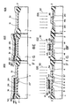
- Fig. 1 is a sectional view showing a semiconductor device according to the first embodiment of the present invention.
- field oxide films 2 are formed on a semiconductor substrate, e.g., a silicon substrate 1. With this arrangement, element isolation is performed.
- a first gate insulating film 5 is formed on the substrate 1 between one of the source/drain regions 3 and the source/drain region 3′.
- the first gate insulating film 5 consists of, e.g., a silicon oxide film, and has a thickness of, e.g., about 430 ⁇ .
- a tunnel insulating film 5′ is formed on the impurity layer 4.
- the tunnel insulating film 5′ consists of, e.g., a silicon oxide film having a thickness of about 100 ⁇ .
- a floating gate 6 consisting of a first polysilicon layer is formed on the first gate insulating film 5 and the tunnel insulating film 5′.
- a gate insulating film 7 is formed on the substrate 1 between the other source/drain region 3 and the source/drain region 3′.
- the gate insulating film 7 consists of, e.g., a silicon oxide film and has a thickness of, e.g., about 430 ⁇ . The thickness of the film 7 is almost the same as that of the first gate insulating film 5.
- a gate 8 consisting of the first polysilicon layer is formed on the gate insulating film 7.
- a transistor which has this gate 8 is a select transistor for selecting an E2PROM memory cell.
- a transistor having the gate 8 and the gate 8 will be respectively referred to as a "select transistor” and a “select gate” hereinafter.
- a transistor which has the floating gate 6 and a control gate 10 will be referred to as a "memory cell transistor” hereinafter.
- a second gate insulating film 9 consisting of, e.g., a silicon oxide film is formed on the floating gate 6.
- the control gate 10 consisting of a second polysilicon layer is formed on the second gate insulating film 9.
- An insulating interlayer 11 is formed on the entire upper surface of the device.
- Contact holes 12 are formed in the insulating interlayer 11 so as to communicate with the source/drain regions 3.
- Wires 12′ consisting of, e.g., aluminum are respectively formed in the contact holes 12.
- a surface protective film 13 is formed on the insulating interlayer 11.
- a first gate insulating film 15 is formed on the substrate 1 between the source/drain regions 14.
- a first gate insulating film 15 consists of, e.g., a silicon oxide film and has a thickness of about 250 ⁇ .
- a floating gate 16 consisting of a first polysilicon layer is formed on the first gate insulating film 15.
- a second gate insulating film 17 consisting of, e.g., a silicon oxide film is formed on the floating gate 16.
- a control gate 18 consisting of a second polysilicon layer is formed on the second gate insulting film 17.
- the insulating interlayer 11 is formed on the upper entire surface of the device.
- Contact holes 19 are formed in the insulating interlayer 11 so as to communicate with the source/drain regions 14.
- Wires 19′ consisting of, e.g., aluminum are respectively formed in the contact holes 19.
- the surface protective film 13 is formed on the insulating interlayer 11.
- each of the E2PROM and the EPROM shown in Fig. 1 is of a so-called "two-bus scheme" in which the wires are respectively connected to the source and drain.
- a gate insulating film 21 is formed on the substrate 1 between the source/drain regions 20.
- This gate insulating film 21 consists of, e.g., a silicon oxide film and has a thickness of, e.g., about 250 ⁇ .
- a gate 22 of a MOSFET constituting a peripheral circuit e.g., various types of decoders), a logic circuit, or the like is formed on the gate insulating film 21.
- the gate 22 consists of a first polysilicon layer.
- An insulating interlayer 11 is formed on the entire upper surface of the device.
- Contact holes 23 consisting of, e.g., aluminum are in the insulating interlayer 11 so as to communicate with the source/drain regions 20.
- Wires 23′ consisting of, e.g., aluminum are respectively formed in the contact holes 23.
- the surface protective film 13 is formed on the insulating interlayer 11.
- the tunnel insulating film 5′ having a thickness of about 100 ⁇ is formed between the floating gate 6 and the impurity layer 4 so as to constitute a nonvolatile memory cell called a "FLOTOX (floating-gate tunnel oxide)".
- FLOTOX floating-gate tunnel oxide
- Data is stored depending on whether the memory cell transistor is turned on in accordance with the charge state of the floating gate 6.
- Carriers are injected into the floating gate 6 by, e.g., applying a positive potential to the control gate 10 and grounding the source/drain region 3′. With this operation, the electrons from the source/drain region 3′ tunnel through the tunnel insulating film 5′ and are injected into the floating gate 6.
- Carriers are extracted from the floating gate 6 by, e.g., applying a positive potential to the source/drain region 3′ and grounding the control gate 10. With this operation, the electrons tunnel through the tunnel insulating film 5′ and are injected into the source/drain region 3′.
- the semiconductor device having the above-described arrangement includes a memory cell having the floating gate 16 formed between the control gate 18 and the substrate 1 and having no tunnel insulating film.
- a memory cell of this type is a nonvolatile memory cell called an "SAMOS (Stacked-gate Avalanche-injection MOS)".
- SAMOS Stacked-gate Avalanche-injection MOS
- the memory cell has no tunnel insulating film. For this reason, injection of carriers (electrons) into the floating gate 16 is performed by, e.g., generating hot electrons in the substrate 1 (channel) between the source and the drain, applying a positive potential to the control gate 18, and injecting the hot electrons into the floating gate 16.
- Extraction of carriers (electrons) from the floating gate 16 is performed by, e.g., exciting electrons in the floating gate 16 upon radiation of ultraviolet rays, and causing the electrons to escape to the source/drain regions 14 and the like over the barrier of the gate insulating film 15.
- the memory cell having the floating gate 16 therefore, can electrically write data and can erase data by an erase method other than an electrical method, e.g., a method using ultraviolet rays or the like.
- an E2PROM capable of electrically erasing data and an EPROM capable of erasing data by an erase method other than an electrical method are formed on the same substrate 1. That is, a semiconductor device having an E2PROM and an EPROM in one chip can be obtained.
- the above-described semiconductor device can be applied to, e.g., a one-chip microcomputer in which a RAM and a ROM are mounted together.
- an E2PROM Since an E2PROM is capable of electrically erasing data, it is used as a RAM, and an EPROM is used as a ROM. If a RAM is constituted by E2PROM memory cells each having the above-described arrangement, the area occupied by the RAM in one chip is decreased, and the packing density of the RAM, i.e., the storage capacity, can be increased. This is because the area of one E2PROM memory cell is about 1/5 that of, e.g, one SRAM memory cell. In addition, a CPU or the like for accessing the ROM and the RAM is constituted by a MOSFET.
- an E2PROM has the characteristics of both RAM and ROM. Therefore, even if the power source for the chip is turned off, data can be held. An SRAM cannot perform such a data holding operation after the power source is turned off.
- an E2PROM and an EPROM are formed on one chip, if a system or the like constituted by an E2PROM and an EPROM of different chips is constituted by the semiconductor device according to the present invention, these elements can be integrated into one chip. Therefore, a simple, high-performance system can be realized.
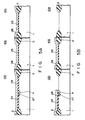
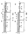
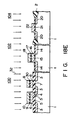
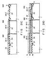
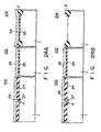
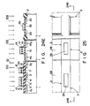
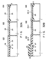
- FIGS. 2A to 2H are sectional views showing the steps in manufacturing the semiconductor device according to the first embodiment of the present invention.
- the same reference numerals in Figs. 2A to 2H denote the same parts as in Fig. 1.
- field oxide films 2 are selectively formed on the upper surface of a silicon substrate 1 of, e.g., a p type by using, e.g., a LOCOS method, thus performing element isolation.
- First thermal oxide films 24 are formed on the exposed surface portions of the substrate 1 by, e.g., thermal oxidation.
- An n-type impurity layer 4 is formed at a predetermined position of the substrate 1 in an E2PROM memory cell region 100 by, e.g., photoetching and selective ion implantation of As.
- reference numerals 102 and 104 respectively denote an EPROM memory cell and a MOSFET.
- the first thermal oxide films 24 formed in the regions 102 and 104 on the upper surface of the substrate 1 are removed to expose the upper surface of the substrate 1.
- second thermal oxide films 25 are formed on surface portions of the substrate 1 corresponding to the regions 102 and 104 by, e.g., thermal oxidation.
- the first thermal oxide film 24 is also grown to slightly increase its due to the heat generated during this thermal oxidation.
- a portion of the first thermal oxide film 24 on the impurity layer 4 is selectively removed by, e.g., photoetching.
- the portion from which the film 24 is removed is denoted by reference numeral 26.
- a third thermal oxide film 27 is then formed on a surface portion of the substrate 1 corresponding to the portion 26 by, e.g., thermal oxidation. Owing to the heat during the thermal oxidation, the first and second thermal oxide films 24 and 25 are also grown, and their thicknesses are slightly increased.
- a first polysilicon layer 28 is formed on the entire upper surface of the device by, e.g., CVD.
- the growth of the first to third thermal oxide films 24, 25, and 27 is stopped.
- the first, second, and third thermal oxide films 24, 25, and 27 respectively have thicknesses of, e.g., about 430 ⁇ , 250 ⁇ , and 100 ⁇ . These thicknesses are not limited to the above values but may be set to be optimal values, respectively.
- phosphorus is diffused in the first polysilicon layer 28 by, e.g., POCl3 to render it conductive so as to have a desired sheet resistance ⁇ s.
- ion implantation of an impurity or doping of an impurity into the first polysilicon layer 28 may be performed in advance.
- the first polysilicon layer 28 is selectively etched by, e.g., photoetching. As a result, a select gate pattern 28′ and a gate pattern 28′ of the MOSFET are formed.
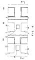
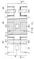
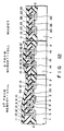
- Fig. 3 is a plan view showing the device in this step.
- Fig. 2F is a sectional view taken along a line 2F - 2F in Fig. 3.
- the first polysilicon layer 28 is patterned into the respective gate patterns 28′.
- cell slits 29 for isolating the floating gate in units of memory cells are simultaneously formed. These cell slits are formed in the field oxide films 2.
- a fourth thermal oxide film 30 is formed on the upper surfaces of the first polysilicon layers 28 and the respective gate patterns 28′ by, e.g., thermal oxidation.
- the fourth thermal oxide film 30 serves as second gate insulating films of the E2PROM memory cell and the EPROM memory cell.
- the thickness of the fourth thermal oxide film 30 is optimally set in accordance with the characteristics of the E2PROM memory cell and of the EPROM memory cell.
- a second polysilicon layer 31 is then formed on the entire upper surface of the device by, e.g., CVD. Phosphorus is diffused in the second polysilicon layer 31 to render it conductive so as to have a desired sheet resistance ⁇ s.
- ion implantation of an impurity or doping of an impurity into the second polysilicon layer 31 may be performed in advance.
- a photoresist (not shown) is coated on the entire upper surface of the device. Portions of the photoresist (not shown) located on the region 104 and near the select transistor in the region 100 are selectively removed by photoetching. Subsequently, the second polysilicon layer 31 is selectively removed by using the photoresist (not shown) as a mask. The photoresist (not shown) is then peeled off. Another photoresist (not shown) is coated on the entire upper surface of the device. The control gate patterns of the E2PROM and EPROM memory cells are formed by photoetching using the photoresist (not shown). At this time, the upper surfaces of the region 104 and the select transistor are covered with the photoresist. Thereafter, the second polysilicon layer 31, the fourth thermal oxide film 30, and the first polysilicon layer 28 are sequentially etched.
- the following gates and films are formed in the region 100: the first gate insulating film 5 consisting of the first thermal oxide film 24; the tunnel insulating film 5′ consisting of the third thermal oxide film 27; the floating gate 6 consisting of the first polysilicon layer 28; the second gate insulating film 9 consisting of the fourth thermal oxide film 30; and the control gate 10 consisting of the second polysilicon layer 31.
- the gate insulating film 7 consisting of the fourth thermal oxide film 30, and the select gate 8 consisting of the first polysilicon layer 28 are formed.
- the following gates and films are formed in the region 102: the gate insulating film 15 consisting of the second thermal oxide film; the floating gate 16 of the memory cell, which consists of the first polysilicon layer 28; the second gate insulating film 17 consisting of the fourth thermal oxide film; and the control gate 18 consisting of the second polysilicon layer 31.
- the gate insulating film 21 consisting of the second thermal oxide film 25, and the gate 22 consisting of the first polysilicon layer 28 are formed.
- the insulating interlayer 11 is then formed on the entire upper surface of the device by, e.g., CVD.
- the insulating interlayer 11 is selectively etched to form the contact holes 12, 19, and 23 communicating with predetermined portions of the device by, e.g., photoethcing.
- An aluminum film is formed on the entire upper surface of the resultant structure by, e.g., sputtering.
- the aluminum film is selectively etched by, e.g., photoetching to form the metal wires 12′, 19′, and 23′.
- the surface protective film 13 is formed on the entire upper surface of the device by, e.g., CVD.
- the semiconductor device according to the first embodiment is manufactured.
- an E2PROM and an EPROM can be formed on the same substrate together.
- the sheet resistances of the first and second polysilicon layers in the first embodiment are respectively represented by ⁇ sA and ⁇ sB
- the sheet resistances of the respective conductive members are given as follows: floating gate 6: ⁇ sA control gate 10: ⁇ sB select gate 8: ⁇ sA floating gate 16: ⁇ sA control gate 18: ⁇ sB gate 22: ⁇ sA
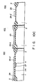
- Fig. 4 is a sectional view showing a semiconductor device according to the second embodiment of the present invention.
- the same reference numerals in Fig. 4 denote the same parts as in Fig. 1, and only different portions will be described below.
- the sheet resistances of the control gate 10, the select gate 34, and the control gates 6 and 18 can be set to be smaller than those of the floating gates 6 and 16. That is, if the resistances of the select gate 34, the gate 36, and the control gates 10 and 18 can be set to be smaller than those of the floating gates 6 and 16, the resistance of each gate wire can be reduced.
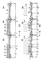
- FIGS. 5A to 5D are sectional views showing the steps in manufacturing the semiconductor device according to the second embodiment of the present invention.
- the same reference numerals in Figs. 5A to 5D denote the same parts as in Figs. 2A to 2H, and only different portions will be described below.
- FIG. 5A A structure shown in Fig. 5A is obtained through the above-described steps shown in Figs. 2A to 2E.
- the structure shown in Fig. 5A is identical to that shown in Fig. 2E.
- a first polysilicon layer 28 is selectively etched by, e.g., photoetching. As a result, portions of the first polysilicon layer 28 which are located near the select transistor of the E2PROM and on a region 104 are removed.
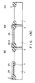
- Fig. 6 is a plan view showing the structure at this time.
- Fig. 5B is a sectional view taken along a line 5B - 5B in Fig. 6. As shown in Fig. 6, when the first polysilicon layer 28 is selectively etched, cell slits 29 are simultaneously formed.
- a fourth thermal oxide film 30 is formed on the upper surface of the first polysilicon layer 28 and an exposed surface portion of a first substrate 1.
- the fourth thermal oxide film 30 serves as the second gate insulating films of the E2PROM and EPROM memory cells and as the gate insulating films of a select transistor and a MOSFET.
- a second polysilicon layer 31 is formed on the entire upper surface of the device by, e.g., CVD. Phosphorus is then diffused in the second polysilicon layer 31 by, e.g., POCl3 to render it conductive so as to have a desired sheet resistance ⁇ s.
- a photoresist (not shown) is coated on the entire upper surface of the device.
- a select gate pattern and a gate pattern of the MOSFET are formed by photoetching using the photoresist (not shown).
- the upper surfaces of a region 102 and the E2PROM memory transistor are covered with this photoresist.
- the second polysilicon layer 31 is etched by using the photoresist (not shown) as a mask.
- the photoresist is the peeled off.
- a photoresist (not shown) is coated on the entire upper surface of the device again.
- Control gate patterns of the E2PROM and EPROM memory cells are formed by photoetching using the photoresist (not shown). At this time, the upper surfaces of a region 104 and the select transistor are covered with the photoresist.
- the second polysilicon layer 31, the fourth thermal oxide 30, and the first polysilicon layer 28 are sequentially etched by using the photoresist (not shown).
- a first gate insulating film 5 consisting of a first thermal oxide film 24
- a tunnel insulating film 5′ consisting of a second thermal oxide film 27
- the floating gate 6 consisting of the first polysilicon layer 28
- a second gate insulating film 9 consisting of the fourth thermal oxide film 30
- the control gate 10 consisting of the second polysilicon layer 31.
- a gate insulating film 33 consisting of the fourth oxide film 30, and the select gate 34 consisting of the second polysilicon layer 31 are formed.
- the following films and gates are formed in the region 102: a gate insulating film 15 consisting of the second thermal oxide film 30; the floating gate 16 consisting of the first polysilicon layer 28; a second gate insulating film 17 consisting of the fourth thermal oxide film; and the control gate 18 consisting of the second polysilicon layer 31.
- a gate insulating film 35 consisting of the fourth thermal oxide film 30, and the gate 36 consisting of the second polysilicon layer 28 are formed in the region 104.
- the semiconductor device according to the second embodiment of the present invention is manufactured.
- control gates 10 and 18, the select gate 34, and the gate 36 are set to have sheet resistances different from those of the floating gates 6 and 16, and hence the E2PROM and the EPROM can be formed on the same substrate.
- the sheet resistances of the first and second polysilicon layers are respectively represented by ⁇ sA and ⁇ sB
- the sheet resistances of the respective conductive members are given as follows: floating gate 6: ⁇ sA control gate 10: ⁇ sB select gate 8: ⁇ sB floating gate 16: ⁇ sA control gate 18: ⁇ sB gate 22: ⁇ sB
- Fig. 7 is a sectional view showing a semiconductor device according to the third embodiment of the present invention.
- the same reference numerals in Fig. 7 denote the same parts as in Fig. 1, and only different portions will be described below.
- the second gate insulating film of an E2PROM is constituted by a four-layered film consisting of an oxide film 38, a nitride film 39, an oxide film 40, and a nitride film 41
- the second gate insulating film of an EPROM is constituted by a four-layered film consisting of an oxide film 42, a nitride film 43, an oxide film 44, and a nitride film 45.
- the relationship between the sheet resistances of the respective conductive layers in the semiconductor device according to the third embodiment is the same as that in the second embodiment.
- the capacitance between a control gate and a floating gate can be increased.
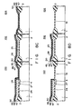
- FIG. 8A to 8F are sectional views showing the steps in manufacturing the semiconductor device according to the third embodiment of the present invention.
- the same reference numerals in Figs. 8A to 8F denote the same parts as in Figs. 2A to 2H, and only different portions will be described below.
- FIG. 8A A structure shown in Fig. 8A is obtained through the above-described steps in Figs. 2A to 2E.
- the structure shown in Fig. 8A is identical to that shown in Fig. 2E.
- a first polysilicon layer 28 is selectively etched by, e.g., photoetching. As a result, portions of the first polysilicon layer 28 which are located near the select transistor of an E2PROM and on a region 104 are removed.
- the surface obtained at this time is identical to, e.g., the surface shown in Fig. 6.
- a fifth thermal oxide film 47 is formed on the upper surface of the first polysilicon layer 28 and exposed surface portions of the substrate 1.
- conditions for thermal oxidation are set such that a thermal oxide film having a thickness of about 350 ⁇ is formed the upper surface of the first polysilicon layer 28 in an atmosphere of N2 with a dilution ratio of 20% at a temperature 1,000°C.
- a first nitride film 48 is formed on the entire upper surface of the device to have a thickness of about 300 ⁇ by, e.g., CVD.
- a sixth thermal oxide film 49 is formed on the upper surface of the first nitride film 48 by, e.g., thermal oxidation.
- conditions for the thermal oxidation are set such that a thermal oxide film having a thickness of about 60 ⁇ is formed on the upper surface of the first nitride film 48 in an atmosphere of BOx (boron oxide) at a temperature of 950°C for 80 minutes.
- a second nitride film 50 is then formed on the entire upper surface of the device to have a thickness of about 300 ⁇ by, e.g., CVD.
- the fifth thermal oxide film 47, the first nitride film 48, the sixth thermal oxide film 49, and the second nitride film 50 are selectively and sequentially etched by, e.g., photoetching.
- portions of the fifth thermal oxide film 47, of the first nitride film 48, of the sixth thermal oxide film 49, and of the second nitride film 50 which are located near the select transistor of the E2PROM and on a region 104 are removed.
- a seventh thermal oxide film 51 is then formed on exposed surface portions of the substrate 1.
- the seventh thermal oxide film 51 serves as the gate insulating films of the select transistor and a MOSFET.
- a second polysilicon layer 31 is formed on the entire upper surface of the device by, e.g., CVD. Phosphorus is then diffused in the second polysilicon layer 31 by, e.g., POCl3 to render it conductive so as to have a desired sheet resistance ⁇ s.
- a first gate insulating film 5 consisting of a first thermal oxide film 24
- a tunnel insulating film 5′ consisting of a third thermal oxide film 27
- the floating gate 6 consisting of the first polysilicon layer 28
- the second gate insulating film consisting of the four-layered film
- the control gate 10 consisting of the second polysilicon layer 31.
- a gate insulating film 33 consisting of a seventh thermal oxide film 51, and the select gate 34 consisting of the second polysilicon layer 31 are formed.
- a gate insulating film 15 consisting of a second thermal oxide film 30
- the floating gate 16 consisting of the first polysilicon layer 28
- the second gate insulating film consisting of the four-layered film
- a control gate 18 consisting of the second polysilicon layer 31.
- the semiconductor device according to the third embodiment is manufactured in the above-described steps.
- the second insulating film formed between the control gate and the floating gate is constituted by, e.g., a four-layered film consisting of oxide and nitride films, thereby allowing an E2PROM and an EPROM to be formed on the same substrate.
- the sheet resistances of the first and second polysilicon layers are respectively represented by ⁇ sA and ⁇ sB
- the sheet resistances of the respective conductive members are given as follows: floating gate 6: ⁇ sA control gate 10: ⁇ sB select gate 8: ⁇ sB floating gate 16: ⁇ sA control gate 18: ⁇ sB gate 22: ⁇ sB
- Fig. 9 is a sectional view showing a semiconductor device according to the fourth embodiment of the present invention.
- the same reference numerals in Fig. 9 denote the same parts as in Fig. 1, and only different portions will be described below.
- the sheet resistances of the following gates are: floating gate 6: ⁇ s1 floating gate 53: ⁇ s2 select gate 52: ⁇ s3 gate 54: ⁇ s4 control gate 10: ⁇ s5 control gate 18: ⁇ s6
- the respective sheet resistances have the following relationships: ⁇ s1 ⁇ ⁇ s2 (4)
- ⁇ s5 ⁇ s6 (6)
- the relationship of inequality (4) is defined by ⁇ s1 > ⁇ s2 (7) especially the reliability of the E2PROM memory cell can be improved.
- the inequality (7) is established when the impurity concentration of the floating gate 6 of the E2PROM memory cell is lower than that of the floating gate 53 of the EPROM memory cell. If the impurity concentration of the floating gate 6 is set to be low, leakage of carriers (electrons) from the floating gate 6 into an impurity layer 4 through a tunnel insulating film 5′ can be prevented. In addition, leakage of an impurity from the floating gate 6 into the impurity layer 4 through the tunnel insulating film 5′ can be prevented. Therefore, when the EPROM memory cell and the E2PROM memory cell are formed on the same substrate together, especially the reliability of the E2PROM memory cell can be improved.
- FIG. 10A to 10C are sectional views showing the steps in manufacturing the semiconductor device according to the fourth embodiment of the present invention.
- the same reference numerals in Figs. 10A to 10C denote the same parts as in Figs. 2A to 2H, and only different portions will be described below.
- FIG. 10A A structure shown in Fig. 10A is obtained through the above-described steps in Figs. 2A to 2E.
- the structure shown in Fig. 10A is identical to that shown in Fig. 2E.
- a thermal oxide film 55 is formed on the upper surface of a first polysilicon layer 28 by, e.g., thermal oxidation.
- the thermal oxide film has a thickness of, e.g., about 400 ⁇ .
- the thermal oxide film 55 is selectively removed by, e.g., photoetching. As a result, a portion of the thermal oxide film 55 is left on a surface portion of the polysilicon layer 28 serving as a floating gate in a region 100.
- Phosphorus is diffused in the first polysilicon layer 28 by, e.g., POCl3 to render it conductive.
- a portion 28-2 having a high impurity concentration and a portion 28 having a low impurity concentration are formed in the first polysilicon layer 28.
- the portion 28 having the low impurity concentration has an impurity concentration of about 1 to 3 ⁇ 1020 cm ⁇ 3
- the portion 28-2 having the high impurity concentration has an impurity concentration of about 4 to 6 ⁇ 1020 cm ⁇ 3.
- a method of rendering the polysilicon layer 28 conductive is not limited to the above. For example, ion implantation may be employed.
- a mask for preventing impurity diffusion may be constituted not only by a thermal oxide film 55 but also by a CVD oxide film or a photoresist having an impurity blocking effect.
- Fig. 10C the first polysilicon layer 28 is selectively etched by, e.g., photoetching. As a result, a select gate pattern and a gate pattern 28-2′ are formed.
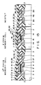
- Fig. 11 is a plan view of the resultant structure.
- Fig. 10C is a sectional view taken along a line 10C - 10C in Fig. 11. As shown in Fig. 11, when the first polysilicon layer 28 is selectively etched, cell slits 29 are simultaneously formed.
- the semiconductor device according to the fourth embodiment is manufactured.
- the sheet resistances ⁇ s1 and ⁇ s2 of the floating gates 6 and 53 of the E2PROM and EPROM memory cells are set to be different from each other, thereby allowing the E2PROM and the EPROM to be formed on the same substrate.
- the sheet resistances of the respective conductive members are given as follows: floating gate 6: ⁇ sA control gate 10: ⁇ sB select gate 52: ⁇ sA′ floating gate 53: ⁇ sA′ control gate 10: ⁇ sB gate 54: ⁇ sA′
- Fig. 12 is a sectional view showing a semiconductor device according to the fifth embodiment of the present invention.
- the same reference numerals in Fig. 12 denote the same parts as in Fig. 1, and only different portions will be described below.
- the respective sheet resistances of the respective gates are: floating gate 6: ⁇ s1 floating gate 53: ⁇ s2 select gate 34: ⁇ s3 gate 36: ⁇ s4 control gate 10: ⁇ s5 control gate 18: ⁇ s6
- the respective sheet resistances have the following relationships: ⁇ s1 ⁇ ⁇ s2 (8)
- the relationship of inequality (8) is defined by: ⁇ s1 ⁇ ⁇ s2 (9) then, similar to the fourth embodiment, the reliability of the E2PROM memory cell can be improved.
- each of the select gate 34, the gate 36, and the control gates 10 and 18 has a sheet resistance different from that of the floating gate 6, the resistance of each gate wire can be reduced as described with reference to, e.g., the second embodiment.
- FIG. 13A to 13C are sectional views showing the steps in manufacturing the semiconductor device according to the fifth embodiment of the present invention.
- the same reference numerals in Figs. 13A to 13C denote the same parts as in Figs. 2A to 2H, and only different portions will be described below.
- FIG. 13A A structure shown in Fig. 13A is obtained through the above-described steps in Figs. 2A to 2E.
- the structure shown in Fig. 13A is identical to that shown in Fig. 2E.
- a thermal oxide film 55 is formed on the upper surface of a first polysilicon layer 28 in the same step as, e.g., that shown in Fig. 10B.
- the thermal oxide film 55 is selectively removed by, e.g., photoethcing to leave a portion of the thermal oxide film 55 on a surface portion of the first polysilicon layer 28 serving as a floating gate in a region 100.
- Phosphorus is then diffused in the first polysilicon layer 28 by, e.g., POCl3 to render it conductive.
- a portion 28-2 having a high impurity concentration and a portion 28 having a low impurity concentration are formed in the first polysilicon layer 28 by using the thermal oxide film 55 as a mask for controlling impurity diffusion.
- the impurity concentration of the portion 28 having the high impurity concentration is set to be about 1 to 3 ⁇ 1020 cm ⁇ 3
- the impurity concentration of the portion 28 having the low impurity concentration is set to be about 4 to 6 ⁇ 1020 cm ⁇ 3.
- the first polysilicon layer 28 is selectively etched by, e.g., photoetching to remove portions of the first polysilicon layer 28 which are located near the select transistor of the E2PROM and on a region 104.
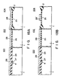
- Fig. 14 is a plan view showing the resultant structure.
- Fig. 13C is a sectional view taken along a line 13C - 13C in Fig. 14. As shown in Fig. 13, when the first polysilicon layer 28 is selectively etched, cell slits 29 are simultaneously formed.
- the semiconductor device according to the fifth embodiment is manufactured.
- the sheet resistance of the floating gate 6 of the E2PROM memory cell is set to be different from that of the floating gate 53 of the EPROM memory cell so that the E2PROM and the EPROM can be formed on the same substrate.
- the select gate 34 and the gate 36 are constituted by a second polysilicon layer, the sheet resistance of each of the select gate 34 and the gate 36 can be set to be different from that of the floating gate 6 or the floating gate 53.
- the sheet resistance of the first polysilicon layer is represented by ⁇ sA; the sheet resistance of the first polysilicon layer in which an impurity is doped, by ⁇ sA′; and the sheet resistance of the second polysilicon layer, by ⁇ sB, the sheet resistances of the respective conductive members are: floating gate 6: ⁇ sA control gate 10: ⁇ sB select gate 34: ⁇ sB floating gate 53: ⁇ sA′ control gate 18: ⁇ sB gate 36: ⁇ sB
- Fig. 15 is a sectional view showing a semiconductor device according to the sixth embodiment of the present invention.
- the same reference numerals in Fig. 15 denote the same parts as in Fig. 1, and only different portions will be described below.
- the second gate insulating film of the E2PROM memory cell is constituted by a four-layered film consisting of an oxide film 38, a nitride film 39, an oxide film 40, and a nitride film 41
- the second gate insulating film of the EPROM memory cell is also constituted by a four-layered film consisting of an oxide film 42, a nitride film 43, an oxide film 44, and a nitride film 45.
- the sheet resistances of the respective conductive layers have the same relationships as those of the sheet resistances in the fifth embodiment.
- the capacitances between a control gate 10 and a floating gate 6 and between a control gate 18 and a floating gate 53 can be increased.
- the reliability of the E2PROM memory cell can be improved, and the resistance of each gate wire can be further reduced.
- FIGS. 16A to 16D are sectional views showing the steps in manufacturing the semiconductor device according to the sixth embodiment of the present invention.
- the same reference numerals in Figs. 16A to 16D denote the same parts as in Figs. 2A to 2H, and only different portions will be described below.
- FIG. 16A A structure shown in Fig. 16A is obtained through the above-described steps in Figs. 2A to 2E.
- the structure shown in Fig. 16A is identical to that shown in Fig. 2E.
- a structure shown in Fig. 16B is obtained in the step shown in Fig. 13B.
- a structure shown in Fig. 16C is obtained in the step shown in Fig. 13C.
- a structure shown in Fig. 16D is obtained in the step shown in Fig. 8C.
- the semiconductor device according to the sixth embodiment is manufactured.
- the E2PROM and the EPROM can be formed on the same substrate. Since a select gate 34 and a gate 36 are composed of a second polysilicon layer, the sheet resistances of the select gate 34 and the gate 36 can be set to be different from those of the floating gates 6 and 53. In addition to these advantages, a second gate insulating film between a control gate and a floating gate can be composed of a stacked layer consisting of an oxide film and a nitride film.
- the sheet resistance of the first polysilicon layer is represented by ⁇ sA; the sheet resistance of the first polysilicon layer in which an impurity is doped, by ⁇ sA′; and the sheet resistance of the second polysilicon layer, by ⁇ sB, the sheet resistances of the respective conductive members are: floating gate 6: ⁇ sA control gate 10: ⁇ sB select gate 52: ⁇ sB floating gate 16: ⁇ sA′ control gate 18: ⁇ sB gate 36: ⁇ sB
- Fig. 17 is a sectional view showing a semiconductor device according to the seventh embodiment of the present invention.
- the same reference numerals in Fig. 17 denote the same parts as in Figs 1, and only different portions will be described below.
- a second polysilicon layer 8′ is left above a select gate 8.
- a select gate of this type is generally called a "stacked select gate”.
- a memory cell transistor is constituted by two layers of a floating gate 6 and a control gate 10.
- a select transistor is constituted by two layers of the select gate 8 and the second polysilicon layer 8′.
- FIGS. 18A to 18E are sectional views showing the steps in manufacturing the semiconductor device according to the seventh embodiment of the present invention.
- the same reference numerals in Figs. 18A to 18E denote the same parts as in Figs. 2A to 2H, and only different portions will be described below.
- FIG. 18A A structure shown in Fig. 18A is obtained through the above-described steps in Figs. 2A to 2E.
- the structure shown in Fig. 18A is identical to that shown in Fig. 2E.
- a first polysilicon layer 28 is selectively etched by, e.g., photoethcing.
- a gate pattern 28′ of the MOSFET constituting a peripheral circuit is formed in a region 104.
- Fig. 19 is a plan view showing the resultant structure.
- Fig. 18B is a sectional view taken along a line 18B - 18B in Fig. 19.
- cell slits 29 are simultaneously formed.
- a fourth thermal oxide film 30 is formed on the upper surfaces of the first polysilicon layer 28 and the gate pattern 28′ by, e.g., thermal oxidation.
- a second polysilicon layer 31 is then formed on the entire surface of the device by, e.g., CVD. Phosphorus is diffused in the second polysilicon layer 31 by, e.g., POCl3 to render it conductive.
- the second polysilicon layer 31 is selectively etched by, e.g., photoethcing. With this process, a portion of the second polysilicon layer 31 on the region 104 is removed. At the same time, the second polysilicon layer 31 at an end portion of a select gate (not shown) is selectively removed to form an exposed portion of a first polysilicon layer 28. The portion serves as a region in which a wire is to contact with the gate 8.
- the second polysilicon layer 31, a fourth thermal oxide film 30, and the first polysilicon layer 28 are selectively etched by, e.g., photoetching.
- the following films and gates are formed in a region 100: a first insulating film 5 consisting of a first thermal oxide film 24; a tunnel insulating film 5′ consisting of a third thermal oxide film 27; the floating gate 6 consisting of the first polysilicon layer 28; a second gate insulating film 9 consisting of the fourth thermal oxide film 30; a control gate 10 consisting of the second polysilicon layer 31; a gate insulating film 7 consisting of a first thermal oxide film 24; and the select gate 8 consisting of the first polysilicon layer 28.
- the second polysilicon layer 8′ is formed above the select gate 8.
- the following films and gates are formed in a region 102: a first gate insulating film 15 consisting of a second thermal oxide film 25; a floating gate 16 consisting of the first polysilicon layer 28; a second gate insulating film 17 consisting of the fourth thermal oxide film 30; and a control gate 18 consisting of the second polysilicon layer 31.
- a gate insulating film 21 consisting of the second thermal oxide film 25 and a gate 22 consisting of the first polysilicon layer 28 are formed in the region 104.
- the semiconductor device according to the seventh embodiment is manufactured.
- the gate patterns of the select and memory cell transistors can be patterns in the same step.
- Fig. 20 is a sectional view showing a semiconductor device according to the eighth embodiment of the present invention.
- the same reference numerals in Fig. 20 denote the same parts as in Fig. 1, and only different portions will be described below.
- a second polysilicon layer 52′ is left above a select gate 52 to form a stacked select gate.
- the sheet resistances of the respective gates are: floating gate 6: ⁇ s1 floating gate 53: ⁇ s2 select gate 52: ⁇ s3 gate 54: ⁇ s4 control gate 10: ⁇ s5 control gate 18: ⁇ s6
- the respective sheet resistances have the following relationships: ⁇ s1 ⁇ ⁇ s2 (11)
- ⁇ s5 ⁇ s6 (13)
- FIG. 21A to 21D are sectional views showing the steps in manufacturing the semiconductor device according to the eighth embodiment of the present invention.
- the same reference numerals in Fig. 21A to 21D denote the same parts as in Figs. 2A to 2H, and only different portions will be described below.
- FIG. 21A A structure shown in Fig. 21A is obtained through the above-described steps in Figs. 2A to 2E.
- the structure shown in Fig. 2A is identical to that shown in Fig. 2E.
- a thermal oxide film 55 is formed on the upper surface of a first polysilicon layer 28 by, e.g., thermal oxidation.
- the thermal oxide film 55 is then selectively removed by, e.g., photoetching.
- a portion of the thermal oxide film 55 is left on a surface portion of the first polysilicon layer 28 which serves as a floating gate.
- Phosphorus is diffused in the first polysilicon layer 28 by, e.g., POCl3 to render it conductive.
- almost no phosphorus is diffused in a portion of the first polysilicon layer 28 under the thermal oxide film 55 because the film 55 serves as a mask for controlling impurity diffusion.
- a portion 28-2 having a high impurity concentration and a portion 28 having a low impurity concentration are formed in the first polysilicon layer 28.
- the first polysilicon layer 28 is selectively etched by, e.g., photoetching. As a result, a gate pattern 28-2′ of the MOSFET is formed.
- Fig. 22 shows the resultant structure.
- Fig. 21C is a sectional view taken along a line 21C - 21C in Fig. 22.
- cell slits 29 are simultaneously formed.
- a thermal oxide film 30 is formed on the upper surfaces of the first polysilicon layers 28 and 28-2′ by, e.g., thermal oxidation.
- a second polysilicon layer 31 is then formed on the entire upper surface of the device by, e.g., CVD.
- the semiconductor device according to the eighth embodiment is manufactured.
- the gate portions of the select and memory cell transistors can be patterned in the same step.
- the sheet resistances of the floating gates 6 and 53 can be set to be different from each other.
- the sheet resistance of the first polysilicon layer is represented by ⁇ sA; the sheet resistance of the first polysilicon layer in which an impurity is doped, by ⁇ sA′; and the sheet resistance of the second polysilicon layer, by ⁇ sB, the sheet resistances of the respective conductive members are: floating gate 6: ⁇ sA control gate 10: ⁇ sB select gate 52: ⁇ sA′ floating gate 53: ⁇ sA′ control gate 18: ⁇ sB gate 54: psA′
- Fig. 23 is a sectional view showing a semiconductor device according to the ninth embodiment of the present invention.
- the same reference numerals in Fig. 23 denote the same parts as in Fig. 1, and only different portions will be described below.
- a second polysilicon layer 8′ is left above a select gate 8 to form a stacked select gate.
- the sheet resistances of the respective gates are: floating gate 6: ⁇ s1 floating gate 16: ⁇ s2 select gate 8: ⁇ s3 gate 36: ⁇ s4 control gate 10: ⁇ s5 control gate 18: ⁇ s6
- the semiconductor device having the above-described arrangement since a stacked select gate is used, micropatterning of the E2PROM memory cell is facilitated, and the sheet resistance of, e.g., each of the floating gates 6 and 16 can be set to be smaller than that of the gate 36.
- FIGS. 24A to 24E are sectional views showing the steps in manufacturing the semiconductor device according to the ninth embodiment of the present invention.
- the same reference numerals in Figs. 24A to 24E denote the same parts as in Figs. 2A to 2H, and only different portions will be described below.
- FIG. 24A A structure shown in Fig. 24A is obtained through the above-described steps in Figs. 2A to 2E.
- the structure shown in Fig. 24A is identical to that shown in Fig. 2E.
- a first polysilicon layer 28 is selectively etched by, e.g., photoetching. As a result, a portion of the first polysilicon layer 28 on a region 104 is removed.
- Fig. 25 shows the resultant structure.
- Fig. 24B is a sectional view taken along a line 24B - 24B in Fig. 25. As shown in Fig. 25, when the first polysilicon layer 28 is selectively etched, cell slits 28 are simultaneously formed.
- a fourth thermal oxide film 30 is formed on the upper surface of the first polysilicon layer 28 and an exposed surface portion of the substrate 1.
- the fourth thermal oxide film 30 serves as the second gate insulating films of the E2PROM and EPROM memory cells and the gate insulating film of the MOSFET.
- a second polysilicon layer 31 is then formed on the entire upper surface of the device by, e.g., CVD. Phosphorus is diffused in the polysilicon layer 31 by, e.g., POCl3 to render it conductive so as to have a desired sheet resistance ⁇ s.
- the second polysilicon layer 31 is selectively etched by, e.g., photoetching. With this process, a gate pattern 31 of the MOSFET is formed in the region 104.
- the second polysilicon layer 31, the fourth thermal oxide film 30, and the first polysilicon layer 28 are selectively etched.
- the following films and gates are formed in a region 100: a first gate insulating film 5 consisting of a first thermal oxide film 24; a tunnel insulating film 5′ consisting of a third thermal oxide film 27; a floating gate 6 consisting of the first polysilicon layer 28; a second gate insulating film 9 consisting of the fourth thermal oxide film 30; the control gate 10 consisting of the second polysilicon layer 31; a gate insulating film 7 consisting of the first thermal oxide film 24; and the select gate 8 consisting of the first polysilicon layer 28.
- the second polysilicon layer 8′ is formed above the select gate 8.
- the following films and gates are formed in a region 102: a first gate insulating film 15 consisting of a second thermal oxide film 25; the floating gate 16 consisting of the first polysilicon layer 28; a second gate insulating film 17 consisting of the fourth thermal oxide film 30; and the control gate 18 consisting of the second polysilicon layer 31.
- a gate insulating film 35 consisting of the fourth thermal oxide film 30, and the gate 36 consisting of the second polysilicon layer 31 are formed in the region 104.
- the semiconductor device according to the ninth embodiment is manufactured.
- the gate portions of the select and memory cell transistors can be patterned in the same steps, and the sheet resistance of, e.g., each of the floating gates 6 and 16 can be set to be different from that of the gate 36.
- the sheet resistances of the first and second polysilicon layers are respectively represented by ⁇ sA and ⁇ sB
- the sheet resistances of the respective conductive layers are: floating gate 6: ⁇ sA control gate 10: ⁇ sB select gate 8: ⁇ sA floating gate 16: ⁇ sA control gate 18: ⁇ sB gate 36: ⁇ sB
- Fig. 26 is a sectional view showing a semiconductor device according to the tenth embodiment of the present invention.
- the same reference numerals in Fig. 26 denote the same parts as in Fig. 1, and only different portions will be described below.
- a second polysilicon layer 52′ is left above a select gate 52 to form a stacked select gate.
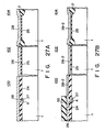
- FIGS. 27A to 27D are sectional views showing the steps in manufacturing the semiconductor device according to the tenth embodiment of the present invention.
- the same reference numerals in Figs. 27A to 27D denote the same parts as in Figs. 2A to 2H, and only different portions will be described below.
- FIG. 27A A structure shown in Fig. 27A is obtained through the above-described steps in Figs. 2A to 2E.
- the structure shown in Fig. 27A is identical to that shown in Fig. 2E.
- FIG. 27B A structure shown in Fig. 27B is obtained through the step in Fig. 21B.
- FIG. 27C A structure shown in Fig. 27C is obtained through the step in Fig. 24B.
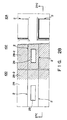
- Fig. 28 is a plan view showing the resultant structure.
- Fig. 27C is a sectional view taken along a line 27C - 27C in Fig. 28.
- FIG. 27D A structure shown in Fig. 27D is obtained through the step in Fig. 24C.
- the semiconductor device according to the tenth embodiment is manufactured.
- the gate portions of the select and memory cell transistors can be patterned in the same step, and the sheet resistances of the floating gates 6 and 53 can be set to be different from each other.
- the sheet resistances of the floating gate 6 and the gate 36 can be set to be different from each other.
- the sheet resistance of the first polysilicon layer is represented by ⁇ sA; the sheet resistance of the first polysilicon layer in which an impurity is doped, by ⁇ sA′; and the sheet resistance of the second polysilicon layer, by ⁇ sB, the sheet resistances of the respective conductive members are: floating gate 6: ⁇ sA control gate 10: ⁇ sB select gate 52: ⁇ sA′ floating gate 53: ⁇ sA′ control gate 18: ⁇ sB gate 36: ⁇ sB
- Fig. 29 is a sectional view showing a semiconductor device according to the eleventh embodiment of the present invention.
- the reference numerals in Fig. 29 denote the same parts as in Fig. 1, and only different portions will be described below.
- a second polysilicon layer 8′ is left above a select gate 8 to form a stacked select gate.
- the second gate insulating film of the E2PROM memory cell is constituted by a three-layered film consisting of an oxide film 38, a nitride film 39, and an oxide film 40
- the second gate insulating film of the EPROM memory cell is constituted by a three-layered film consisting of an oxide film 42, a nitride film 43, and an oxide film 44.
- the sheet resistances of the respective conductive layers have the same relationships as those in the ninth embodiment.
- the select gate is constituted by the stacked select gate, micropatterning of the E2PROM memory cell is facilitated, and the capacitance between a control gate and a floating gate can be increased.
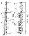
- FIG. 30A to 30F are sectional views showing the steps in manufacturing the semiconductor device according to the eleventh embodiment of the present invention.
- the same reference numerals in Figs. 30A to 30F denote the same parts as in Fig. 2A to 2H, and only different portions will be described below.
- FIG. 30A A structure shown in Fig. 30A is obtained through the above-described steps in Figs. 2A to 2E.
- the structure shown in Fig. 30A is identical to that shown in Fig. 2E.
- a structure shown in Fig. 30B is obtained through the step in Fig. 24B.
- a fifth thermal oxide film 47 is formed on the upper surface of a first polysilicon layer 28 and an exposed surface portion of the substrate 1 by, e.g., thermal oxidation.
- a first nitride film 48 is formed on the entire upper surface of the device.
- a sixth thermal oxide film 49 is formed on the upper surface of the first nitride film 48 by, e.g., thermal oxidation.
- the fifth thermal oxide film 47, the first nitride film 48, and the sixth thermal oxide film 49 are selectively and sequentially etched by, e.g., photoetching. As a result, portions of the fifth thermal oxide film 47, of the first nitride film 48, and of the sixth thermal oxide film 49 located in a region 104 are removed. Thereafter, a seventh thermal oxide film 51 is formed on the exposed surface portion of the substrate 1 by, e.g., thermal oxidation.
- the seventh thermal oxide film 51 serves as the gate insulating film of the MOSFET.
- a second polysilicon layer 31 is formed on the entire upper surface of the device by, e.g., CVD.
- a structure shown in Fig. 30F is obtained through the above-described steps in Figs. 24D to 24E.
- the following films and gates are formed in a region 100: a first gate insulating film 5 consisting of a first thermal oxide film 24; a tunnel insulating film 5′ consisting of a third thermal oxide film 27; a floating gate 6 consisting of a first polysilicon layer 28; the second gate insulating film consisting of the three-layered film; a control gate 10 consisting of a second polysilicon layer 31; a gate insulating film 7 consisting of the first thermal oxide film 24; and the select gate 8 consisting of the first polysilicon layer 28.
- the second polysilicon layer 8′ is formed above the select gate 8.
- the following films and gates are formed in a region 102: a first gate insulating film 15 consisting of a second thermal oxide film 25; a floating gate 16 consisting of the first polysilicon layer 28; the second gate insulating film consisting of the three-layered film; and a control gate 18 consisting of the second polysilicon layer 31.
- a gate insulating film 46 consisting of the seventh thermal oxide film 51, and a gate 36 consisting of the second polysilicon layer 31 are formed in the region 104.
- the semiconductor device according to the eleventh embodiment is manufactured.
- the gate portions of the select and memory cell transistors can be patterned in the same step.
- the E2PROM and the EPROM can be formed on the same substrate by using, e.g., a three-layered film consisting of oxide and nitride films as a second insulating film between a control gate and a floating gate.
- the sheet resistances of the first and second polysilicon layers are respectively represented by ⁇ sA and ⁇ sB
- the sheet resistances of the respective conductive layers are: floating gate 6: ⁇ sA control gate 10: ⁇ sB select gate 8: ⁇ sA floating gate 16: ⁇ sA control gate 18: ⁇ sB gate 36: ⁇ sB
- Fig. 31 is a sectional view showing a semiconductor device according to the twelfth embodiment of the present invention.
- the same reference numerals in Fig. 31 denote the same parts as in Fig. 1, and only different portions will be described below.
- a second polysilicon layer 52′ is left above a select gate 52 to form a stacked select gate.
- the second gate insulating film of the E2PROM memory cell is constituted by a three-layered film consisting of an oxide film 38, a nitride film 39, and an oxide film 40
- the second gate insulating film of the EPROM memory cell is constituted by a three-layered film consisting of an oxide film 42, a nitride film 43, and an oxide film 44.
- the sheet resistances of the respective conductive layers have the same relationships as those in the tenth embodiment.
- the capacitance between a control gate and a floating gate can be increased.
- the reliability of the E2PROM memory cell can be improved as in the fourth embodiment.
- FIGS. 32A to 32D are sectional views showing the steps in manufacturing the semiconductor device according to the twelfth embodiment of the present invention.
- the same reference numerals in Figs. 32A to 32D denote the same parts as in Figs. 2A to 2H, and only different portions will be described below.
- FIG. 32A A structure shown in Fig. 32A is obtained through the above-described steps in Figs. 2A to 2E.
- the structure shown in Fig. 32A is identical to that shown in Fig. 2E.
- a structure shown in Fig. 32B is obtained through the step in Fig. 27B.
- FIG. 32C A structure shown in Fig. 32C is obtained through the step in Fig. 30B.
- a structure shown in Fig. 32D is obtained through the step in Fig. 30C.
- the semiconductor device according to the twelfth embodiment is manufactured.
- the gate portions of the select and memory cell transistors can be patterned in the same step.
- the E2PROM and EPROM can be formed on the same substrate by using, e.g., a three-layered film consisting of oxide and nitride films as a second gate insulating film between a control gate and a floating gate.
- the sheet resistances of a floating gate 6 and of a gate 36 can be set to be different from each other.
- the sheet resistance of the first polysilicon layer is represented by ⁇ sA; the sheet resistance of the first polysilicon layer in which an impurity is doped, by ⁇ sA′; and the sheet resistance of the second polysilicon layer, by ⁇ sB, the sheet resistances of the respective conductive members are: floating gate 6: ⁇ sA control gate 10: ⁇ sB select gate 52: ⁇ sA floating gate 53: ⁇ sA control gate 18: ⁇ sB gate 36: ⁇ sB
Landscapes
- Engineering & Computer Science (AREA)
- Manufacturing & Machinery (AREA)
- Non-Volatile Memory (AREA)
- Semiconductor Memories (AREA)
Applications Claiming Priority (2)
| Application Number | Priority Date | Filing Date | Title |
|---|---|---|---|
| JP264453/89 | 1989-10-11 | ||
| JP1264453A JPH088314B2 (ja) | 1989-10-11 | 1989-10-11 | 不揮発性半導体記憶装置およびその製造方法 |
Publications (3)
| Publication Number | Publication Date |
|---|---|
| EP0422606A2 true EP0422606A2 (fr) | 1991-04-17 |
| EP0422606A3 EP0422606A3 (en) | 1992-01-22 |
| EP0422606B1 EP0422606B1 (fr) | 1996-06-05 |
Family
ID=17403414
Family Applications (1)
| Application Number | Title | Priority Date | Filing Date |
|---|---|---|---|
| EP90119407A Expired - Lifetime EP0422606B1 (fr) | 1989-10-11 | 1990-10-10 | Dispositif semi-conducteur comprenant des E2PROM et des EPROM dans une puce |
Country Status (5)
| Country | Link |
|---|---|
| US (1) | US5200636A (fr) |
| EP (1) | EP0422606B1 (fr) |
| JP (1) | JPH088314B2 (fr) |
| KR (1) | KR940006588B1 (fr) |
| DE (1) | DE69027271T2 (fr) |
Cited By (3)
| Publication number | Priority date | Publication date | Assignee | Title |
|---|---|---|---|---|
| EP0802569A1 (fr) * | 1996-04-15 | 1997-10-22 | STMicroelectronics S.r.l. | FLASH-EPROM intégrée avec une EEPROM |
| EP0994512A1 (fr) * | 1998-10-15 | 2000-04-19 | STMicroelectronics S.r.l. | Procédé de fabrication de cellules mémoire EEPROM non auto-alignées |
| WO2002052573A1 (fr) * | 2000-12-22 | 2002-07-04 | Koninklijke Philips Electronics N.V. | Dispositif semi-conducteur comportant une eeprom et une flash-eprom |
Families Citing this family (16)
| Publication number | Priority date | Publication date | Assignee | Title |
|---|---|---|---|---|
| US5355007A (en) * | 1990-11-23 | 1994-10-11 | Texas Instruments Incorporated | Devices for non-volatile memory, systems and methods |
| KR940009644B1 (ko) * | 1991-11-19 | 1994-10-15 | 삼성전자 주식회사 | 불휘발성 반도체메모리장치 및 그 제조방법 |
| JP3273582B2 (ja) * | 1994-05-13 | 2002-04-08 | キヤノン株式会社 | 記憶装置 |
| US5498560A (en) * | 1994-09-16 | 1996-03-12 | Motorola, Inc. | Process for forming an electrically programmable read-only memory cell |
| KR100350819B1 (ko) * | 1994-10-28 | 2003-01-15 | 코닌클리케 필립스 일렉트로닉스 엔.브이. | 전계효과장치 |
| US6787844B2 (en) * | 1995-09-29 | 2004-09-07 | Nippon Steel Corporation | Semiconductor device including transistor with composite gate structure and transistor with single gate structure, and method for manufacturing the same |
| JP3314807B2 (ja) | 1998-11-26 | 2002-08-19 | 日本電気株式会社 | 半導体装置の製造方法 |
| US6903434B2 (en) * | 1999-05-20 | 2005-06-07 | Alliance Semiconductors | Method and apparatus for integrating flash EPROM and SRAM cells on a common substrate |
| KR100375232B1 (ko) * | 2001-03-20 | 2003-03-08 | 삼성전자주식회사 | 비휘발성 메모리 소자의 제조방법 |
| JP2003282823A (ja) * | 2002-03-26 | 2003-10-03 | Toshiba Corp | 半導体集積回路 |
| US8050085B2 (en) | 2002-08-29 | 2011-11-01 | Renesas Electronics Corporation | Semiconductor processing device and IC card |
| JP2004200553A (ja) | 2002-12-20 | 2004-07-15 | Fujitsu Ltd | 半導体装置及びその製造方法 |
| US7256449B2 (en) * | 2003-05-20 | 2007-08-14 | Samsung Electronics, Co., Ltd. | EEPROM device for increasing a coupling ratio and fabrication method thereof |
| US20040232476A1 (en) * | 2003-05-20 | 2004-11-25 | Kang Sung-Taeg | EEPROM cell structures having non-uniform channel-dielectric thickness and methods of making the same |
| KR100604850B1 (ko) * | 2003-05-20 | 2006-07-31 | 삼성전자주식회사 | 균일하지 않은 채널 유전막 두께를 갖는 이이피롬 셀 구조및 그 제조방법 |
| US6998304B2 (en) * | 2004-03-01 | 2006-02-14 | Taiwan Semiconductor Manufacturing Co., Ltd. | Method for integrated manufacturing of split gate flash memory with high voltage MOSFETS |
Family Cites Families (11)
| Publication number | Priority date | Publication date | Assignee | Title |
|---|---|---|---|---|
| US4393474A (en) * | 1979-10-26 | 1983-07-12 | Texas Instruments Incorporated | EPROM and RAM cell layout with equal pitch for use in fault tolerant memory device or the like |
| JPS58166596A (ja) * | 1982-03-26 | 1983-10-01 | Mitsubishi Electric Corp | 半導体不揮発性記憶装置 |
| JPS596581A (ja) * | 1982-07-02 | 1984-01-13 | Mitsubishi Electric Corp | 半導体不揮発性記憶装置 |
| US4613956A (en) * | 1983-02-23 | 1986-09-23 | Texas Instruments Incorporated | Floating gate memory with improved dielectric |
| JPS60189971A (ja) * | 1984-03-09 | 1985-09-27 | Toshiba Corp | 半導体装置の製造方法 |
| US4698787A (en) * | 1984-11-21 | 1987-10-06 | Exel Microelectronics, Inc. | Single transistor electrically programmable memory device and method |
| FR2623651B1 (fr) * | 1987-11-20 | 1992-11-27 | Sgs Thomson Microelectronics | Plan memoire et procede et prototype de definition d'un circuit integre electronique comportant un tel plan memoire |
| US4833096A (en) * | 1988-01-19 | 1989-05-23 | Atmel Corporation | EEPROM fabrication process |
| DE3816358A1 (de) * | 1988-05-13 | 1989-11-23 | Eurosil Electronic Gmbh | Nichtfluechtige speicherzelle und verfahren zur herstellung |
| JP2790461B2 (ja) * | 1988-05-20 | 1998-08-27 | 株式会社日立製作所 | 半導体集積回路装置 |
| JPH02297970A (ja) * | 1989-05-12 | 1990-12-10 | Hitachi Ltd | 半導体集積回路装置 |
-
1989
- 1989-10-11 JP JP1264453A patent/JPH088314B2/ja not_active Expired - Fee Related
-
1990
- 1990-10-10 EP EP90119407A patent/EP0422606B1/fr not_active Expired - Lifetime
- 1990-10-10 US US07/594,173 patent/US5200636A/en not_active Expired - Lifetime
- 1990-10-10 DE DE69027271T patent/DE69027271T2/de not_active Expired - Fee Related
- 1990-10-11 KR KR1019900016087A patent/KR940006588B1/ko not_active Expired - Fee Related
Cited By (6)
| Publication number | Priority date | Publication date | Assignee | Title |
|---|---|---|---|---|
| EP0802569A1 (fr) * | 1996-04-15 | 1997-10-22 | STMicroelectronics S.r.l. | FLASH-EPROM intégrée avec une EEPROM |
| US5850092A (en) * | 1996-04-15 | 1998-12-15 | Sgs Thomson Microelectronics S.R.L. | FLASH-EPROM with embedded EEPROM |
| US6074916A (en) * | 1996-04-15 | 2000-06-13 | Sgs-Thomson Microelectronics S.R.L. | FLASH-EPROM with embedded EEPROM |
| EP0994512A1 (fr) * | 1998-10-15 | 2000-04-19 | STMicroelectronics S.r.l. | Procédé de fabrication de cellules mémoire EEPROM non auto-alignées |
| US6479347B1 (en) | 1998-10-15 | 2002-11-12 | Stmicroelectronics S.R.L. | Simplified DSCP process for manufacturing FLOTOX EEPROM non-autoaligned semiconductor memory cells |
| WO2002052573A1 (fr) * | 2000-12-22 | 2002-07-04 | Koninklijke Philips Electronics N.V. | Dispositif semi-conducteur comportant une eeprom et une flash-eprom |
Also Published As
| Publication number | Publication date |
|---|---|
| KR910008847A (ko) | 1991-05-31 |
| JPH088314B2 (ja) | 1996-01-29 |
| JPH03126265A (ja) | 1991-05-29 |
| KR940006588B1 (ko) | 1994-07-22 |
| EP0422606B1 (fr) | 1996-06-05 |
| DE69027271T2 (de) | 1996-12-19 |
| DE69027271D1 (de) | 1996-07-11 |
| US5200636A (en) | 1993-04-06 |
| EP0422606A3 (en) | 1992-01-22 |
Similar Documents
| Publication | Publication Date | Title |
|---|---|---|
| US6750525B2 (en) | Non-volatile memory device having a metal-oxide-nitride-oxide-semiconductor gate structure | |
| EP0422606A2 (fr) | Dispositif semi-conducteur comprenant des E2PROM et des EPROM dans une puce | |
| US5751039A (en) | Programmable non-volatile memory cell and method of forming a non-volatile memory cell | |
| US7563664B2 (en) | Semiconductor memory device equipped with memory transistor and peripheral transistor and method of manufacturing the same | |
| US5972751A (en) | Methods and arrangements for introducing nitrogen into a tunnel oxide in a non-volatile semiconductor memory device | |
| US6365457B1 (en) | Method for manufacturing nonvolatile memory device using self-aligned source process | |
| US5960283A (en) | Nonvolatile semiconductor memory device and method of fabrication of the same | |
| US20030203557A1 (en) | Method and structure for an improved floating gate memory cell | |
| US5532181A (en) | Method of manufacturing semiconductor non-volatile memory device having different gate insulating thicknesses | |
| EP0682364B1 (fr) | Procédé de fabrication d'un dispositif de mémoire rémanante à semi-conducteur | |
| JPH06112501A (ja) | 不揮発性半導体メモリ装置及びその製造方法 | |
| JP3241330B2 (ja) | フラッシュメモリおよびその製造方法 | |
| US7595237B2 (en) | Non-volatile memory cell with a hybrid access transistor | |
| KR20030014658A (ko) | 다양한 기술 및 애플리케이션에 대해 쉽게 수정가능한주변 트랜지스터를 갖는 셀프-얼라인 콘택 비휘발성메모리에 대한 구조 및 프로세스 | |
| US6608347B2 (en) | Semiconductor device and method of manufacturing the same | |
| JP3549364B2 (ja) | 三重ウェルを有するフラッシュ・メモリ・セルの製造方法 | |
| US6465303B1 (en) | Method of manufacturing spacer etch mask for silicon-oxide-nitride-oxide-silicon (SONOS) type nonvolatile memory | |
| US6756634B2 (en) | Gated semiconductor assemblies | |
| US7414282B2 (en) | Method of manufacturing a non-volatile memory device | |
| EP0383011A2 (fr) | Dispositif semi-conducteur de mémoire rémanente | |
| US20020106852A1 (en) | Lowered channel doping with source side boron implant for deep sub 0.18 micron flash memory cell | |
| JP2003060092A (ja) | 半導体記憶装置及びその製造方法 | |
| JPH09232454A (ja) | 不揮発性半導体装置及びその製造方法 | |
| JPH09232453A (ja) | 半導体装置及びその製造方法 | |
| KR20000014277A (ko) | 비휘발성 메모리소자 및 그 제조방법 |
Legal Events
| Date | Code | Title | Description |
|---|---|---|---|
| PUAI | Public reference made under article 153(3) epc to a published international application that has entered the european phase |
Free format text: ORIGINAL CODE: 0009012 |
|
| 17P | Request for examination filed |
Effective date: 19901010 |
|
| AK | Designated contracting states |
Kind code of ref document: A2 Designated state(s): DE FR GB |
|
| PUAL | Search report despatched |
Free format text: ORIGINAL CODE: 0009013 |
|
| AK | Designated contracting states |
Kind code of ref document: A3 Designated state(s): DE FR GB |
|
| 17Q | First examination report despatched |
Effective date: 19931105 |
|
| GRAH | Despatch of communication of intention to grant a patent |
Free format text: ORIGINAL CODE: EPIDOS IGRA |
|
| GRAA | (expected) grant |
Free format text: ORIGINAL CODE: 0009210 |
|
| AK | Designated contracting states |
Kind code of ref document: B1 Designated state(s): DE FR GB |
|
| REF | Corresponds to: |
Ref document number: 69027271 Country of ref document: DE Date of ref document: 19960711 |
|
| GRAH | Despatch of communication of intention to grant a patent |
Free format text: ORIGINAL CODE: EPIDOS IGRA |
|
| ET | Fr: translation filed | ||
| RIN2 | Information on inventor provided after grant (corrected) |
Free format text: UEMURA, TERUO, INTELLECTUAL * MIZUTANI, TAKAHIDE, INTELLECTUAL * HANADA, NAOKI, INTELLECTUAL * MORI, TATSUO, INTELLECTUAL * SHINADA, KAZUYOSHI, INTELLECTUAL/PROP. DIV., |
|
| PLBE | No opposition filed within time limit |
Free format text: ORIGINAL CODE: 0009261 |
|
| STAA | Information on the status of an ep patent application or granted ep patent |
Free format text: STATUS: NO OPPOSITION FILED WITHIN TIME LIMIT |
|
| 26N | No opposition filed | ||
| REG | Reference to a national code |
Ref country code: GB Ref legal event code: 746 Effective date: 19980910 |
|
| REG | Reference to a national code |
Ref country code: FR Ref legal event code: D6 |
|
| REG | Reference to a national code |
Ref country code: GB Ref legal event code: IF02 |
|
| PGFP | Annual fee paid to national office [announced via postgrant information from national office to epo] |
Ref country code: FR Payment date: 20021008 Year of fee payment: 13 |
|
| PGFP | Annual fee paid to national office [announced via postgrant information from national office to epo] |
Ref country code: GB Payment date: 20021009 Year of fee payment: 13 |
|
| PGFP | Annual fee paid to national office [announced via postgrant information from national office to epo] |
Ref country code: DE Payment date: 20021011 Year of fee payment: 13 |
|
| PG25 | Lapsed in a contracting state [announced via postgrant information from national office to epo] |
Ref country code: GB Free format text: LAPSE BECAUSE OF NON-PAYMENT OF DUE FEES Effective date: 20031010 |
|
| PG25 | Lapsed in a contracting state [announced via postgrant information from national office to epo] |
Ref country code: DE Free format text: LAPSE BECAUSE OF NON-PAYMENT OF DUE FEES Effective date: 20040501 |
|
| GBPC | Gb: european patent ceased through non-payment of renewal fee |
Effective date: 20031010 |
|
| PG25 | Lapsed in a contracting state [announced via postgrant information from national office to epo] |
Ref country code: FR Free format text: LAPSE BECAUSE OF NON-PAYMENT OF DUE FEES Effective date: 20040630 |
|
| REG | Reference to a national code |
Ref country code: FR Ref legal event code: ST |