EP0426035A2 - Optischer Kopf - Google Patents
Optischer Kopf Download PDFInfo
- Publication number
- EP0426035A2 EP0426035A2 EP90120598A EP90120598A EP0426035A2 EP 0426035 A2 EP0426035 A2 EP 0426035A2 EP 90120598 A EP90120598 A EP 90120598A EP 90120598 A EP90120598 A EP 90120598A EP 0426035 A2 EP0426035 A2 EP 0426035A2
- Authority
- EP
- European Patent Office
- Prior art keywords
- detection output
- optical head
- optical
- photodiode
- semiconductor laser
- Prior art date
- Legal status (The legal status is an assumption and is not a legal conclusion. Google has not performed a legal analysis and makes no representation as to the accuracy of the status listed.)
- Granted
Links
- 230000003287 optical effect Effects 0.000 title claims abstract description 99
- 238000001514 detection method Methods 0.000 claims abstract description 56
- 239000004065 semiconductor Substances 0.000 claims abstract description 31
- 238000006243 chemical reaction Methods 0.000 claims description 7
- 239000003990 capacitor Substances 0.000 claims description 5
- 238000002834 transmittance Methods 0.000 description 8
- 238000004519 manufacturing process Methods 0.000 description 7
- 238000000034 method Methods 0.000 description 4
- 238000012423 maintenance Methods 0.000 description 3
- 230000005540 biological transmission Effects 0.000 description 2
- 238000010586 diagram Methods 0.000 description 1
- 230000002708 enhancing effect Effects 0.000 description 1
- 229920006395 saturated elastomer Polymers 0.000 description 1
Images

Classifications
-
- G—PHYSICS
- G11—INFORMATION STORAGE
- G11B—INFORMATION STORAGE BASED ON RELATIVE MOVEMENT BETWEEN RECORD CARRIER AND TRANSDUCER
- G11B7/00—Recording or reproducing by optical means, e.g. recording using a thermal beam of optical radiation by modifying optical properties or the physical structure, reproducing using an optical beam at lower power by sensing optical properties; Record carriers therefor
- G11B7/12—Heads, e.g. forming of the optical beam spot or modulation of the optical beam
- G11B7/13—Optical detectors therefor
Definitions
- the present invention relates to an optical head for use in optical information recording/reproducing devices. More particularly, it relates to an optical head capable of adjusting the detection output of an optical power detector employed for detecting the optical power of a semiconductor laser.
- a laser beam emitted by a semiconductor laser 22 is converted into a parallel beam of light by a collimating lens 23 and is split into a transmitted beam and a reflected beam by a beam splitter 24.
- the transmitted beam is converged upon a recording medium 26 by means of an objective lens 25 and is employed for recording or reading information.
- the feflected beam it impinges upon a photodiode 29 that is installed between and connected to output terminals 27 and 28, and here is converted into an electric signal. This electric signal is used as detection output for detecting the optical power of the semiconductor laser 22 to be sent by the optical head 21 to an external circuit.
- the optical power thereof varies greatly due to changes in temperature, elapse of time, or according to the current applied thereto.
- an APC Auto Power Control circuit, not shown, is usually accommodated outside of the optical head 21 and, using the detection output of the photodiode 29, the optical power of the semiconductor laser 22 is adjusted by means of the APC circuit so that a laser beam having a suitable light intensity is converged upon the recording medium 26.
- the detection output that the photodiode 29 releases is different in every optical head 21 manufactured making it difficult to accurately adjust the optical power of the semiconductor laser 22 by means of the APC circuit.
- the reason why the detection output released by the photodiode 29 varies will be discussed hereinbelow.
- the optical head 21 used for recording requires a strong light to perform the recording of information. Consequently, in order to obtain a laser beam having a high power of approximately 5mW to 15mW, provision is usually made such that the transmittance of the beam splitter 24 is high and the laser beam emitted by the semiconductor laser 22 is efficiently illuminated upon the recording medium 26. This is due to the fact that, under present mass production conditions, the maximum output of the semiconductor laser 22 is at most approximately equal to 40mW. It is therefore not possible to obtain a laser beam of a high power unless the beam splitter 24 has a high transmittance.
- the light intensity of the portion of the laser beam that was transmitted through the beam splitter 24 is represented by I t
- the light intensity I t stands in proportional relationship to the light intensity of the laser beam irradiated on the recording medium 26.
- the intensity of the light coming out from the objective lens 25 needs to be 5 to 10 times that of reproduction. Therefore, it is a prerequisite that no saturation occurs in any of the circuits following the photodiode 29 in order to correctly control the intensity of the light going out from the objective lens 25 during recording.
- the photodiode 29 has a wide dynamic range and usually does not get saturated, but circuits connected to the photodiode 29 such as the APC circuit, etc. are not able to release outputs above the power source voltage. This point needs to be taken in consideration when designing the circuitry, i.e. the gain of the APC circuit needs to be set such that the emission of a laser beam having a high power during recording does not cause the saturation of the circuit.
- the detection output released by the photodiode 29 varies greatly, the gains of circuits such as the APC circuit, etc. need to be set such that no saturation occurs, for the optical head 21 where the detection output released by the photodiode 29 is maximal.
- efficient use cannot be made of the dynamic range of the above circuits in the optical head 21 where the detection output released by the photodiode 29 is minimal. Namely, if in the optical head 21 the detection output is minimal, the detection output released by the photodiode 29 during reproduction is of a low level and has a low S/N whereby the optical power of the semiconductor laser 22 cannot be adjusted as desired.
- the detection output released by the photodiode 29 is converted from an analog signal into a digital signal and the optical power of the semiconductor laser 22 is digitally controlled, the accuracy in setting the optical power of the semiconductor laser 22 drops significantly in the optical head 21 where the detection output of the photodiode 29 is small, due to a low resolution per bit.
- An object of the present invention is to provide an optical head capable of adjusting the detection output released by an optical power detector employed for detecting the intensity of the light illuminated on a recording medium.
- Another object of the present invention is to provide an optical head permitting to omit the process of adjusting the gain of an APC circuit during the manufacturing process of the optical head.
- an optical head comprises a semiconductor laser that emits a laser beam, an optical system for leading the light emitted by the semiconductor laser to a recording medium, an optical power detector for detecting the power of the light emitted by the semiconductor laser, and detection output adjusting means for adjusting a detection output released by the optical power detector.
- the detection output adjusting means may be designed such as to mainly adjust electrically the detection output released by the optical power detector, or may also be designed such as to adjust the intensity of the laser beam impinging upon the optical power detector.
- the implementation of the detection output adjusting means permits to adjust the detection output released by the optical power detector employed for detecting the intensity of the light emitted by the optical head.
- Such an arrangement thus enables to prevent the detection output released by the optical power detector from fluctuating thereby permitting to eliminate the need for adjusting the gain of the APC circuit during the manufacturing process of the optical head.
- the cost increase caused by adjusting the gain of the APC circuit may be restrained and the maintenance, such as the replacement of the optical head, etc. may be facilitated.
- the wide dynamic range of the APC circuit may efficiently be made use of, and the power of the light emitted by the semiconductor laser may be controlled in a highly acciirate manner according to a detection output having a satisfying signal-to-noise ratio.
- the above arrangement may also be adopted for eliminating through the action of the detection output adjusting means, the fluctuation of the detection output released by the optical power detector caused by factors other than the accuracy of the optical system.
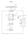
- an optical head 1 of the present embodiment comprises a semiconductor laser 2, an optical system 3, a photodiode 4 serving as optical power detector, and a variable resistor 5 serving as detection output adjusting means.
- the optical system 3 is composed of a collimating lens 6 that converts the laser beam emitted by the semiconductor laser 2 into a parallel beam of light, a beam splitter 7 that, after the laser beam passed through the collimating lens 6, transmits the laser beam with a predetermined transmittance and reflects it with a predetermined reflectance, and an objective lens 8 that converges upon a recording medium 9 the part of the laser beam that was transmitted through the beam splitter 7.
- the photodiode 4 is arranged such that the cathode thereof is connected to an output terminal 10 and the anode thereof is connected to an output terminal 11, and is grounded via the variable resistor 5.
- the photodiode 4 is placed at a position where it is capable of receiving the part of the laser beam that was reflected by the beam splitter 7.
- the variable resistor 5 is designed such that its resistance value R v can be adjusted within a given range so as to cancel the fluctuation of the detection output released by the photodiode 4 occurring with every optical head 1 when the optical head 1 is mass-produced.
- the laser beam emitted by the semiconductor laser 2 is converted into a parallel beam of light by the collimating lens 6.
- the part of the laser beam that passed through the beam splitter 7 is then converged onto the recording medium 9 by the objective lens 8, while the part of the laser beam that was reflected by the beam splitter 7 impinges upon the photodiode 4 that then produces a photocurrent I L .
- the value of the resistor R v should be set such as to be suitable for the circuit that is connected to and follows the variable resistor 5, and that is accommodated in the main body of the device carrying the optical head 1.
- the gain of the above circuit should preliminary be adjusted for the detection output V L so that no saturation occurs therein during recording.
- Such an arrangement enables to obtain a definite detection output V L irrespectively of the differences between each optical head 1, as the detection output V L can be adjusted by means of the variable resistor 5.
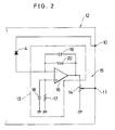
- the semiconductor laser 2 and the optical system 3 are not shown in Fig. 2 and their description will be omitted as they are disposed in the same manner as in the previous embodiment illustrated in Fig. 1.
- the members having the same function than in the aforementioned embodiment will be designated by the same code and their description will be omitted.
- an optical head 12 of the present embodiment comprises a detection output adjusting means 15 composed of a current-to-voltage conversion circuit 13 and a variable resistor 14.
- the optical head 12 is designed such that the cathode of the photodiode 4 is connected to the output terminal 10, and the anode of the same is connected to the inverting input terminal of an operational amplifier 16 housed in the current-to-voltage conversion circuit 13.
- the non-inverting input terminal of the operational amplifier 16 is grounded via a resistor 17 and a capacitor 18, the capacitor 18 being mounted in parallel with the resistor 17.
- a capacitor 19 and a resistor 20 are mounted in parallel and disposed between the inverting input terminal and the output terminal of the operational amplifier 16.
- the output terminal of the operational amplifier 16 is grounded via the variable resistor 14 whose adjustable terminal is connected to the output terminal 11 of the optical head 12.
- this arrangement enables the detection output of the photodiode 4 to be adjusted by means of the variable resistor 14.
- the present embodiment differs from the previous one in that the current-to-voltage conversion circuit 13 is disposed between the photodiode 4 and the variable resistor 14 and in that the photocurrent produced by the photodiode 4 that flew into the inverting input terminal of the operational amplifier 16 is converted into a voltage.
- the optical head 12 of the present embodiment thus presents the advantage that the frequency bandwidth may be set as desired iii the current-to-voltage conversion circuit 13.
- the detection output released by the photodiode 4 is adjusted electrically.
- the present invention is not limited to these examples and the detection output released by the photodiode 4 may also be adjusted optically.
- a filter or other member may for example be inserted in the section of the photodiode 4 whereon the laser light impinges.
- the previous and present embodiments adopted methods of detecting the optical power released by the semiconductor laser 2 by means of the laser light split by the beam splitter 7, but other methods may as well be employed.
- the optical power of the semiconductor laser 2 may, for example, be detected by installing a pin photodiode within a package housing the semiconductor laser 2 and employing it as photodetector.
- an optical head in accordance with the present invention comprises detection output adjusting means for adjusting the detection output released by an optical power detector.
- the fluctuation of the detection output released by the optical power detector occurring with every optical head due to the accuracy of the optical system or to other reason, may be thus eliminated by adjusting the detection output of the optical power detector through the detection output adjusting means.
- the detection output released by the optical power detector can be adjusted readily through the detection output adjusting means and there is no necessity of executing a laborious gain adjustment.
- efficient use can be made of the wide dynamic range of the APC circuit and the optical power of the semiconductor laser may be controlled in a highly accurate manner according to a detection output having a satisfying signal-to-noise ratio.
Landscapes
- Physics & Mathematics (AREA)
- Optics & Photonics (AREA)
- Optical Head (AREA)
Applications Claiming Priority (2)
| Application Number | Priority Date | Filing Date | Title |
|---|---|---|---|
| JP288323/89 | 1989-11-02 | ||
| JP1288323A JP2934264B2 (ja) | 1989-11-02 | 1989-11-02 | 光ピックアップ |
Publications (3)
| Publication Number | Publication Date |
|---|---|
| EP0426035A2 true EP0426035A2 (de) | 1991-05-08 |
| EP0426035A3 EP0426035A3 (en) | 1991-10-09 |
| EP0426035B1 EP0426035B1 (de) | 1995-12-20 |
Family
ID=17728695
Family Applications (1)
| Application Number | Title | Priority Date | Filing Date |
|---|---|---|---|
| EP90120598A Expired - Lifetime EP0426035B1 (de) | 1989-11-02 | 1990-10-26 | Optischer Kopf |
Country Status (4)
| Country | Link |
|---|---|
| US (1) | US5515350A (de) |
| EP (1) | EP0426035B1 (de) |
| JP (1) | JP2934264B2 (de) |
| DE (1) | DE69024329T2 (de) |
Cited By (3)
| Publication number | Priority date | Publication date | Assignee | Title |
|---|---|---|---|---|
| EP0881633A3 (de) * | 1997-05-29 | 1998-12-09 | Mitsumi Electric Company Ltd. | Laserstrahlemittierende Vorrichtung und mit dieser Vorrichtung versehener optischer Abtastkopf |
| GB2378334A (en) * | 2001-03-26 | 2003-02-05 | Agilent Technologies Inc | Fibre optic receiver with adjustable bandwidth post-amplifier |
| WO2003050808A1 (en) * | 2001-12-10 | 2003-06-19 | Thomson Licensing S.A. | Reproduction or recording apparatus for different optical recording media |
Families Citing this family (3)
| Publication number | Priority date | Publication date | Assignee | Title |
|---|---|---|---|---|
| JP3382846B2 (ja) * | 1998-05-11 | 2003-03-04 | 日本電気株式会社 | 光ヘッド及び光ヘッドに於ける光源出力のモニター方法 |
| KR100594239B1 (ko) * | 2004-01-28 | 2006-06-30 | 삼성전자주식회사 | 디지털 전위차계를 이용한 포토 다이오드의 감도 조정장치 및 방법 |
| JP2008176882A (ja) * | 2007-01-19 | 2008-07-31 | Sharp Corp | フロントモニタ装置ならびにそれを備える光ピックアップ装置および情報記録再生装置 |
Family Cites Families (14)
| Publication number | Priority date | Publication date | Assignee | Title |
|---|---|---|---|---|
| US4584687A (en) * | 1983-12-12 | 1986-04-22 | Optical Storage International-U.S. | Calibrated feedback for laser diodes |
| JPS60187074A (ja) * | 1984-03-07 | 1985-09-24 | Toshiba Corp | レ−ザダイオ−ドの自動光量調整回路 |
| US4675749A (en) * | 1984-03-16 | 1987-06-23 | Pioneer Electronic Corporation | Disc player system with digital information demodulation operation |
| JPS60247836A (ja) * | 1984-05-22 | 1985-12-07 | Nippon Gakki Seizo Kk | 光学式情報再生装置 |
| JPH0680554B2 (ja) * | 1985-02-08 | 1994-10-12 | オリンパス光学工業株式会社 | 2値化信号発生回路 |
| FR2584223B1 (fr) * | 1985-06-28 | 1994-06-17 | Thomson Alcatel Gigadisc | Memoire optique a suivi de piste echantillonne pour support d'information pregrave. |
| US4685097A (en) * | 1985-07-25 | 1987-08-04 | Laser Magnetic Storage International Company | Power control system for a semiconductor laser |
| JP2615553B2 (ja) * | 1985-11-14 | 1997-05-28 | 富士通株式会社 | レーザ制御装置 |
| JPS62150732U (de) * | 1986-03-17 | 1987-09-24 | ||
| JPH01112533A (ja) * | 1987-10-23 | 1989-05-01 | Mitsubishi Electric Corp | 光ディスク装置 |
| JPH01144243A (ja) * | 1987-11-30 | 1989-06-06 | Toshiba Corp | 情報記録装置 |
| JP2771821B2 (ja) * | 1988-08-31 | 1998-07-02 | オリンパス光学工業株式会社 | 発光体の光量制御装置 |
| GB2229268A (en) * | 1989-02-27 | 1990-09-19 | Philips Nv | Radiation emitting arrangement monitoring and controlling system |
| JPH02246027A (ja) * | 1989-03-17 | 1990-10-01 | Matsushita Electric Ind Co Ltd | 半導体レーザ駆動回路 |
-
1989
- 1989-11-02 JP JP1288323A patent/JP2934264B2/ja not_active Expired - Fee Related
-
1990
- 1990-10-26 DE DE69024329T patent/DE69024329T2/de not_active Expired - Lifetime
- 1990-10-26 EP EP90120598A patent/EP0426035B1/de not_active Expired - Lifetime
-
1993
- 1993-01-07 US US08/001,922 patent/US5515350A/en not_active Expired - Lifetime
Cited By (7)
| Publication number | Priority date | Publication date | Assignee | Title |
|---|---|---|---|---|
| EP0881633A3 (de) * | 1997-05-29 | 1998-12-09 | Mitsumi Electric Company Ltd. | Laserstrahlemittierende Vorrichtung und mit dieser Vorrichtung versehener optischer Abtastkopf |
| US6134210A (en) * | 1997-05-29 | 2000-10-17 | Mitsumi Electric Co., Ltd. | Laser beam emitting device and an optical pickup provided with the laser beam emitting device |
| GB2378334A (en) * | 2001-03-26 | 2003-02-05 | Agilent Technologies Inc | Fibre optic receiver with adjustable bandwidth post-amplifier |
| GB2378334B (en) * | 2001-03-26 | 2004-11-03 | Agilent Technologies Inc | Fiber optic receiver |
| US7072590B2 (en) | 2001-03-26 | 2006-07-04 | Avago Technologies General Ip Pte. Ltd. | Fiber optic receiver with an adjustable bandwidth post-amplifier |
| WO2003050808A1 (en) * | 2001-12-10 | 2003-06-19 | Thomson Licensing S.A. | Reproduction or recording apparatus for different optical recording media |
| US7130254B2 (en) | 2001-12-10 | 2006-10-31 | Thomson Licensing | Reproduction or recording apparatus for different optical recording media |
Also Published As
| Publication number | Publication date |
|---|---|
| EP0426035B1 (de) | 1995-12-20 |
| JP2934264B2 (ja) | 1999-08-16 |
| DE69024329T2 (de) | 1996-08-22 |
| JPH03147534A (ja) | 1991-06-24 |
| EP0426035A3 (en) | 1991-10-09 |
| US5515350A (en) | 1996-05-07 |
| DE69024329D1 (de) | 1996-02-01 |
Similar Documents
| Publication | Publication Date | Title |
|---|---|---|
| US6858830B2 (en) | Optical receiver apparatus and holding apparatus and arranging method thereof | |
| US4942563A (en) | Signal processing apparatus and method capable of providing precise digital data | |
| US7061951B2 (en) | Systems and methods for automatic power control of laser diodes | |
| US4728188A (en) | Light source degeradation detecting apparatus for laser device | |
| EP0044074A1 (de) | Brennpunktdetektor | |
| US5007038A (en) | Method and apparatus for producing an accurate error signal in an optical recording medium driver | |
| US5515350A (en) | Optical head with adjustable output power detector | |
| US5146464A (en) | Semiconductor laser driver circuit | |
| US3900731A (en) | Method and apparatus for stabilizing the gain of a photomultiplier | |
| US6061317A (en) | Optical pickup having a light-reception photodiode and a monitoring photodiode | |
| US4894524A (en) | Laser recording apparatus with laser intensity control | |
| US6785211B2 (en) | Automatic power control apparatus of disc drive | |
| US5046158A (en) | Optical scanning apparatus with control circuit for optimizing the operating range of an A/D converter | |
| US5359589A (en) | Optical information recording and reproducing apparatus having functions for adjusting intensity of light beam | |
| JPS5968629A (ja) | 光感応性アバランシエ部材のゲインを安定化させる方法及び装置 | |
| US6426494B1 (en) | Optical signal detector and optical signal detecting method | |
| US4794244A (en) | Method and apparatus for detecting focussing position deviation of read/write apparatus in an optical recording medium | |
| JPH0470565B2 (de) | ||
| JP3042951B2 (ja) | 画像入力装置における光量一定化装置 | |
| JP3676924B2 (ja) | 光ビームセンサ | |
| US20010005389A1 (en) | Light power modulalting system | |
| KR930008454B1 (ko) | 기울기 보정형 픽업장치 | |
| KR0162395B1 (ko) | 씨디-롬 드라이브의 디스크 반사율 보상장치 | |
| KR0152865B1 (ko) | 광픽업 장치의 레이저 빔 출력조정장치 및 방법 | |
| KR100263586B1 (ko) | 트랙킹 에러 오프셋 자동 조정 장치 |
Legal Events
| Date | Code | Title | Description |
|---|---|---|---|
| PUAI | Public reference made under article 153(3) epc to a published international application that has entered the european phase |
Free format text: ORIGINAL CODE: 0009012 |
|
| AK | Designated contracting states |
Kind code of ref document: A2 Designated state(s): DE GB |
|
| PUAL | Search report despatched |
Free format text: ORIGINAL CODE: 0009013 |
|
| AK | Designated contracting states |
Kind code of ref document: A3 Designated state(s): DE GB |
|
| 17P | Request for examination filed |
Effective date: 19920116 |
|
| 17Q | First examination report despatched |
Effective date: 19940418 |
|
| GRAA | (expected) grant |
Free format text: ORIGINAL CODE: 0009210 |
|
| AK | Designated contracting states |
Kind code of ref document: B1 Designated state(s): DE GB |
|
| REF | Corresponds to: |
Ref document number: 69024329 Country of ref document: DE Date of ref document: 19960201 |
|
| PLBE | No opposition filed within time limit |
Free format text: ORIGINAL CODE: 0009261 |
|
| STAA | Information on the status of an ep patent application or granted ep patent |
Free format text: STATUS: NO OPPOSITION FILED WITHIN TIME LIMIT |
|
| 26N | No opposition filed | ||
| REG | Reference to a national code |
Ref country code: GB Ref legal event code: IF02 |
|
| PGFP | Annual fee paid to national office [announced via postgrant information from national office to epo] |
Ref country code: DE Payment date: 20091022 Year of fee payment: 20 |
|
| PGFP | Annual fee paid to national office [announced via postgrant information from national office to epo] |
Ref country code: GB Payment date: 20091021 Year of fee payment: 20 |
|
| REG | Reference to a national code |
Ref country code: GB Ref legal event code: PE20 Expiry date: 20101025 |
|
| PG25 | Lapsed in a contracting state [announced via postgrant information from national office to epo] |
Ref country code: GB Free format text: LAPSE BECAUSE OF EXPIRATION OF PROTECTION Effective date: 20101025 |
|
| PG25 | Lapsed in a contracting state [announced via postgrant information from national office to epo] |
Ref country code: DE Free format text: LAPSE BECAUSE OF EXPIRATION OF PROTECTION Effective date: 20101026 |