EP0427171A2 - Magnetische Dünnfilmstruktur - Google Patents
Magnetische Dünnfilmstruktur Download PDFInfo
- Publication number
- EP0427171A2 EP0427171A2 EP90121124A EP90121124A EP0427171A2 EP 0427171 A2 EP0427171 A2 EP 0427171A2 EP 90121124 A EP90121124 A EP 90121124A EP 90121124 A EP90121124 A EP 90121124A EP 0427171 A2 EP0427171 A2 EP 0427171A2
- Authority
- EP
- European Patent Office
- Prior art keywords
- layer
- magnetic
- layers
- laminate
- magnetic material
- Prior art date
- Legal status (The legal status is an assumption and is not a legal conclusion. Google has not performed a legal analysis and makes no representation as to the accuracy of the status listed.)
- Ceased
Links
- 230000005291 magnetic effect Effects 0.000 title claims abstract description 183
- 239000010409 thin film Substances 0.000 title claims abstract description 37
- 239000000696 magnetic material Substances 0.000 claims abstract description 79
- 239000000463 material Substances 0.000 claims abstract description 50
- 238000000034 method Methods 0.000 claims abstract description 42
- 238000007747 plating Methods 0.000 claims abstract description 36
- 125000006850 spacer group Chemical group 0.000 claims description 56
- 238000000151 deposition Methods 0.000 claims description 46
- 230000000873 masking effect Effects 0.000 claims description 34
- 230000005290 antiferromagnetic effect Effects 0.000 claims description 29
- 230000004907 flux Effects 0.000 claims description 29
- 229910001030 Iron–nickel alloy Inorganic materials 0.000 claims description 28
- 239000000758 substrate Substances 0.000 claims description 24
- 238000004519 manufacturing process Methods 0.000 claims description 22
- 230000004888 barrier function Effects 0.000 claims description 12
- VYPSYNLAJGMNEJ-UHFFFAOYSA-N Silicium dioxide Chemical compound O=[Si]=O VYPSYNLAJGMNEJ-UHFFFAOYSA-N 0.000 claims description 10
- 230000008021 deposition Effects 0.000 claims description 10
- 239000003302 ferromagnetic material Substances 0.000 claims description 10
- 229920002120 photoresistant polymer Polymers 0.000 claims description 9
- 229910015136 FeMn Inorganic materials 0.000 claims description 6
- 239000003870 refractory metal Substances 0.000 claims description 6
- 229910052681 coesite Inorganic materials 0.000 claims description 5
- 229910052906 cristobalite Inorganic materials 0.000 claims description 5
- 239000000377 silicon dioxide Substances 0.000 claims description 5
- 235000012239 silicon dioxide Nutrition 0.000 claims description 5
- 229910052682 stishovite Inorganic materials 0.000 claims description 5
- 229910052905 tridymite Inorganic materials 0.000 claims description 5
- PNEYBMLMFCGWSK-UHFFFAOYSA-N aluminium oxide Inorganic materials [O-2].[O-2].[O-2].[Al+3].[Al+3] PNEYBMLMFCGWSK-UHFFFAOYSA-N 0.000 claims description 4
- 239000002902 ferrimagnetic material Substances 0.000 claims description 4
- 229910052742 iron Inorganic materials 0.000 claims description 4
- 229910052759 nickel Inorganic materials 0.000 claims description 4
- 229910052715 tantalum Inorganic materials 0.000 claims description 4
- 229910052719 titanium Inorganic materials 0.000 claims description 4
- 229910000859 α-Fe Inorganic materials 0.000 claims description 4
- 230000003213 activating effect Effects 0.000 claims description 3
- 229910052802 copper Inorganic materials 0.000 claims description 3
- 229910052593 corundum Inorganic materials 0.000 claims description 3
- 229910052750 molybdenum Inorganic materials 0.000 claims description 3
- 230000001681 protective effect Effects 0.000 claims description 3
- 229910052721 tungsten Inorganic materials 0.000 claims description 3
- 229910001845 yogo sapphire Inorganic materials 0.000 claims description 3
- 229910000881 Cu alloy Inorganic materials 0.000 claims description 2
- 229910003962 NiZn Inorganic materials 0.000 claims description 2
- 229910045601 alloy Inorganic materials 0.000 claims description 2
- 239000000956 alloy Substances 0.000 claims description 2
- 229910052732 germanium Inorganic materials 0.000 claims description 2
- 229910052697 platinum Inorganic materials 0.000 claims description 2
- 229910052703 rhodium Inorganic materials 0.000 claims description 2
- 238000009966 trimming Methods 0.000 claims description 2
- 239000004020 conductor Substances 0.000 claims 4
- 239000012212 insulator Substances 0.000 claims 4
- 239000004065 semiconductor Substances 0.000 claims 2
- 239000002885 antiferromagnetic material Substances 0.000 abstract description 10
- 230000005330 Barkhausen effect Effects 0.000 abstract description 2
- 239000010410 layer Substances 0.000 description 229
- 239000010408 film Substances 0.000 description 42
- 230000005415 magnetization Effects 0.000 description 31
- 238000010586 diagram Methods 0.000 description 10
- 230000001939 inductive effect Effects 0.000 description 10
- 229910000889 permalloy Inorganic materials 0.000 description 10
- 238000003475 lamination Methods 0.000 description 9
- 238000000992 sputter etching Methods 0.000 description 8
- 230000033001 locomotion Effects 0.000 description 7
- 230000008569 process Effects 0.000 description 7
- 230000036961 partial effect Effects 0.000 description 6
- 230000000694 effects Effects 0.000 description 5
- 238000005530 etching Methods 0.000 description 5
- 230000035699 permeability Effects 0.000 description 5
- 238000001020 plasma etching Methods 0.000 description 4
- 239000013598 vector Substances 0.000 description 4
- XEEYBQQBJWHFJM-UHFFFAOYSA-N Iron Chemical compound [Fe] XEEYBQQBJWHFJM-UHFFFAOYSA-N 0.000 description 3
- PXHVJJICTQNCMI-UHFFFAOYSA-N Nickel Chemical compound [Ni] PXHVJJICTQNCMI-UHFFFAOYSA-N 0.000 description 3
- 230000007797 corrosion Effects 0.000 description 3
- 238000005260 corrosion Methods 0.000 description 3
- 230000006870 function Effects 0.000 description 3
- 150000002500 ions Chemical class 0.000 description 3
- 238000013178 mathematical model Methods 0.000 description 3
- 230000002829 reductive effect Effects 0.000 description 3
- 238000013459 approach Methods 0.000 description 2
- 238000006243 chemical reaction Methods 0.000 description 2
- 238000007796 conventional method Methods 0.000 description 2
- 238000001816 cooling Methods 0.000 description 2
- 230000008878 coupling Effects 0.000 description 2
- 238000010168 coupling process Methods 0.000 description 2
- 238000005859 coupling reaction Methods 0.000 description 2
- 230000007423 decrease Effects 0.000 description 2
- 230000007547 defect Effects 0.000 description 2
- 238000005137 deposition process Methods 0.000 description 2
- 230000005294 ferromagnetic effect Effects 0.000 description 2
- 238000007654 immersion Methods 0.000 description 2
- 238000010030 laminating Methods 0.000 description 2
- 230000005381 magnetic domain Effects 0.000 description 2
- 239000000203 mixture Substances 0.000 description 2
- PIBWKRNGBLPSSY-UHFFFAOYSA-L palladium(II) chloride Chemical compound Cl[Pd]Cl PIBWKRNGBLPSSY-UHFFFAOYSA-L 0.000 description 2
- 238000010587 phase diagram Methods 0.000 description 2
- FYYHWMGAXLPEAU-UHFFFAOYSA-N Magnesium Chemical compound [Mg] FYYHWMGAXLPEAU-UHFFFAOYSA-N 0.000 description 1
- 229910001252 Pd alloy Inorganic materials 0.000 description 1
- RZJQYRCNDBMIAG-UHFFFAOYSA-N [Cu].[Cu].[Cu].[Cu].[Cu].[Cu].[Cu].[Cu].[Cu].[Cu].[Cu].[Cu].[Cu].[Cu].[Cu].[Cu].[Cu].[Cu].[Zn].[Ag].[Ag].[Ag].[Ag].[Ag].[Ag].[Ag].[Ag].[Ag].[Ag].[Ag].[Ag].[Ag].[Ag].[Ag].[Ag].[Ag].[Ag].[Ag].[Ag].[Ag].[Ag].[Ag].[Ag].[Ag].[Ag].[Ag].[Ag].[Ag].[Ag].[Ag].[Ag].[Ag].[Ag].[Ag].[Ag].[Ag].[Ag].[Ag].[Ag].[Ag].[Ag].[Ag].[Ag].[Ag].[Ag].[Ag].[Ag].[Ag].[Ag].[Ag].[Ag].[Ag].[Ag].[Ag].[Ag].[Ag].[Ag].[Ag].[Ag].[Ag].[Ag].[Sn].[Sn].[Sn].[Sn].[Sn].[Sn].[Sn].[Sn].[Sn].[Sn].[Sn].[Sn].[Sn].[Sn].[Sn].[Sn].[Sn].[Sn] Chemical class [Cu].[Cu].[Cu].[Cu].[Cu].[Cu].[Cu].[Cu].[Cu].[Cu].[Cu].[Cu].[Cu].[Cu].[Cu].[Cu].[Cu].[Cu].[Zn].[Ag].[Ag].[Ag].[Ag].[Ag].[Ag].[Ag].[Ag].[Ag].[Ag].[Ag].[Ag].[Ag].[Ag].[Ag].[Ag].[Ag].[Ag].[Ag].[Ag].[Ag].[Ag].[Ag].[Ag].[Ag].[Ag].[Ag].[Ag].[Ag].[Ag].[Ag].[Ag].[Ag].[Ag].[Ag].[Ag].[Ag].[Ag].[Ag].[Ag].[Ag].[Ag].[Ag].[Ag].[Ag].[Ag].[Ag].[Ag].[Ag].[Ag].[Ag].[Ag].[Ag].[Ag].[Ag].[Ag].[Ag].[Ag].[Ag].[Ag].[Ag].[Ag].[Sn].[Sn].[Sn].[Sn].[Sn].[Sn].[Sn].[Sn].[Sn].[Sn].[Sn].[Sn].[Sn].[Sn].[Sn].[Sn].[Sn].[Sn] RZJQYRCNDBMIAG-UHFFFAOYSA-N 0.000 description 1
- 230000001133 acceleration Effects 0.000 description 1
- 238000000137 annealing Methods 0.000 description 1
- 238000010420 art technique Methods 0.000 description 1
- 230000008901 benefit Effects 0.000 description 1
- 230000015572 biosynthetic process Effects 0.000 description 1
- 238000003486 chemical etching Methods 0.000 description 1
- 239000003638 chemical reducing agent Substances 0.000 description 1
- 239000013078 crystal Substances 0.000 description 1
- 238000013016 damping Methods 0.000 description 1
- 230000002939 deleterious effect Effects 0.000 description 1
- 229910003460 diamond Inorganic materials 0.000 description 1
- 239000010432 diamond Substances 0.000 description 1
- 230000003292 diminished effect Effects 0.000 description 1
- 238000006073 displacement reaction Methods 0.000 description 1
- 238000009826 distribution Methods 0.000 description 1
- 230000008030 elimination Effects 0.000 description 1
- 238000003379 elimination reaction Methods 0.000 description 1
- 238000001704 evaporation Methods 0.000 description 1
- 230000008020 evaporation Effects 0.000 description 1
- 230000014509 gene expression Effects 0.000 description 1
- 239000011521 glass Substances 0.000 description 1
- 230000006872 improvement Effects 0.000 description 1
- 230000006698 induction Effects 0.000 description 1
- 230000003993 interaction Effects 0.000 description 1
- 238000007737 ion beam deposition Methods 0.000 description 1
- 230000002427 irreversible effect Effects 0.000 description 1
- 230000000670 limiting effect Effects 0.000 description 1
- 229910052749 magnesium Inorganic materials 0.000 description 1
- 239000011777 magnesium Substances 0.000 description 1
- 238000005259 measurement Methods 0.000 description 1
- 229910052751 metal Inorganic materials 0.000 description 1
- 239000002184 metal Substances 0.000 description 1
- 229910052758 niobium Inorganic materials 0.000 description 1
- 239000003960 organic solvent Substances 0.000 description 1
- 229910052763 palladium Inorganic materials 0.000 description 1
- KDLHZDBZIXYQEI-UHFFFAOYSA-N palladium Substances [Pd] KDLHZDBZIXYQEI-UHFFFAOYSA-N 0.000 description 1
- 238000000059 patterning Methods 0.000 description 1
- 238000012545 processing Methods 0.000 description 1
- 230000004044 response Effects 0.000 description 1
- 239000000523 sample Substances 0.000 description 1
- 230000035945 sensitivity Effects 0.000 description 1
- 238000000926 separation method Methods 0.000 description 1
- 229910052710 silicon Inorganic materials 0.000 description 1
- 239000002356 single layer Substances 0.000 description 1
- 230000002269 spontaneous effect Effects 0.000 description 1
- 238000004544 sputter deposition Methods 0.000 description 1
- 238000003860 storage Methods 0.000 description 1
- 238000006467 substitution reaction Methods 0.000 description 1
- 229910000815 supermalloy Inorganic materials 0.000 description 1
- 230000007704 transition Effects 0.000 description 1
Images


Classifications
-
- H—ELECTRICITY
- H01—ELECTRIC ELEMENTS
- H01F—MAGNETS; INDUCTANCES; TRANSFORMERS; SELECTION OF MATERIALS FOR THEIR MAGNETIC PROPERTIES
- H01F41/00—Apparatus or processes specially adapted for manufacturing or assembling magnets, inductances or transformers; Apparatus or processes specially adapted for manufacturing materials characterised by their magnetic properties
- H01F41/32—Apparatus or processes specially adapted for manufacturing or assembling magnets, inductances or transformers; Apparatus or processes specially adapted for manufacturing materials characterised by their magnetic properties for applying conductive, insulating or magnetic material on a magnetic film, specially adapted for a thin magnetic film
- H01F41/34—Apparatus or processes specially adapted for manufacturing or assembling magnets, inductances or transformers; Apparatus or processes specially adapted for manufacturing materials characterised by their magnetic properties for applying conductive, insulating or magnetic material on a magnetic film, specially adapted for a thin magnetic film in patterns, e.g. by lithography
-
- B—PERFORMING OPERATIONS; TRANSPORTING
- B82—NANOTECHNOLOGY
- B82Y—SPECIFIC USES OR APPLICATIONS OF NANOSTRUCTURES; MEASUREMENT OR ANALYSIS OF NANOSTRUCTURES; MANUFACTURE OR TREATMENT OF NANOSTRUCTURES
- B82Y25/00—Nanomagnetism, e.g. magnetoimpedance, anisotropic magnetoresistance, giant magnetoresistance or tunneling magnetoresistance
-
- H—ELECTRICITY
- H01—ELECTRIC ELEMENTS
- H01F—MAGNETS; INDUCTANCES; TRANSFORMERS; SELECTION OF MATERIALS FOR THEIR MAGNETIC PROPERTIES
- H01F10/00—Thin magnetic films, e.g. of one-domain structure
- H01F10/32—Spin-exchange-coupled multilayers, e.g. nanostructured superlattices
- H01F10/324—Exchange coupling of magnetic film pairs via a very thin non-magnetic spacer, e.g. by exchange with conduction electrons of the spacer
- H01F10/3268—Exchange coupling of magnetic film pairs via a very thin non-magnetic spacer, e.g. by exchange with conduction electrons of the spacer the exchange coupling being asymmetric, e.g. by use of additional pinning, by using antiferromagnetic or ferromagnetic coupling interface, i.e. so-called spin-valve [SV] structure, e.g. NiFe/Cu/NiFe/FeMn
-
- Y—GENERAL TAGGING OF NEW TECHNOLOGICAL DEVELOPMENTS; GENERAL TAGGING OF CROSS-SECTIONAL TECHNOLOGIES SPANNING OVER SEVERAL SECTIONS OF THE IPC; TECHNICAL SUBJECTS COVERED BY FORMER USPC CROSS-REFERENCE ART COLLECTIONS [XRACs] AND DIGESTS
- Y10—TECHNICAL SUBJECTS COVERED BY FORMER USPC
- Y10T—TECHNICAL SUBJECTS COVERED BY FORMER US CLASSIFICATION
- Y10T29/00—Metal working
- Y10T29/49—Method of mechanical manufacture
- Y10T29/49002—Electrical device making
- Y10T29/4902—Electromagnet, transformer or inductor
- Y10T29/49021—Magnetic recording reproducing transducer [e.g., tape head, core, etc.]
- Y10T29/49032—Fabricating head structure or component thereof
- Y10T29/49034—Treating to affect magnetic properties
Definitions
- This invention relates to thin film structures tor magnetic recording heads and more particularly, to laminated thin film structures and methods for forming such structures.
- the soft magnetic films e.g., NiFe
- the soft magnetic films are deposited using a process which causes the magnetic easy axis to be parallel to the plane of the recording medium. This usually results in triangular magnetic domains formed along left and right edges of the soft film which are called closure domains.
- the closure domains form in order to minimize the total magnetic energy associated with the film and its surrounding space. Such closure domains lower the total energy despite the fact that the magnetization is directed completely or partially in the hard magnetic axis direction.
- the net magnetic induction in the soft film of the head increases in the vertical direction by rotation of the magnetization vector in the central domains, along with alternate growth and shrinkage of closure domains.
- a recording head is regarded as lying in a vertical plane above a horizontal recording medium so that the vertical direction is axial to the pole tips and normal to the medium.
- the presence of the side closure domains causes wall motion to accompany magnetization rotation, thereby limiting permeability and head efficiency.
- noise can be created whenever defects interact with the walls or conversion of the domain structure to a new pattern occurs.
- One prior art technique for partially accomplishing this is to laminate the soft magnetic films used for the yoke of the head. Instead of depositing one layer, a plurality of magnetic layers are deposited with each pair of magnetic layers being separated by a thin nonmagnetic spacer layer. Each magnetic sublayer may then have its magnetization lie in the easy axis direction, but neighboring layers have their magnetization directed horizontally antiparallel. Flux closure between the layers is through the spacer near the edges and via external fringe fields at the side edges.
- Slonczewski, et al. "Micromagnetics of Laminated Permalloy Films", IEEE Trans. on Mag., Vol. 24, No. 3, p. 2045, May 1988, show that in laminated films of the proper dimensions, closure domains are replaced by edge-curling walls.
- the interior of the film has a magnetization aligned in the easy axis direction which is optimum for transmitting flux by magnetization rotation.
- Herman, et al. "Study of Field-Driven Wall-Configuration Conversions for Laminated Permalloy in the Easy-Axis State", J. Appl. Physics, Vol. 63, No. 8, p.
- the domain walls are minimized by a multiple thin film structure including at least one pair of layers of a ferromagnetic material and an antiferromagnetic material deposited one upon one another, that are exchange coupled to retain a unidirectional bias in the plane of the ferro- magnetic material. If multiple pairs of layers are used, a layer of nonmagnetic material is provided to separate the pairs. The successive pairs of layers have their unidirectional bias pointing in opposite directions. However, if the bias is strong, rotational permeability and head efficiency are reduced. If the bias is weak, domain walls are not completely eliminated and the films exhibit Barkhausen noise.
- the present invention is directed to a magnetic thin film structure comprising a laminate of a spacer layer of nonmagnetic material sandwiched between first and second layers of magnetic material and at least one edge closure layer of magnetic material disposed on at least one side edge of the laminate.
- the edge closure layer is in magnetic contact with each of the layers of magnetic material.
- the edge closure layer acts as a magnetic short between the magnetic layers that results in the elimination of both edge- curling walls and closure domains on the side or sides that have been edge closed.
- two opposed side edges of the laminate have edge closure layers so that the magnetization of the magnetic layers will circulate from one magnetic layer to the other, in the easy-axis direction (easy-axis behavior), forming a closed loop of magnetic material.
- the edge-closed laminate of the invention may be used to manufacture such structures as the yoke and poletip of an inductive recording head and the flux guide of a magnetoresistive head.
- the heads are typically inductive read/write or magnetoresistive read/inductive write.
- the laminate of the present invention provides a magnetic recording head or fluxguide having the easy axis direction horizontal and no closure domains or edge-curling walls. With only one edge closed, closure domains or edge curling walls remain on the open edge.
- Such single-edge-closed structures are more stable than single films or laminates without edge-closure and, therefore, would also be useful in magnetic recording head applications.
- the structures fabricated with the magnetic-nonmagnetic laminate and edge closure layers in accordance with the invention can be manufactured with a single comparatively thick nonmagnetic spacer layer.
- the comparatively greater thickness of the single spacer is easier to fabricate with sufficient continuity to prevent deleterious contact of the magnetic films through pin holes.
- the need to form a poletip with numerous very thin, continuous layers, in order to achieve easy-axis behavior is eliminated.
- Proper choice of dimensions can eliminate both edge closure domains and edge-curling walls allowing the entire width of the yoke, poletip and/or fluxguide to transmit flux by pure magnetization rotation.
- Triangular closure domains found in the non-laminated films are eliminated.
- Edge curling wall switching noise and wall motion (Barkhausen) noise are eliminated or reduced to insignificant values.
- the magnetic states of the thin film structures formed in accordance with the invention are inherently stable.
- process manufacturing tolerances will be greatly relaxed.
- the easy-axis state of edge-closed lamination is very robust. Even if the relaxed tolerances, compared with simple (non edge-closed) lamination, are violated, e.g. by too thin edge closures or spacers, the resulting magnetic states combine areas of easy-axis material with vestigial edge-closure domains or partial edge-curling respectively. If the structure is not too far out of tolerance, these combination states still provide considerable improvements over the magnetic states of single layers or simple laminations.
- a layer of antiferromagnetic material is interposed between one of the magnetic layers and the spacer in the laminate, but is out of contact with the other magnetic layer adjacent the spacer.
- the introduction of the antiferromagnetic layer provides additional anisotropy to the structure.
- the upper and lower edges of the laminate (the edges parallel to the recording medium during the recording and reading operations) of the recording head will not have edge closure layers.
- the edge closure layers will therefore be provided on the two side edges normal to the recording medium.
- the antiferromagnetic layer it is often preferred that the antiferromagnetic material does not extend all the way to the edge of the laminate facing the recording medium, also known as the air bearing surface.
- the magnetic thin film structures of the invention may be fabricated with a single nonmagnetic layer and two magnetic layers, or with a plurality of the laminates stacked one on top of the other.
- Multi-laminated edge-closed structures are useful in applications where high frequencies are required and response is limited by eddy currents.
- a laminate can have an even number of identical magnetic layers with edge-closure layers of the same material and thickness.
- some of the magnetic layers may be different magnetic materials, with thicknesses selected to carry the same magnetic flux in saturation.
- the even numbered nonmagnetic spacer can be eliminated, making the interior magnetic layers twice as thick as the outer and edge-closure layers.
- the plate-up approach commonly used in the fabrication of thin film heads is adapted to produce the edge closed laminates of the invention.
- a seed layer of magnetic material is deposited over a substrate and a thin dielectric layer is deposited on the seed layer.
- a photoresist plating frame is formed photolithographically on the dielectric layer, and the exposed dielectric layer is chemically etched.
- the laminate is then deposited by alternately plating out of the same bath, or separate baths, the magnetic layers and nonmagnetic spacers. After the last spacer is plated, the frame is removed and the final magnetic layer is deposited.
- the frame Since the frame is no longer in place, plating also occurs on the edges of the structure, but the dielectric layer that was under the frame prevents plating on the seed layer.
- the unwanted material on either side of the laminate is then removed by conventional techniques to leave behind the edge-closed structure.
- the initial plating of the laminated films is stopped after the top layer of magnetic material has been deposited.
- the plating frame is removed and additional magnetic material is plated on the top and side edges resulting in a double thickness layer on the top.
- the thickness of the top layer is reduced to the thickness of the other magnetic layers during etching of the unwanted material from the substrate.
- the laminate of magnetic layers and spacers is deposited on the substrate and is trimmed to the desired width by conventional techniques such as ion milling.
- the side edges of the laminate are activated by immersion in a standard palladium chloride activating solution. Subsequently, the laminate is immersed in a standard electroless bath to deposit a magnetic material on the side edges.
- a resist lift off technique is utilized to form the edge-closed laminate.
- a photoresist is deposited having a window defining the width of the nonmagnetic spacer.
- the nonmagnetic material is then deposited through the window.
- the resist is heated to shrink back and thereby widen the window.
- a second layer of magnetic material is deposited through the window which covers the side edges of the nonmagnetic material and contacts the first layer to provide the edge-closed laminate.
- a masking layer of a refractory metal is also deposited through the widened resist window to protect the laminate during etching of the first magnetic layer. Lift-off and etching are then performed.
- refractory metal masking layer is removed.
- Other variations on the lift-off process are disclosed, such as, the lifting off and depositing of a second resist instead of widening the window of the first resist.
- a single edge-closed laminate may be formed by depositing the nonmagnetic spacer layer on the substrate assembly with the assembly tilted so that the angle of deposition through the window results in only one edge being closed when the second magnetic layer is subsequently deposited at normal incidence.
- the antiferromagnetic layer may be deposited in several ways.
- the first method would be to deposit the antiferromagnetic layer in the presence of an applied field.
- the antiferromagnetic layer may be deposited onto a previously oriented magnetic layer, or it may be deposited on a previously oriented magnetic layer while an orienting field is also being applied.
- all the magnetic and antiferromagnetic layers are deposited preferably in an applied orienting field, followed by a setting anneal for the structure of a temperature above or near the Neel temperature of the antiferromagnetic layer and cooling in the presence of an applied orienting field.
- Figures 1a and 1a′ show a thin film magnetic structure 10 comprising a laminate of layers 12 and 14 of magnetic material and spacer layer 16 of non-magnetic material disposed between magnetic layers 12 and 14.
- Figure 1a′ shows that the laminate before edge closure has opposed vertical side edges 8 and 9 and opposed horizontal side edges 5 and 7.
- the direction, being shown throughout the Figures by arrows marked V for vertical and H for horizontal, is with respect to the manner in which the recording heads are conventionally operated.
- the laminate 10 after edge closure further includes edge-closure layers 18 and 20 of magnetic material that are in magnetic contact with layers 12 and 14.
- opposed side edges 8 and 9 of the structure 10 are edge-closed as shown.
- laminate 10 may include edge-closure layer 18 and not layer 20 so that side edge 9 of the laminate 10 would be open.
- horizontal side edges 5 and 7 of laminate 10 would be open, although, one or both may be closed.
- the closed-edge laminate 10 may be used in the manufacture of various magnetic recording heads, including inductive and magnetoresistive heads.
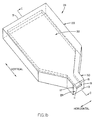
- Figure lb shows a portion of an inductive magnetic recording head 26 that can be used for writing and reading magnetic signals onto and from a magnetic recording medium.
- the portion of the recording head 26 shown includes a yoke portion 28 and a poletip portion 30.
- the yoke 28 and poletip 30, are each formed, as shown in Fig. 1b, of a laminate of a spacer layer of nonmagnetic material 11 sandwiched between two layers of magnetic material 13, 15.
- the structure 26 includes edge closure layers 17 and 19 disposed on opposed side edges of yoke 28 and on opposed side edges of poletip 30.
- the edge-closure layers 17 and 19 are comprised of magnetic material and are in magnetic contact with magnetic layers 13 and 15 thereby providing a closed magnetic flux loop from layer 13 to layer 15.
- the air bearing surface 29 and the back edge 31 may be open or edge-closed; the preferred embodiment is open for both as shown.
- Each of the layers 11, 13, 15, 17 and 19 extend continuously from the air bearing surface 29 to the backedge 31.
- the air bearing surface 29 permits the recording head to lift from the media as a result of relative motion and yet remain in intimate association therewith for reading and writing the magnetic transitions requried for the storage of data information onto the magnetic media.
- a magnetic recording head includes at least two poletips and yoke portions separated by a gap. As shown in Figure 1c, the gap is located in the space 32 between the poletips 30. Figure 1c shows a cross-section of a recording head having angled sections 34 that results in the gap 36 at the poletip being substantially smaller than the separation 36 for the coils 24 in the yoke.
- the gap 32 is filled with nonmagnetic material.
- the magnetoresistive element is placed in the gap.
- the magnetoresistive element is removed from the air bearing surface and signal flux is brought to the element with a strip of magnetic material called a fluxguide.
- a fluxguide embodiment of the present invention would be a simple edge-closed strip such as the structure 10 of Figure 1a.
- Figure 1d is an example of an MR head 21 having a yoke region 28, poletip region 30 and back closure region 23.
- An MR element 27 is recessed from the air bearing surface 29; during reading, flux is brought to the MR element through a fluxguide 33 formed of the edge-closed laminate of Figure 1a.
- the fluxguide 33 could have constant cross-section or be flared (in the same manner though not necessarily with the same dimensions) as the yoke of Figure 1b.
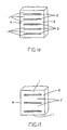
- Multilaminated embodiments of the invention are depicted in Figures 1e and 1f.
- each magnetic layer 1, separated by nonmagnetic spacers 2, and the edge-closure layers 4 and 6 are the same thickness.
- Figure 1f an embodiment is shown in which the even numbered spacers of Figure le are eliminated. In this case, the interior magnetic layers 1′ are twice as thick as the outer magnetic layers 1 and the edge-closure layers 4 and 6.
- edge closure layers of the thin film laminate of the invention act as magnetic shorts between the laterally disposed magnetic layers and have the effect of eliminating the edge-curling walls seen in prior art laminated fluxguides, yokes and poletips and also eliminating edge closure domains found in prior art unlaminated fluxguides, yokes and poletips.
- a comparison will be made of the magnetization patterns of prior art heads to the inventive recording head.
- FIGS. 2a, 2b and 2c are planar schematic depictions of prior art non-laminated inductive recording head yokes (Fig. 2a) and poletip (Figs. 2b and 2c) regions showing magnetic domain patterns.
- Triangular domains 40 (Fig. 2a) and 41 (Fig. 2b) formed along the side edges of the yoke and poletip are closure domains that form in order to minimize the total magnetic energy associated with the film in a surrounding space.
- the structure has a magnetic easy axis in the plane of the material and parallel to a recording medium 42.
- the domain walls 44 and 45 of the edge closure domains 40 and 41 are known as 90° domain walls.
- the structure further includes 180° domain walls 46 and 47 that define central domains 48 and 49.
- the arrows 50 and 51, and 52 and 53 represent the magnetic vectors for the central and edge-closure domains, respectively.
- Figure 2c represents the case where the poletip width is too narrow (for the combination of magnetic anisotropy and film thicknesses used) to form full edge-closure domains 41 and 180° walls 47.
- the edge closure domains 54 occupy a greater fraction of the film volume and the central domains 56 have a diamond shape.
- Figures 3a, 3b and 3c show the magnetization patterns of yoke and poletip regions of prior art laminated recording head structures.
- a perspective view of the laminated structure is shown in Figure 3d, which includes a layer of nonmagnetic material 58 sandwiched between two layers of magnetic material 60 and 62.
- the magnetization of the central region 65 of each of the magnetic layers 60 and 62 is in the easy axis direction as represented by arrows 64, with the flux loop being closed through the spacer 58 near the edges (arrows 67) and external fringe fields (arrows 68).
- the regions 59 in which the magnetization M curls are called edge-curling walls. M curls both between films and parallel to the films as indicated by the arrows 66 representing the surface components of the magnetization.
- edge closure domains are eliminated and are replaced by edge-curling walls depicted by arrows 55 and only one 180° domain wall 57 remains in the yoke portion; this is the lowest energy state.
- the edge-curling walls result from the rotation (curling) of the magnetic vector both in-plane and from one magnetic layer through the spacer to a second magnetic layer.
- the edge-curling walls 59 are adjacent to the upper and lower poletip edges. These regions are on the average only about half as effective in transmitting flux as the central, easy-axis, material 61.
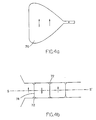
- Figure 4a shows the magnetization pattern of a yoke and poletip region of a recording head manufactured in accordance with the present invention.
- Figure 4a shows that the edge-curling walls and domain walls are completely eliminated, and there is only a single domain 70 present in both the yoke and poletip regions.
- vestigial closure domains 72 and domain wall 74 may result as shown in the poletip of Figure 4b.
- the domains 72 will be small leaving a wide channel to conduct flux by magnetization rotation; this would have essentially no effect on the read and write functions of the poletip (or fluxguide) and no significant domain noise would result.
- the actual length of the poletip is shortened such that only one or two 180° domain walls would be present in the poletip.
- Figure 5a shows in cross-section a mathematical model for a two-magnetic layer structure of the present invention.
- D The actual fabricated geometry will be more nearly rectilinear as shown in Figure 1a.
- the curved model is used to simplify the mathematics but it will be understood by those skilled in the art that the basis for the theory may be easily applied to the rectilinear case.
- Figures 5b-5e are schematic drawings of four micromagnetic states.
- Figure 5b shows the easy axis state with no leakage
- Figure 5c the easy axis state with partial leakage
- Figure 5d the hard axis state
- Figure 5e a vestigal closure domain state.
- the hard axis of anisotropy is parallel to the z axis.
- A is the exchange stiffness parameter
- K is the uniaxial anisotropy constant
- H is the stray field leaking across the nonmagnetic spacer enclosed by the magnetic film
- H is the external field having the direction z
- M s is the spontaneous magnetization.
- K K F and K C respectively.
- W F W tot - 2R2 (1.3) is the flat width, as distinguished from the total width W tot of the model.
- H km 4 ⁇ M S /( ⁇ -1) (1.6)
- FIG. 5e is a diagram of the magnetization pattern of the poletip of Figure 4b, with four sides of the tip unfolded.
- Region 75 is the planar surface shown in Figure 4b.
- Regions 76 and 77 are the edge-closed sides of the top and Region 78 is the surface opposed to Region 75 cut along the mid-line S-S′ of Figure 4b.
- Figure 6 illustrates a phase diagram predicted by the foregoing energy expressions.
- the wide line is a phase boundary.
- the narrow lines are contours of H km in the easy-axis "no leakage” phase and the angle ⁇ of the edge-curling wall in the easy-axis "partial-leakage” phase.
- the flat-film anisotropy field H kf 3 Oe is typical of what can be induced in permalloy with a field during deposition.
- the mean anisotropy field H km (Eq. (1.5) and (1.6)) throughout the preferred "no leakage" region of the phase diagram is only a little less than 3 Oe, indicating that stability against magnetostrictive effects would not be greatly diminished.
- the edge-wall angle ⁇ is small, indicating that much of this region might produce only slightly more noise than the no-leakage phase. Shorting the laminations tends to favor greater b, permitting the easy avoidance of exchange coupling through pinholes in the spacer.
- very narrow poletip regions may be fabricated and exhibit little or no domain noise.
- a successful strategy for eliminating, or at least minimizing, the presence of domain walls will depend on what device characteristics are desired and what ranges of material parameters and degrees of control are used.
- Figure 6 indicates that increasing the magnetic sublayer thickness D anywhere within the "partial leakage" region should decrease circuit noise because the wall-angle ⁇ , and therefore the noisy flux capacity of the wall, thereby decreases. However, it may be necessary to limit D to avoid signal loss at high frequency due to eddy current damping. If D had to be as small as 0.2 um, for example, there would be a trade-off between the need for small spacer thickness b for the sake of signal strength and large b for the sake of minimizing noise due to irreversible wall switching.
- a laminate 80 includes a spacer layer of nonmagnetic material 82 sandwiched between two layers of ferromagnetic material 84 and 86. Edge closure regions 88 and 90 of ferromagnetic material are provided similar to the structure of Figure 1a.
- a layer of antiferromagnetic material 92 is disposed within the structure and is in contact with magnetic layer 84 and nonmagnetic spacer layer 82, but is spaced from magnetic layer 86. The advantage of the antiferromagnetic layer will be described below.
- Figure 7b is a perspective view of an alternative embodiment of a multiple layer structure having two nonmagnetic spacers 94 and 96, each of which are sandwiched between magnetic layers 98, 100 and 102, 104, respectively.
- Edge closure layers 106 and 108 provide magnetic contact to all the magnetic layers on the side edges.
- a layer 107 of antiferromagnetic material is disposed between magnetic layers 100 and 102 to provide the additional anisotropy.
- the air bearing surface 109 is not edge-closed.
- the magnetic layers in the embodiments of Figures 7a and 7b are comprised of a ferromagnetic material.
- the side edge closure regions provide an efficient closure path between lamina, lower in energy than the external fringe field closure normally encountered between laminated films. Additional dimensional flexibility while retaining the desired easy axis state (Figure 5b) can be obtained by exchange biasing as shown in Figures 7a and 7b.
- the desired bias of the edge closed lamina can be achieved by placing an oriented antiferromagnetic film in direct contact with one lamina, but out of contact with the other by means of the nonmagnetic spacer, as shown in Fig. 7a.
- the drop off in horizontal magnetization at the two edges is no worse than that which occurs in conventionally laminated films at the edges, and can be better controlled.
- the antiferromagnetic layer 107 need not extend all the way to the air bearing surface, for example, to reduce sensitivity to corrosion and wear but may be terminated within about 1 micron of the air bearing surface.
- Figure 7c shows the air bearing surface 105 of such a structure.
- the distance that the magnetic layer 107 is recessed is not critical, and it should be pointed out that the nonmagnetic spacers 94 and 96 do extend all of the way to the air bearing surface 105. The reason for this is to ensure the circular magnetization pattern between the two pairs of magnetic layers 98, 100 and 102, 104 extends all the way to the air bearing surface.
- the magnetic thin film structures of the present invention are formed by depositing thin film layers on a substrate that may or may not be composed of a single crystal. Any of the conventional materials for the substrate may be used such as ferrites, glass and alumina.
- the magnetic material is typically a ferromagnetic material which is usually highly permeable and soft such as NiFe.
- the magnetic layers may also be formed of ferrimagnetic materials, such as MnZn ferrite.
- Permalloy is a preferred ferromagnetic material utilized for the magnetic layers of the structure, which comprises about 80% nickel and 20% iron. Other ferromagnetic materials may also be used such as supermalloy. Suitable ferrimagnetic materials include MnZn and NiZn ferrites.
- any suitable nonmagnetic material may be utilized for the spacers such as NiP, Cu, Cu alloys, Pd, Pd alloys, Al2O3 or SiO2.
- the antiferromagnetic material may be a magnesium gamma phase alloy of binary, ternary and higher level alloys with elements selected from the group consisting of Fe, Co, Cu, Ge, Ni, Pt, and Rh, with Mn. Typically, FeMn is utilized for the antiferromagnetic layer.
- the laminate can have an even number of identical magnetic layers with edge-closure layers of the same material and thickness.
- some of the magnetic layers may be of different magnetic materials, with thicknesses selected to carry the same magnetic flux in saturation.
- the fabrication of the thin film structure of the present invention utilizes processing steps well known in the electronics industry. These steps include conventional etching and masking techniques and deposition techniques. The magnetic, nonmagnetic and antiferromagnetic layers may also be deposited by conventional plating techniques.
- a substrate 110 is provided and a thin seed layer 112 of NiFe is deposited on the substrate 110.
- the seed layer 112 is overcoated with a thin plating barrier 114.
- the plating barrier must inhibit plating of permalloy on the seed layer but must be selectively etched off where plating is desired.
- 800 angstroms of SiO2 may be evaporated to form the layer 114.
- Other possible plating barriers include 200 to 400 angstroms of Ti, Ta, Nb or Si.
- a conventional photoresist plating frame 116 is deposited on the plating barrier 114.
- plating barrier 114 is then chemically etched away.
- the plating frame 116 as is conventionally known, is deposited in the shape of the structure being fabricated, such that the head will be formed from material deposited inside the frame. After deposition, all magnetic material outside the frame is removed by chemical etching.
- the drawings used herein to describe the fabrication steps are cross-sectional views.
- the laminate of alternate magnetic layers and nonmagnetic spacers is plated on the exposed regions of layer 112.
- the laminate may comprise a single nonmagnetic spacer sandwiched between two magnetic layers or may contain a multiplicity of spacers each sandwiched between two magnetic layers with the requirement that there be an "even" number of magnetic layers.
- the methods and techniques disclosed below with reference to the figures describe the fabrication of a laminate comprising a multiplicity of layers, however, it should be understood that the same techniques will be utilized for a laminate comprised of two magnetic layers and a single nonmagnetic spacer.
- intermediate layers 120 of NiFe are alternately plated with layers 126 of NiP.
- the last layer plated must be a nonmagnetic spacer so that the upper layer of the laminate is nonmagnetic material.
- Non-magnetic spacers are made sufficiently thick to minimize flux leakage as shown in Figure 6, typically 300 angstroms or greater. This loosens fabrication tolerances and eliminates concern for pinholes. Magnetic layer thickness is determined by performance requirements such as required writing flux and bit resolution.
- the plating of the magnetic and nonmagnetic layers can be out of separate baths. Alternatively, the magnetic and nonmagnetic layers may be alternately plated out of the same bath by known composition modulation plating techniques, such as that disclosed by L.T. Romankiw, J.T. Olsen, Ext. Abs. Electro. Chem. Soc., Vol. 89, Abs #300, p. 430-31, Fall 1989.
- the plating frames are removed by conventional photoresist removal techniques and a top magnetic layer 134 is then plated onto the laminate.
- plating also occurs on the edges of the laminate producing side edge closure layers 136 and 138 of magnetic material.
- the plating barrier layer 114 which remains after the plating frames are removed, prevents plating of magnetic material onto the seed layer 112.
- the thickness of the final layer 134 and side edges 136 and 138 is chosen to equal the sum of the desired NiFe thickness plus the amount that will be lost when sputter etching to remove the seed layer in later steps.
- the desired final NiFe thickness will usually be the same as (or half as thick as in Figure 1f) the underlying magnetic layers.
- a photoresist cap layer 140 is deposited to protect the entire laminate structure. All the material that was plated outside the plating frame 116 is etched away. The cap 140 is removed and as shown in Figure 8e, in phantom, the plating barrier and seed layer wings 137 and 139 are removed by reactive ion etching and sputter etching. Typically, an RIE process using CF4 is utilized to etch the SiO2. Since CF4 drastically inhibits the etching of NiFe, no significant permalloy is lost in this step. The system is then operated in the sputter etch mode with Ar to sputter etch away the NiFe seed layer.
- a substrate 142 is provided with a seed layer 144 of NiFe and photoresist frame 146.
- No plating barrier overlayer is provided in this method.
- layers 150 of magnetic material are alternately plated with spacers 158 of nonmagnetic material as disclosed above. The plating is stopped when the desired number of layers is reached with the top layer 150 being permalloy of thickness equal to that of the outer magnetic layer and edge-closure layer.
- the plating frame resist 146 is then removed as shown in Figure 9c. Additional permalloy layer 166 is then deposited on the top together with side edges 168 and 170 on the laminate.
- the top layer 166 is plated to a thickness equal to or greater than the other magnetic layers.
- Protective resist cap 172 is deposited over the laminate and the excess plating material is etched away. The resist cap is removed and the side wings 174, 176 are sputter etched as well as the thickness of layer 166 to provide the edge closed laminate. Since in sputter etching, material is removed rapidly from areas normal to the impinging ions, and either not removed or even redeposited on surfaces parallel to the ion acceleration, the plated edge closure layers 168 and 170 remain intact during sputter etching of the wings.
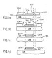
- Figures 10a-10c show another embodiment wherein edge closure is provided after the poletip and gap structure is completed.
- a first laminate 178 is deposited on a substrate 180.
- An appropriate gap layer 182 is deposited which may comprise Al2O3 which is non-conductive.
- a second laminate 184 is deposited thereby forming the two yoke regions and two poletip regions of a complete recording head.
- a resist 186 is then deposited on top of the laminate 184 at the desired width for the structure.
- the exposed regions of laminates 178 and 184 and the gap region 182 are removed by conventional trimming or ion milling techniques and the resulting structure is shown in Figure 10b.
- the exposed ion milled edges 181, 183, 185 and 187 of the laminates 178 and 184 are activated by immersing the structure in a standard palladium chloride activating solution. Subsequently, the structure is immersed in a standard electroless NiFe bath which may preferably contain DMAB as a reducing agent. As shown in Figure 10c, closure layers 188, 190, 192 and 194 are plated on the laminates 178 and 184 to form the edge closed structures.
- the immersion time of the electroless bath depends on the NiFe thickness desired on the edges. The thickness should be approximately the same as the outer magnetic layers in the laminates.
- the resist 186 is removed after the NiFe plating is completed.
- the first magnetic layer 196 is deposited on substrate 198 by conventional processes such as evaporation, sputter deposition and ion beam deposition to a thickness of typically 200 to 400 angstroms.
- Photoresist layer 200 is deposited having window 202 that defines the width of the nonmagnetic layer.
- a nonmagnetic spacer layer 204 is then deposited through the window 202 by the conventional deposition processes mentioned above.
- a refractory metal may be suitable for the spacer such as Mo, W, Ta or Ti.
- the structure is then heated, typically to 110°C for ten minutes, to cause overhang regions 206 and 208 of the photoresist masking layer 200 to shrink back thereby widening the window 202 as shown in Figure 11b. It is known that the edge of the masking layer will retract by 0.5 microns under these conditions when 100-200 angstroms of Mo has been deposited on top of the resist.
- a second magnetic layer 210 is deposited on the nonmagnetic spacer 204 also using the same deposition processes described above.
- the thickness and composition of this layer would typically be the same as that for the first magnetic layer 196, although this is not a requirement of the process.
- the second magnetic layer 210 extends beyond the edges of the spacer 204 and is in magnetic contact with the first magnetic layer 196.
- a second masking layer 212 is deposited on layer 210 to serve as a sputter etch mask for patterning the first magnetic layer.
- the second masking layer 212 may also comprise a refractory metal such as Ti, W, Ta and Mo.
- the structure is then immersed in an appropriate organic solvent to remove (lift off) the unwanted metal and the resist masking layer 200 to leave the structure shown in Figure 11c. Since the sputter etch mask 212 is defined in the same operation as the second magnetic layer 210, there is automatic registration between the two layers.
- the first magnetic layer 196 is then patterned to coincide with the second magnetic layer 210 by removing the exposed regions of the first layer 196 outside the laminate by sputter or reactive ion etching.
- the second masking layer 212 is then removed by reactive ion etching.
- Ti is a suitable material for the etch mask 212 since it etches slowly compared to NiFe in pure Ar or in Ar with five percent O2 but etches very rapidly compared to NiFe in a CF4 plasma.
- FIG 12a-c an alternative embodiment applicable where it is only desirable to provide an edge closure layer on one edge of the laminate is shown.
- a substrate 214 is provided with the first magnetic seed layer 216; a masking layer 218 having window 220 is deposited identically as described for Figure 11a. In this embodiment, however, the window 220 defines the width of the final structure.
- the deposition of the spacer 222 is performed with the structure tilted so that incident material flux depicted by arrows 224 is at an angle to an axis 226 normal to the substrate. As shown in Figure 12a, the tilt angle results in the spacer 222 being shifted to one side of the window.
- Deposition of the second magnetic layer 228, is done with normal incidence of deposition 240, as shown in Figure 12b. This results in the magnetic layer 228 being formed with one side edge closure region 230 in contact with the first magnetic layer 216 but with no edge closure layer on the opposite side of the laminate.
- the remaining steps of the process are identical to those described in the previous embodiment in which an etch mask layer 232 is deposited with the angle of deposition being parallel to the normal axis as shown in Figure 12b.
- the masking layer 218, the excess of seed layer 216 and the masking layer 232 are removed by steps similar to those discussed with Figure 11 to provide the structure shown in Figure 12c.
- the antiferromagnetic layer need only be on the order of 100-500 angstroms and does not substantially increase the total thickness of the structure.
- the exchange bias field can be kept at least twice the coercivity if the NiFe layers adjacent to the FeMn are kept less than 3600 angstroms in thickness, assuming the NiFe coercivity is 0.5 Oe.
- a structure with four NiFe layers can be effectively exchange biased with one antiferromagnetic FeMn layer as shown in Fig. 7b.
- the nonmagnetic laminating spacer layer need only be thick enough to break exchange coupling between the antiferromagnetic layer and the second NiFe lamina, for a structure like that in Fig. 7a; or between the edge-connected NiFe layers for the structure depicted in Fig. 7b.
- a thickness of 1,000-3,000 angstroms would be sufficient. It is desirable to make this nonmagnetic layer as nearly free of pinholes as possible, so as not to upset the biasing configuration.
- the antiferromagnetic bias layer does not extend all the way to the air bearing surface, because the film, in the case of FeMn, can be subject to corrosion. By choosing to terminate the antiferromagnetic film in this manner, the bias film can be totally encapsulated by the soft NiFe film, so that ambient corrosion will be the same as that of the NiFe.
- the antiferromagnetic layer horizontal magnetization orientation can be achieved in several ways: (1) deposit it in the presence of an applied field; (2) deposit it onto a previously oriented soft magnetic layer; (3) deposit it onto a previously oriented soft magnetic layer while an orienting field is also applied; (4) deposit all soft magnetic and antiferromagnetic layers (preferably in an applied orienting field), followed by a setting anneal of the structure at a temperature above or near the Neel temperature of the antiferromagnetic layer and cooling in the presence of an applied orienting field.
- the attributes of the preferred structure consist of antiferromagnetically biased, adjacent NiFe layers, with separated edge-connected NiFe layers to provide the return flux paths.
- the thicknesses of the basic layers of NiFe are preferably equal for reasons of flux-closure.
- the FeMn layers do not extend to the edges of the NiFe films, nor does it extend to the ABS.
- the nonmagnetic layers do not extend to the edges of the NiFe, except at the ABS, where it is preferable to extend the nonmagnetic material all of the way to the ABS.
- the resultant structure with its easy-axis alignment in the trackwidth direction, will have optimum rotational permeability for detecting media flux during readback.
- the domain state is stable and is determined by the antiferromagnetic biasing film, and as such, the structure will have low noise due to unwanted or extra domain wall movement.
- This structure provides a "built-in" easy axis, and so it avoids one of the potential pitfalls of simple lamination. Recording heads can be made with trackwidths in the range of a few micrometers, narrower than the current state-of-the-art.
Landscapes
- Engineering & Computer Science (AREA)
- Power Engineering (AREA)
- Chemical & Material Sciences (AREA)
- Crystallography & Structural Chemistry (AREA)
- Nanotechnology (AREA)
- Manufacturing & Machinery (AREA)
- Magnetic Heads (AREA)
Applications Claiming Priority (2)
| Application Number | Priority Date | Filing Date | Title |
|---|---|---|---|
| US432649 | 1989-11-07 | ||
| US07/432,649 US5032945A (en) | 1989-11-07 | 1989-11-07 | Magnetic thin film structures fabricated with edge closure layers |
Publications (2)
| Publication Number | Publication Date |
|---|---|
| EP0427171A2 true EP0427171A2 (de) | 1991-05-15 |
| EP0427171A3 EP0427171A3 (en) | 1991-10-30 |
Family
ID=23717033
Family Applications (1)
| Application Number | Title | Priority Date | Filing Date |
|---|---|---|---|
| EP19900121124 Ceased EP0427171A3 (en) | 1989-11-07 | 1990-11-05 | Magnetic thin film structures and methods for forming same |
Country Status (3)
| Country | Link |
|---|---|
| US (3) | US5032945A (de) |
| EP (1) | EP0427171A3 (de) |
| JP (1) | JPH03254412A (de) |
Cited By (6)
| Publication number | Priority date | Publication date | Assignee | Title |
|---|---|---|---|---|
| EP0441186A3 (en) * | 1990-02-09 | 1992-07-08 | International Business Machines Corporation | Magnetic film laminate and magnetic secondary head thereof |
| EP0656666A1 (de) * | 1993-12-03 | 1995-06-07 | Hughes Aircraft Company | Integrierter magnetoresistiever Fühler, Verfahren zu dessen Herstellung und Vorrichtung |
| EP0660127A3 (de) * | 1993-12-23 | 1996-01-17 | Ibm | Mehrschicht magnetoresistiver Fühler. |
| WO1997016823A1 (en) * | 1995-10-30 | 1997-05-09 | Philips Electronics N.V. | Magnetic head having a laminated flux guide, and device provided with the magnetic head |
| US9362491B2 (en) | 2010-03-31 | 2016-06-07 | Everspin Technologies, Inc. | Methods of manufacturing a magnetic field sensor |
| USRE46180E1 (en) * | 2009-09-25 | 2016-10-18 | Everspin Technologies, Inc. | Three axis magnetic field sensor |
Families Citing this family (75)
| Publication number | Priority date | Publication date | Assignee | Title |
|---|---|---|---|---|
| US5287237A (en) * | 1990-03-16 | 1994-02-15 | Hitachi, Ltd. | Antiferromagnetic film superior in corrosion resistance, magnetoresistance-effect element and magnetoresistance-effect head including such thin film |
| US5208715A (en) * | 1990-08-31 | 1993-05-04 | Seagate Technology, Inc. | Shield geometry for stabilizing magnetic domain structure in a magnetoresistive head |
| US5379172A (en) * | 1990-09-19 | 1995-01-03 | Seagate Technology, Inc. | Laminated leg for thin film magnetic transducer |
| US5134535A (en) * | 1991-01-18 | 1992-07-28 | Digital Equipment Corporation | Architecture for a thin-film magnetic recording head |
| DE69219936T3 (de) * | 1991-03-29 | 2008-03-06 | Kabushiki Kaisha Toshiba | Magnetowiderstandseffekt-Element |
| US5590008A (en) * | 1991-04-25 | 1996-12-31 | Hitachi, Ltd. | Magnetic disc unit having a plurality of magnetic heads which include multilayer magnetic films |
| JPH0589435A (ja) * | 1991-09-27 | 1993-04-09 | Toshiba Corp | 磁気抵抗効果型磁気ヘツド |
| US5262914A (en) * | 1991-10-18 | 1993-11-16 | International Business Machines Corporation | Magnetoresistive head with enhanced exchange bias field |
| US5314520A (en) * | 1992-02-12 | 1994-05-24 | The Furukawa Electric Co., Ltd. | Method for manufacturing optical fiber preform |
| JP2748767B2 (ja) * | 1992-03-19 | 1998-05-13 | 松下電器産業株式会社 | 薄膜磁気ヘッド及びその製造方法 |
| US5621595A (en) * | 1992-10-20 | 1997-04-15 | Cohen; Uri | Pinched-gap magnetic recording thin film head |
| US5945007A (en) * | 1992-10-20 | 1999-08-31 | Cohen; Uri | Method for etching gap-vias in a magnetic thin film head and product |
| US5385637A (en) * | 1992-12-07 | 1995-01-31 | Read-Rite Corporation | Stabilizing domains in inductive thin film heads |
| US5995339A (en) * | 1993-03-18 | 1999-11-30 | Fujitsu Limited | Magnetoresistive head with a front flux guide and an embedded MR element |
| US5392169A (en) * | 1993-06-08 | 1995-02-21 | International Business Machines Corporation | Electrical means to diminish read-back signal waveform distortion in recording heads |
| US6205007B1 (en) * | 1993-11-22 | 2001-03-20 | U.S. Philips Corporation | Thin-film magnetic head and method of manufacturing the magnetic head |
| US5559653A (en) * | 1993-12-10 | 1996-09-24 | Yamaha Corporation | Thin film magnetic head having a multilayer upper core |
| US5696654A (en) * | 1994-04-21 | 1997-12-09 | International Business Machines Corporation | Dual element magnetoresistive sensor with antiparallel magnetization directions for magnetic state stability |
| JPH0817020A (ja) * | 1994-06-30 | 1996-01-19 | Sony Corp | 磁気抵抗効果型薄膜磁気ヘッド |
| US5874886A (en) * | 1994-07-06 | 1999-02-23 | Tdk Corporation | Magnetoresistance effect element and magnetoresistance device |
| JPH08153310A (ja) * | 1994-11-28 | 1996-06-11 | Sony Corp | 磁気抵抗効果型薄膜磁気ヘッド |
| US5617278A (en) * | 1995-03-20 | 1997-04-01 | Read-Rite Corporation | Magnetic head structure with reduction of magnetic domain instability |
| US5838521A (en) * | 1995-04-17 | 1998-11-17 | Read-Rite Corporation | Magnetoresistive transducer having laminated magnetic shields |
| WO1997008687A1 (en) * | 1995-08-23 | 1997-03-06 | Hitachi, Ltd. | Magnetic head and magnetic memory apparatus using the head |
| US6011664A (en) * | 1995-08-31 | 2000-01-04 | Carnegie Mellon University | Techniques for ultrahigh density writing with a probe on erasable magnetic media |
| JPH1083517A (ja) * | 1996-09-10 | 1998-03-31 | Alps Electric Co Ltd | 薄膜磁気ヘッド及びその製造方法 |
| JP3184465B2 (ja) * | 1996-11-19 | 2001-07-09 | アルプス電気株式会社 | 薄膜磁気ヘッドおよびその製造方法 |
| US5805392A (en) * | 1996-12-30 | 1998-09-08 | Quantum Corporation | Laminated plated pole pieces for thin film magnetic transducers |
| US5867889A (en) * | 1997-04-01 | 1999-02-09 | International Business Machines Corporation | Double self-aligned insulated contiguous junction for flux-guided-MR or yoke-MR head applications |
| JPH1116122A (ja) * | 1997-06-20 | 1999-01-22 | Tdk Corp | 薄膜磁気ヘッド |
| US6222702B1 (en) | 1997-08-15 | 2001-04-24 | Seagate Technology, Inc. | Magnetic read element shield having dimensions that minimize domain wall movement |
| US6042897A (en) * | 1997-11-17 | 2000-03-28 | Alps Electric Co., Ltd. | Combination read/write thin film magnetic head and its manufacturing method |
| JP3305244B2 (ja) | 1997-12-10 | 2002-07-22 | アルプス電気株式会社 | 薄膜磁気ヘッドおよびその製造方法 |
| US6034848A (en) * | 1998-04-22 | 2000-03-07 | International Business Machines Corporation | Low profile multi-layer coil merged thin film magnetic head |
| GB9823279D0 (en) * | 1998-10-23 | 1998-12-23 | Seagate Technology | Closed edgepole design for merged magneto-resistive heads |
| US6169646B1 (en) | 1998-11-18 | 2001-01-02 | Seagate Technology, Inc. | Magnetoresistive shield incorporating seedlayer for anisotropy enhancement |
| US6097578A (en) * | 1998-12-02 | 2000-08-01 | Seagate Technology, Inc. | Bottom shield design for magnetic read heads |
| US6222707B1 (en) | 1998-12-28 | 2001-04-24 | Read-Rite Corporation | Bottom or dual spin valve having a seed layer that results in an improved antiferromagnetic layer |
| US6353511B1 (en) | 1999-06-15 | 2002-03-05 | Read-Rite Corporation | Thin film write head for improved high speed and high density recording |
| US6477009B1 (en) | 1999-07-29 | 2002-11-05 | Storage Technology Corporation | Read module with hybird closure |
| JP2001067613A (ja) * | 1999-09-01 | 2001-03-16 | Fujitsu Ltd | 磁気ヘッド作成方法 |
| US6473265B1 (en) | 1999-12-06 | 2002-10-29 | Seagate Technology Llc | High frequency writer with sliced core topology |
| US6417990B1 (en) | 1999-12-06 | 2002-07-09 | Seagate Technology Llc | Composite core structure for high efficiency writer |
| US6807031B2 (en) | 2000-02-08 | 2004-10-19 | Seagate Technology Llc | Single domain state laminated thin film structure for use as a magnetic layer of a transducing head |
| US6437949B1 (en) * | 2000-02-08 | 2002-08-20 | Seagate Technology Llc | Single domain state laminated thin film structure |
| US6453542B1 (en) * | 2000-02-28 | 2002-09-24 | Headway Technologies, Inc. | Method for fabricating balanced shield connections for noise reduction in MR/GMR read heads |
| US6972932B2 (en) * | 2000-09-06 | 2005-12-06 | Seagate Technology Llc | High-efficiency single-turn write head for high-speed recording |
| US6801409B2 (en) | 2000-09-19 | 2004-10-05 | Seagate Technology Llc | Read head shield having improved stability |
| US6989962B1 (en) | 2000-09-26 | 2006-01-24 | Western Digital (Fremont), Inc. | Inductive write head having high magnetic moment poles and low magnetic moment thin layer in the back gap, and methods for making |
| US6692898B2 (en) * | 2001-01-24 | 2004-02-17 | Infineon Technologies Ag | Self-aligned conductive line for cross-point magnetic memory integrated circuits |
| US6660412B2 (en) * | 2001-03-15 | 2003-12-09 | Waseem A. Roshen | Low loss, high frequency composite magnetic material and methods of making the same |
| US6597546B2 (en) | 2001-04-19 | 2003-07-22 | International Business Machines Corporation | Tunnel junction sensor with an antiferromagnetic (AFM) coupled flux guide |
| US6678125B2 (en) | 2002-01-11 | 2004-01-13 | International Business Machines Corporation | Enhancement of magnetization switching speed in soft ferromagnetic films through control of edge stress anisotropy |
| US7298587B2 (en) * | 2002-08-05 | 2007-11-20 | Seagate Technology Llc | Rounded top pole |
| GB2394725A (en) * | 2002-10-04 | 2004-05-05 | Qinetiq Ltd | Method of forming a magnetic information tag by electroless deposition |
| US7057837B2 (en) * | 2002-10-17 | 2006-06-06 | Hitachi Global Storage Technologies Netherlands B.V. | Flux closed single pole perpendicular head for ultra narrow track |
| US7068537B2 (en) * | 2002-11-06 | 2006-06-27 | Interuniversitair Microelektronica Centrum (Imec) | Magnetic device and method of making the same |
| US7554765B2 (en) * | 2003-06-11 | 2009-06-30 | Seagate Technology Llc | Magnetic head for perpendicular recording with suppressed side writing and erasing |
| US7295401B2 (en) * | 2004-10-27 | 2007-11-13 | Hitachi Global Storage Technologies Netherlands B.V. | Laminated side shield for perpendicular write head for improved performance |
| US7561379B2 (en) * | 2005-10-28 | 2009-07-14 | Seagate Technology Llc | Laminated return pole for suppressing side track erasure |
| US7773349B2 (en) * | 2006-02-10 | 2010-08-10 | Hitachi Global Storage Technologies Netherlands B.V. | Tunnel MR head with long stripe height sensor stabilized through the shield |
| US7768749B2 (en) * | 2006-02-10 | 2010-08-03 | Hitachi Global Storage Technologies Netherlands B.V. | Tunnel MR head with long stripe height stabilized through side-extended bias layer |
| US7630177B2 (en) * | 2006-02-14 | 2009-12-08 | Hitachi Global Storage Technologies Netherlands B.V. | Tunnel MR head with closed-edge laminated free layer |
| US7697244B2 (en) * | 2006-06-12 | 2010-04-13 | Hitachi Global Storage Technologies Netherlands B.V. | Magnetic head with stabilized ferromagnetic shield |
| US20100254830A1 (en) * | 2006-10-10 | 2010-10-07 | Beebe David J | Magnetically driven micro-pumping method using external rotating stirrer |
| US8107194B2 (en) * | 2008-09-24 | 2012-01-31 | International Business Machines Corporation | Writing and reading multi-layer continuous magnetic recording media |
| US7911739B2 (en) * | 2008-09-25 | 2011-03-22 | International Business Machines Corporation | Writing and reading multi-level patterned magnetic recording media |
| US8194360B2 (en) * | 2009-02-24 | 2012-06-05 | Seagate Technology Llc | Domain control in bottom shield of MR sensor |
| DE102009021400A1 (de) * | 2009-05-14 | 2010-11-18 | Forschungszentrum Jülich GmbH | Magnetoelektronische Bauelemente und Messverfahren |
| US8031425B2 (en) * | 2009-11-10 | 2011-10-04 | International Business Machines Corporation | Writing and reading multi-layer continuous magnetic recording media, with more than two recording layers |
| US8085502B2 (en) * | 2009-11-10 | 2011-12-27 | International Business Machines Corporation | Writing and reading multi-level patterned magnetic recording media, with more than two recording levels |
| US10784045B2 (en) * | 2015-09-15 | 2020-09-22 | International Business Machines Corporation | Laminated magnetic materials for on-chip magnetic inductors/transformers |
| US10304603B2 (en) * | 2016-06-29 | 2019-05-28 | International Business Machines Corporation | Stress control in magnetic inductor stacks |
| US10811177B2 (en) * | 2016-06-30 | 2020-10-20 | International Business Machines Corporation | Stress control in magnetic inductor stacks |
| US10283249B2 (en) | 2016-09-30 | 2019-05-07 | International Business Machines Corporation | Method for fabricating a magnetic material stack |
Family Cites Families (12)
| Publication number | Priority date | Publication date | Assignee | Title |
|---|---|---|---|---|
| US3350180A (en) * | 1967-10-31 | Magnetic device with alternating lami- na of magnetic material and non-mag- netic metal on a substrate | ||
| US4103315A (en) * | 1977-06-24 | 1978-07-25 | International Business Machines Corporation | Antiferromagnetic-ferromagnetic exchange bias films |
| AT365804B (de) * | 1977-12-20 | 1982-02-25 | Bogen Wolfgang | Abriebfester magnetkopf |
| JPS5961114A (ja) * | 1982-09-30 | 1984-04-07 | Fujitsu Ltd | 多層磁性膜の製造方法 |
| JPS5960721A (ja) * | 1982-09-30 | 1984-04-06 | Fujitsu Ltd | 薄膜型磁気ヘツド |
| JPS60256903A (ja) * | 1984-05-31 | 1985-12-18 | Matsushita Electric Ind Co Ltd | 磁気ヘツド |
| JPS60258717A (ja) * | 1984-06-04 | 1985-12-20 | Nec Corp | 薄膜磁気ヘツドおよびその製造方法 |
| US4751598A (en) * | 1985-02-01 | 1988-06-14 | Censtor Corporation | Thin-film, cross-field, closed-flux, anisotropic electromagnetic field device |
| JPS6252710A (ja) * | 1985-08-30 | 1987-03-07 | Nec Corp | 薄膜磁気ヘツド |
| US4907113A (en) * | 1987-07-29 | 1990-03-06 | Digital Equipment Corporation | Three-pole magnetic recording head |
| JPS6464108A (en) * | 1987-09-04 | 1989-03-10 | Hitachi Ltd | Magnetic head |
| JPH07114007B2 (ja) * | 1987-12-04 | 1995-12-06 | ディジタル イクイプメント コーポレーション | 記録ヘッドの積層構造磁極 |
-
1989
- 1989-11-07 US US07/432,649 patent/US5032945A/en not_active Expired - Fee Related
-
1990
- 1990-11-05 EP EP19900121124 patent/EP0427171A3/en not_active Ceased
- 1990-11-07 JP JP2299986A patent/JPH03254412A/ja active Pending
-
1991
- 1991-05-13 US US07/686,782 patent/US5331728A/en not_active Expired - Fee Related
-
1993
- 1993-12-07 US US08/163,670 patent/US5388019A/en not_active Expired - Fee Related
Cited By (19)
| Publication number | Priority date | Publication date | Assignee | Title |
|---|---|---|---|---|
| EP0441186A3 (en) * | 1990-02-09 | 1992-07-08 | International Business Machines Corporation | Magnetic film laminate and magnetic secondary head thereof |
| US5576099A (en) * | 1990-02-09 | 1996-11-19 | International Business Machines Corporation | Inductive head lamination with layer of magnetic quenching material |
| EP0656666A1 (de) * | 1993-12-03 | 1995-06-07 | Hughes Aircraft Company | Integrierter magnetoresistiever Fühler, Verfahren zu dessen Herstellung und Vorrichtung |
| US5486804A (en) * | 1993-12-03 | 1996-01-23 | Hughes Aircraft Company | Integrated magnetoresistive sensor fabrication method and apparatus |
| US5502325A (en) * | 1993-12-03 | 1996-03-26 | Hughes Aircraft Company | Integrated magnetoresistive sensor |
| EP0660127A3 (de) * | 1993-12-23 | 1996-01-17 | Ibm | Mehrschicht magnetoresistiver Fühler. |
| CN1068689C (zh) * | 1993-12-23 | 2001-07-18 | 国际商业机器公司 | 多层磁电阻检测器及其制造方法和磁存储系统 |
| WO1997016823A1 (en) * | 1995-10-30 | 1997-05-09 | Philips Electronics N.V. | Magnetic head having a laminated flux guide, and device provided with the magnetic head |
| USRE46428E1 (en) | 2009-09-25 | 2017-06-06 | Everspin Technologies, Inc. | Three axis magnetic field sensor |
| USRE46180E1 (en) * | 2009-09-25 | 2016-10-18 | Everspin Technologies, Inc. | Three axis magnetic field sensor |
| USRE49404E1 (en) | 2009-09-25 | 2023-01-31 | Everspin Technologies, Inc. | Three axis magnetic field sensor |
| USRE50684E1 (en) | 2009-09-25 | 2025-12-02 | Everspin Technologies, Inc. | Three axis magnetic field sensor |
| US9525129B2 (en) | 2010-03-31 | 2016-12-20 | Everspin Technologies, Inc. | Methods of manufacturing a magnetic field sensor |
| US9553261B2 (en) | 2010-03-31 | 2017-01-24 | Everspin Technologies, Inc. | Methods of manufacturing a magnetic field sensor |
| US9362491B2 (en) | 2010-03-31 | 2016-06-07 | Everspin Technologies, Inc. | Methods of manufacturing a magnetic field sensor |
| US9893274B2 (en) | 2010-03-31 | 2018-02-13 | Everspin Technologies, Inc. | Methods of manufacturing a magnetic field sensor |
| US10276789B2 (en) | 2010-03-31 | 2019-04-30 | Everspin Technologies, Inc. | Methods of manufacturing a magnetic field sensor |
| US11024799B2 (en) | 2010-03-31 | 2021-06-01 | Everspin Technologies, Inc. | Methods of manufacturing a magnetic field sensor |
| US11678584B2 (en) | 2010-03-31 | 2023-06-13 | Everspin Technologies, Inc. | Methods of manufacturing a magnetic field sensor |
Also Published As
| Publication number | Publication date |
|---|---|
| US5388019A (en) | 1995-02-07 |
| JPH03254412A (ja) | 1991-11-13 |
| US5331728A (en) | 1994-07-26 |
| EP0427171A3 (en) | 1991-10-30 |
| US5032945A (en) | 1991-07-16 |
Similar Documents
| Publication | Publication Date | Title |
|---|---|---|
| US5331728A (en) | Method of fabricating magnetic thin film structures with edge closure layers | |
| US5314596A (en) | Process for fabricating magnetic film recording head for use with a magnetic recording media | |
| KR100319035B1 (ko) | 박막자기헤드,기록재생분리형자기헤드,및이들을이용한자기기록재생장치 | |
| KR100225179B1 (ko) | 박막 자기 헤드 및 자기 저항 효과형 헤드 | |
| EP0472031B1 (de) | Strukturen von Dünnschichten für Magnetköpfe | |
| US6151193A (en) | Thin film magnetic head | |
| US6362940B1 (en) | Recording-reproducing magnetic head | |
| US6914761B2 (en) | Magnetoresistive sensor with magnetic flux paths surrounding non-magnetic regions of ferromagnetic material layer | |
| US6721147B2 (en) | Longitudinally biased magnetoresistance effect magnetic head and magnetic reproducing apparatus | |
| GB2387711A (en) | Magnetic sensing element with multi-layer free layer | |
| JP2001176028A (ja) | 薄膜磁気ヘッド及びその製造方法 | |
| US6327121B1 (en) | GMR head, method for its manufacture, and magnetic disc drive utilizing the head | |
| JP2001155313A (ja) | 薄膜磁気ヘッド及びその製造方法 | |
| US5761010A (en) | Magnetoresistive head, manufacturing method of the head and magnetic recording/reproducing drive | |
| US5896251A (en) | Magnetoresistance effect head with conductor film pair and magnetic field proving film pair disposed between substrate and magnetoresistance effect film | |
| US6721148B2 (en) | Magnetoresistive sensor, thin-film read/write head, and magnetic recording apparatus using the sensor | |
| JP3188232B2 (ja) | 薄膜磁気ヘッドおよびその製造方法 | |
| JP3190193B2 (ja) | 薄膜磁気ヘッドの使用方法 | |
| JPH0896328A (ja) | 磁気抵抗効果型薄膜磁気ヘッド及びその製造方法 | |
| JP2002140805A (ja) | スピンバルブ型薄膜磁気素子及び薄膜磁気ヘッド及び浮上式磁気ヘッド並びにスピンバルブ型薄膜磁気素子の製造方法 | |
| JP3939519B2 (ja) | 磁気検出素子及びその製造方法 | |
| KR100331188B1 (ko) | 박막자기헤드,기록/재생분리형헤드및이를이용한자기기록및재생장치 | |
| JP3260735B2 (ja) | 磁気抵抗効果素子、磁気抵抗効果ヘッド、および磁気記録再生装置 | |
| EP0613119B1 (de) | Magnetoresistiver Sensor und Herstellungsverfahren | |
| JP2541084B2 (ja) | 薄膜磁気ヘッド |
Legal Events
| Date | Code | Title | Description |
|---|---|---|---|
| PUAI | Public reference made under article 153(3) epc to a published international application that has entered the european phase |
Free format text: ORIGINAL CODE: 0009012 |
|
| 17P | Request for examination filed |
Effective date: 19901213 |
|
| AK | Designated contracting states |
Kind code of ref document: A2 Designated state(s): DE FR GB |
|
| PUAL | Search report despatched |
Free format text: ORIGINAL CODE: 0009013 |
|
| AK | Designated contracting states |
Kind code of ref document: A3 Designated state(s): DE FR GB |
|
| 17Q | First examination report despatched |
Effective date: 19930219 |
|
| GRAG | Despatch of communication of intention to grant |
Free format text: ORIGINAL CODE: EPIDOS AGRA |
|
| STAA | Information on the status of an ep patent application or granted ep patent |
Free format text: STATUS: THE APPLICATION HAS BEEN REFUSED |
|
| 18R | Application refused |
Effective date: 19960727 |