EP0428250A2 - Treiberschaltung für eine Anzeigetafel - Google Patents
Treiberschaltung für eine Anzeigetafel Download PDFInfo
- Publication number
- EP0428250A2 EP0428250A2 EP90309583A EP90309583A EP0428250A2 EP 0428250 A2 EP0428250 A2 EP 0428250A2 EP 90309583 A EP90309583 A EP 90309583A EP 90309583 A EP90309583 A EP 90309583A EP 0428250 A2 EP0428250 A2 EP 0428250A2
- Authority
- EP
- European Patent Office
- Prior art keywords
- bias
- circuit
- common
- output
- driver circuit
- Prior art date
- Legal status (The legal status is an assumption and is not a legal conclusion. Google has not performed a legal analysis and makes no representation as to the accuracy of the status listed.)
- Granted
Links
- 239000004973 liquid crystal related substance Substances 0.000 claims abstract description 17
- 230000000717 retained effect Effects 0.000 claims description 3
- 238000001514 detection method Methods 0.000 claims description 2
- 239000003990 capacitor Substances 0.000 abstract description 20
- 238000010276 construction Methods 0.000 abstract description 9
- 238000010586 diagram Methods 0.000 description 13
- 230000001360 synchronised effect Effects 0.000 description 5
- 101100117236 Drosophila melanogaster speck gene Proteins 0.000 description 2
- 238000012986 modification Methods 0.000 description 2
- 230000004048 modification Effects 0.000 description 2
- 230000002411 adverse Effects 0.000 description 1
- 230000003321 amplification Effects 0.000 description 1
- 230000000694 effects Effects 0.000 description 1
- 238000009499 grossing Methods 0.000 description 1
- 238000000034 method Methods 0.000 description 1
- 238000003199 nucleic acid amplification method Methods 0.000 description 1
- 230000000737 periodic effect Effects 0.000 description 1
Images


Classifications
-
- G—PHYSICS
- G09—EDUCATION; CRYPTOGRAPHY; DISPLAY; ADVERTISING; SEALS
- G09G—ARRANGEMENTS OR CIRCUITS FOR CONTROL OF INDICATING DEVICES USING STATIC MEANS TO PRESENT VARIABLE INFORMATION
- G09G3/00—Control arrangements or circuits, of interest only in connection with visual indicators other than cathode-ray tubes
- G09G3/20—Control arrangements or circuits, of interest only in connection with visual indicators other than cathode-ray tubes for presentation of an assembly of a number of characters, e.g. a page, by composing the assembly by combination of individual elements arranged in a matrix no fixed position being assigned to or needed to be assigned to the individual characters or partial characters
- G09G3/34—Control arrangements or circuits, of interest only in connection with visual indicators other than cathode-ray tubes for presentation of an assembly of a number of characters, e.g. a page, by composing the assembly by combination of individual elements arranged in a matrix no fixed position being assigned to or needed to be assigned to the individual characters or partial characters by control of light from an independent source
- G09G3/36—Control arrangements or circuits, of interest only in connection with visual indicators other than cathode-ray tubes for presentation of an assembly of a number of characters, e.g. a page, by composing the assembly by combination of individual elements arranged in a matrix no fixed position being assigned to or needed to be assigned to the individual characters or partial characters by control of light from an independent source using liquid crystals
- G09G3/3611—Control of matrices with row and column drivers
- G09G3/3648—Control of matrices with row and column drivers using an active matrix
- G09G3/3655—Details of drivers for counter electrodes, e.g. common electrodes for pixel capacitors or supplementary storage capacitors
-
- G—PHYSICS
- G09—EDUCATION; CRYPTOGRAPHY; DISPLAY; ADVERTISING; SEALS
- G09G—ARRANGEMENTS OR CIRCUITS FOR CONTROL OF INDICATING DEVICES USING STATIC MEANS TO PRESENT VARIABLE INFORMATION
- G09G3/00—Control arrangements or circuits, of interest only in connection with visual indicators other than cathode-ray tubes
- G09G3/20—Control arrangements or circuits, of interest only in connection with visual indicators other than cathode-ray tubes for presentation of an assembly of a number of characters, e.g. a page, by composing the assembly by combination of individual elements arranged in a matrix no fixed position being assigned to or needed to be assigned to the individual characters or partial characters
- G09G3/34—Control arrangements or circuits, of interest only in connection with visual indicators other than cathode-ray tubes for presentation of an assembly of a number of characters, e.g. a page, by composing the assembly by combination of individual elements arranged in a matrix no fixed position being assigned to or needed to be assigned to the individual characters or partial characters by control of light from an independent source
- G09G3/36—Control arrangements or circuits, of interest only in connection with visual indicators other than cathode-ray tubes for presentation of an assembly of a number of characters, e.g. a page, by composing the assembly by combination of individual elements arranged in a matrix no fixed position being assigned to or needed to be assigned to the individual characters or partial characters by control of light from an independent source using liquid crystals
- G09G3/3611—Control of matrices with row and column drivers
- G09G3/3648—Control of matrices with row and column drivers using an active matrix
Definitions
- the present invention generally relates to a common driver circuit for driving a load heavy in a capacitive property such as a common electrode or the like of a liquid crystal panel.
- a common driver circuit built into the conventional liquid crystal display apparatus of this type fed a bias through a variable resistor (2) to a buffer amplifier (1) to which a common amplitude signal (frame pulse) (FP) was inputted, the amplitude of the common amplitude signal was adjusted by the adjustment of the bias as shown in Fig. 6.
- the output of the buffer amplifier (1) was adapted to be removed in the direct current component by a capacitor for direct current cutting use (C1) and the common bias was adapted to be given newly by a variable resistor (3).
- C1 capacitor for direct current cutting use
- the voltage for deciding the bias may be taken from the power line the same as the source power voltage of the panel, even the bias to be set by 3 varies in the same direction in accordance with the variation if the source power voltage receives the variation, with a disadvantage that the direct current is hard to be applied upon the panel.
- both the variation in the central voltage of the video signal to be applied upon the source driver and the variation in the central voltage of the common were required to be controlled even in the conditions of the signal content, the power variation and so on.
- the feedback was already applied and was stable, while in the common, the speck was not necessarily observed because of the above described causes.
- the present invention has been developed with a view to substantially eliminating the above described drawbacks and has for its object to provide a common driver circuit, which is capable of feeding the common output provided with the stable bias, with no variation being provided in the common bias, and the capacitor of large capacity for direct current cutting use being not required.
- the present invention is composed of, in a common driver circuit for driving a liquid crystal panel, an output circuit composed of a buffer amplifier capable of sufficiently driving the capacitive load or of a voltage follower, a means for feeding the common signal and the common bias to the above described output circuit, a bias setting means for setting the above described common bias, a control means which detects the direct current level of the above described output circuit, so that the common bias set by the above described bias setting means may be normally retained through the use of the detection output.
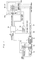
- Fig. 1 is a block diagram showing the whole construction of a liquid crystal display apparatus into which a common driver circuit has been built in.
- Fig. 2 is a block diagram of a common driver circuit shown as one embodiment of the present invention.
- Fig. 3 is a circuit diagram showing the concrete circuit construction of the respective blocks of Fig. 2.
- Fig. 4 is a signal wave form chart of the signals in each portion of Fig. 1 and Fig. 3.
- a LCD panel 40 composed of a TFT array (Thin ⁇ Film ⁇ Transistor ⁇ Array) is provided with a gate driver 40a, a source driver 40b, and a common driver 39 so as to input a gate driver driving signal into a gate driver 40a from a liquid crystal panel controller 38, a source driver driving signal into the source driver 40b, and a signal for common signal making use into the common driver 39.
- a gate driver 40a Thin ⁇ Film ⁇ Transistor ⁇ Array
- a video signal is inputted into a synchronous detaching circuit 31 and a Y/C detaching circuit 33.
- the synchronous signal which has been synchronously detached in the synchronous detaching circuit 31 is inserted into a liquid crystal panel controller 38 and a clamp pulse.
- generator 32 in a sine wave-form of 10MHz or more as shown in Fig. 4 (a).
- a Y/C detaching circuit 33 the video signal is detached into a brilliance signal and a cross signal and is inputted into a video cross signal processing circuit 34.
- Prime color signals of R, G, B are outputted from the video cross signal processing circuit 34 and are inputted into a brightness, contrast, gamma correcting circuit 35.
- the clamp pulse of a clamp pulse ⁇ generator 32 is inputted into the video cross signal processing circuit 34 and the brightness, contrast, gamma correcting circuit 35.
- the prime color signals R, G, B of the brightness, contrast, gamma correcting circuit 35 are processed in a inverter circuit 36, and are inputted into the source driver circuit 40b as the video signal output from a driver circuit 37.
- a liquid crystal panel controller 38 inputs a synchronizing signal from a synchronous detaching circuit 31, and also, inputs a clock pulse ck, outputs a gate driver driving signal and a source driver driving signal as a control signal of a panel.
- a frame pulse (FP) synchronized with the signal or an inversion pulse such a signal for common signal making use which is a horizontal periodic signal of 0 through 5V of 15MHz is outputted.
- the inversion pulse to be outputted from the liquid crystal panel controller 38 is inputted into an inverter 36 and a common driver 39.
- a horizontal periodic signal of 15KHz, which has a DC level of 0 through 5V as shown in Fig. 4 (b) as an inversion inputted into the common diver 39 is inputted into a buffer amplifier 11 as a common amplitude signal from a terminal 10 shown in Fig. 2.
- a control portion (12) for controlling bias, amplitude is connected with the buffer amplifier (11).
- the control portion (12) gives a set value established by an amplitude variable volume (13) to the buffer amplifier (11), and also, compares a bias set by a bias variable volume (14) with a direct current level feedbacked from the output circuit side by a comparator so as to vary the bias by the comparison output to give it to the buffer amplifier (11).
- the output from the above described buffer amplifier (11) is fed into the (+) input terminal as a pulse signal having a DC level of -1V through -7 with such -4V as shown in Fig. 4 (c) being provided as a center bias.
- the output of the operational amplifier (15) is connected in transistors (Q1), (Q2) for buffer use as shown so that the load heavy in the capacitive property may be sufficiently driven, with the voltage feedback being effected from the output point (a) to the (-) input terminal.
- the operational amplifier (15) and the buffer amplifiers (Q1), (Q2) compose a voltage follower 18.
- the voltage follower constitutes an output circuit (18), the output point (a) is connected with the common electrode of the liquid crystal panel, and the output is fed as a pulse signal which has a DC level of -1V through -7V with -4V being provided as a center bias as shown in Fig. 4 (d).
- a low-pass filter (16) composed of a resistor (R1) and a capacitor (C1).
- the output of the low-pass filter (16) is fed into the above described control portion (12) through a feedback circuit (17) as a signal of -4V as shown in Fig. 4 (e).
- the feedback circuit (17) is composed of an operational amplifier, with the output of the above described low-pass (16) being applied upon the plus input terminal, the voltage Vcc/2 whose power voltage + Vcc is divided in voltage by 1/2 being applied upon the minus input terminal.
- the output of the feedback circuit (17) is combined, as a signal of the -4V shown as shown in Fig. 4 (f), with one input terminal of the first, second comparators (20, 21 of Fig.
- the direct current voltage set by the bias variable volume (14) is given to the other input terminal of the comparator.
- the output of the comparator controls the bias to be given to the buffer amplifier (11) so that the direct current voltage to be given through the feedback circuit (17) from the above described low-pass filter (16) may conform to the direct current voltage from the above described bias variable volume (14) as a pulse signal varied by the VR (13), (14) in both the DC level and the amplitude as shown in Fig. 4 (g).
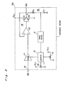
- the block diagram of Fig. 2 is concretely composed of a circuit diagram shown in Fig. 3.
- the buffer amplifier 11 is composed of a working amplifier 19 and resistors R1, R2, R3, R4.
- the voltage follower 18 is composed of the operational amplifier 15 and a pair of transistors Q1, Q2 for buffer use.
- the feedback circuit 17 is composed of a working amplifier 17 and a resistor R6.
- the low-pass filter circuit 16 is composed of a resistor R1 and a capacitor C1, with the direct current component thereof being inputted into the working amplifier of the feedback circuit 17.
- the feedback circuit 17 is composed of a working amplifier 22 and a resistor R6, with the output thereof being inputted into a first comparator 20 and a second comparator 21 of the control portion (12).
- the control portion 12 is composed of a first comparator 20, a second comparator 21, resistors R7, R8, R9, R10 and a capacitor C2.
- the amplitude variable volume (13) connected with the first comparator 21 is to adjust the amplitude of the output signal from the control portion (12).
- the bias variable volume 14 connected with the second comparator 20 is to adjust the center bias of the output signal from the control portion (12).
- the inversion pulse inputted from the terminal (10) is amplified (or contracted) by the control signal from the control portion of the control portion (12) by the circuit 11, and at the same time, the bias is also controlled.
- the control signal of the bias to be made by the amplification circuit (12) is made through the comparison by the feedback circuit (17) between a reference level set by the bias variable volume (14) and a level of a signal to be made by the low-pass filter (16).
- the amplifier of the circuit (11) is controlled so that the output of the voltage follower (18) may become normally constant.
- the capacitor C3 together with the resistor R6 is provided for the smoothing use.
- the inversion pulse inputted into the common driver 39 is adapted to be added into the liquid crystal panel LCD, with the amplitude stabilized by the concrete circuit of Fig. 3 and the bias being set.
- the common driver circuit in accordance with the present invention is composed of a block circuit as shown in Fig. 2, and may be constructed as in the circuit diagram of Fig. 5 as a modified example in addition to the concrete circuit in Fig. 3.
- the inversion pulse supplied to the input terminal (51) is inputted into the operational amplifier (52).
- the amplitude of the inputted inversion pulse is adjusted by the variable feedback resistor (53).
- the output of the amplifier (52) is inputted into the voltage follower (54) and is taken out as the common output.
- the common output is taken out as the direct current output by the low pass filter composed of the resistor R17, and capacitor C12, and is inputted into the comparator (56).
- the level set by the comparator (57) and variable resistor (58) is compared with the above described low-pass filter output level, and the comparator output is applied to the voltage follower (55) through the low-pass filter comprising the resistor R18 and capacitor C13.
- the output is applied to the amplifier (52) so that the output of the low-pass filter comprising the resistor R17 and the capacitor C12 may become normally a level set by the variable resistor (58) with the direct current as shown in Fig. 4 (g).
- the capacitor C11 of Fig. 5 is provided for the by-pass (especially when the higher frequency is handled) of the high frequency component.
- the capacitor C13 smooths the output of the comparator (56), which drops to the reference voltage (the output of the (57)).
- the capacitor C14 provides protection against noise.
- the common output is smoothed by the resistor R17, the capacitor C12, and is inputted into the comparator (56).
- the bias set VR of the potentiometer (58) is established using both Vcc, Vee from the same power line as the source power voltage of the panel.
- the bias to be set by the potentiometer (58) sets the bias of the common output, and also, becomes a reference voltage of the direct current feedback, so that it may follow even the variation in the source power voltage.
- the variation in the voltage to be applied upon the panel becomes smaller because of the movement in accordance with the variation in the reference voltage. Since the circuits are all directly connected in construction, the capacitor for the direct current cutting use is not required.
- the modified example of Fig. 5 provides the same effect as that of Fig. 3, with the stability that the feedback resistor (53) is varied with the volume in the amplitude adjustment.
- the common driver circuit in accordance with the present invention is composed of the simple circuit construction provided with each of voltage follower, low-pass filter, feedback and control circuits.
- the variation in the direction current component which adversely affects the signal processing of this type of circuit is inhibited so as to improve reliability.
- D.C. cutting at the front end of the output circuit for providing a common bias is not required, so that a large capacity direct current cutting capacitor becomes unnecessary.
Landscapes
- Engineering & Computer Science (AREA)
- Chemical & Material Sciences (AREA)
- Crystallography & Structural Chemistry (AREA)
- Physics & Mathematics (AREA)
- Computer Hardware Design (AREA)
- General Physics & Mathematics (AREA)
- Theoretical Computer Science (AREA)
- Power Engineering (AREA)
- Liquid Crystal Display Device Control (AREA)
- Transmitters (AREA)
Applications Claiming Priority (4)
| Application Number | Priority Date | Filing Date | Title |
|---|---|---|---|
| JP102406/89 | 1989-08-31 | ||
| JP10240689 | 1989-08-31 | ||
| JP2215496A JP2587526B2 (ja) | 1989-08-31 | 1990-08-14 | コモンドライバー回路 |
| JP215496/90 | 1990-08-14 |
Publications (3)
| Publication Number | Publication Date |
|---|---|
| EP0428250A2 true EP0428250A2 (de) | 1991-05-22 |
| EP0428250A3 EP0428250A3 (en) | 1992-07-01 |
| EP0428250B1 EP0428250B1 (de) | 1995-10-25 |
Family
ID=26443125
Family Applications (1)
| Application Number | Title | Priority Date | Filing Date |
|---|---|---|---|
| EP90309583A Expired - Lifetime EP0428250B1 (de) | 1989-08-31 | 1990-08-31 | Treiberschaltung für eine Anzeigetafel |
Country Status (5)
| Country | Link |
|---|---|
| EP (1) | EP0428250B1 (de) |
| CN (1) | CN1021605C (de) |
| AU (1) | AU623802B2 (de) |
| ES (1) | ES2078316T3 (de) |
| MY (1) | MY109311A (de) |
Cited By (8)
| Publication number | Priority date | Publication date | Assignee | Title |
|---|---|---|---|---|
| EP0606763A1 (de) * | 1992-12-28 | 1994-07-20 | Sharp Kabushiki Kaisha | Treiberschaltung für gemeinsame Elektrode zur Verwendung in einem Anzeigegerät |
| EP0572079A3 (en) * | 1992-05-28 | 1994-08-10 | Philips Electronics Uk Ltd | Liquid crystal display devices |
| EP0570001A3 (de) * | 1992-05-14 | 1994-11-30 | Toshiba Kk | Flüssigkristallanzeigegerät. |
| EP0558060A3 (de) * | 1992-02-28 | 1995-07-05 | Canon Kk | |
| EP0682842A4 (de) * | 1992-11-24 | 1996-03-13 | Hughes Jvc Tech Corp | Vorspannungstreiber und rauschreduzierung in bildprojektoren. |
| EP0735520A1 (de) * | 1995-03-31 | 1996-10-02 | Sharp Kabushiki Kaisha | Helligkeitsregelung in einer Flüssigkristallanzeigeeinrichtung mit Kompensation der Nichtlinearität |
| US5892504A (en) * | 1991-07-17 | 1999-04-06 | U.S. Philips Corporation | Matrix display device and its method of operation |
| US9715856B2 (en) | 2013-12-24 | 2017-07-25 | Boe Technology Group Co., Ltd. | Common voltage adjustment circuit for display panel and display apparatus |
Families Citing this family (5)
| Publication number | Priority date | Publication date | Assignee | Title |
|---|---|---|---|---|
| EP1532611B1 (de) * | 2002-08-21 | 2015-09-09 | Koninklijke Philips N.V. | Anzeigeeinrichtung |
| JP4366914B2 (ja) * | 2002-09-25 | 2009-11-18 | 日本電気株式会社 | 表示装置用駆動回路及びそれを用いた表示装置 |
| CN100485464C (zh) * | 2005-12-28 | 2009-05-06 | 启萌科技有限公司 | 液晶显示面板及其液晶显示装置 |
| CN103065594B (zh) * | 2012-12-14 | 2017-04-12 | 深圳市华星光电技术有限公司 | 一种数据驱动电路、液晶显示装置及一种驱动方法 |
| US9135882B2 (en) | 2012-12-14 | 2015-09-15 | Shenzhen China Star Optoelectronics Technology Co., Ltd | Data driver circuit having compensation module, LCD device and driving method |
Family Cites Families (2)
| Publication number | Priority date | Publication date | Assignee | Title |
|---|---|---|---|---|
| KR900005489B1 (ko) * | 1984-04-26 | 1990-07-30 | 마쯔시다덴기산교 가부시기가이샤 | 액정표시장치의 구동회로 |
| WO1987002537A1 (fr) * | 1985-10-16 | 1987-04-23 | Sanyo Electric Co., Ltd. | Dispositif d'affichage a cristaux liquides |
-
1990
- 1990-08-24 AU AU61324/90A patent/AU623802B2/en not_active Expired
- 1990-08-30 MY MYPI90001494A patent/MY109311A/en unknown
- 1990-08-31 EP EP90309583A patent/EP0428250B1/de not_active Expired - Lifetime
- 1990-08-31 ES ES90309583T patent/ES2078316T3/es not_active Expired - Lifetime
- 1990-08-31 CN CN90107443A patent/CN1021605C/zh not_active Expired - Lifetime
Cited By (14)
| Publication number | Priority date | Publication date | Assignee | Title |
|---|---|---|---|---|
| US5892504A (en) * | 1991-07-17 | 1999-04-06 | U.S. Philips Corporation | Matrix display device and its method of operation |
| EP0558060A3 (de) * | 1992-02-28 | 1995-07-05 | Canon Kk | |
| US5748171A (en) * | 1992-02-28 | 1998-05-05 | Canon Kabushiki Kaisha | Liquid crystal display |
| US5646643A (en) * | 1992-05-14 | 1997-07-08 | Kabushiki Kaisha Toshiba | Liquid crystal display device |
| US5434599A (en) * | 1992-05-14 | 1995-07-18 | Kabushiki Kaisha Toshiba | Liquid crystal display device |
| US5619221A (en) * | 1992-05-14 | 1997-04-08 | Kabushiki Kaisha Toshiba | Liquid crystal display device |
| EP0570001A3 (de) * | 1992-05-14 | 1994-11-30 | Toshiba Kk | Flüssigkristallanzeigegerät. |
| EP0572079A3 (en) * | 1992-05-28 | 1994-08-10 | Philips Electronics Uk Ltd | Liquid crystal display devices |
| EP0682842A4 (de) * | 1992-11-24 | 1996-03-13 | Hughes Jvc Tech Corp | Vorspannungstreiber und rauschreduzierung in bildprojektoren. |
| US5537129A (en) * | 1992-12-28 | 1996-07-16 | Sharp Kabushiki Kaisha | Common electrode driving circuit for use in a display apparatus |
| EP0606763A1 (de) * | 1992-12-28 | 1994-07-20 | Sharp Kabushiki Kaisha | Treiberschaltung für gemeinsame Elektrode zur Verwendung in einem Anzeigegerät |
| EP0735520A1 (de) * | 1995-03-31 | 1996-10-02 | Sharp Kabushiki Kaisha | Helligkeitsregelung in einer Flüssigkristallanzeigeeinrichtung mit Kompensation der Nichtlinearität |
| US5751267A (en) * | 1995-03-31 | 1998-05-12 | Sharp Kabushiki Kaisha | Liquid crystal display device |
| US9715856B2 (en) | 2013-12-24 | 2017-07-25 | Boe Technology Group Co., Ltd. | Common voltage adjustment circuit for display panel and display apparatus |
Also Published As
| Publication number | Publication date |
|---|---|
| EP0428250A3 (en) | 1992-07-01 |
| ES2078316T3 (es) | 1995-12-16 |
| CN1021605C (zh) | 1993-07-14 |
| CN1050298A (zh) | 1991-03-27 |
| MY109311A (en) | 1997-01-31 |
| AU6132490A (en) | 1991-08-01 |
| EP0428250B1 (de) | 1995-10-25 |
| AU623802B2 (en) | 1992-05-21 |
Similar Documents
| Publication | Publication Date | Title |
|---|---|---|
| US5283477A (en) | Common driver circuit | |
| EP0428250A2 (de) | Treiberschaltung für eine Anzeigetafel | |
| JPH08286169A (ja) | 液晶表示装置の対向電極調整回路 | |
| KR19980086741A (ko) | 자동 이득 제어를 위한 개선된 피크 검출기 | |
| US6412347B1 (en) | Angle speed sensor | |
| KR930011105B1 (ko) | 공통 드라이버회로 | |
| KR100229622B1 (ko) | 액정표시장치의 크로스-토크 보상회로 | |
| US5557239A (en) | Direct current offset compensating circuit of an audio system | |
| CN110658773B (zh) | 一种机器人急停控制电路 | |
| KR101186005B1 (ko) | 액정표시장치 및 그의 구동 방법 | |
| JP2895306B2 (ja) | 映像出力回路 | |
| US4845412A (en) | Speed control apparatus for motor | |
| JPH0546112A (ja) | 液晶駆動回路 | |
| JPH11126048A (ja) | 液晶パネル駆動回路 | |
| US5933198A (en) | Comb filter arrangement | |
| JP3043178B2 (ja) | 液晶電源回路 | |
| JP2930799B2 (ja) | 映像出力回路 | |
| KR910003674Y1 (ko) | 오토 센터링 회로 | |
| JP3901938B2 (ja) | ビデオagc回路 | |
| JP2001004975A (ja) | 液晶表示方法および装置 | |
| KR920000844Y1 (ko) | 음향기기의 3단 자동 레벨 조절회로 | |
| JPH08228120A (ja) | レベル信号回路 | |
| JPS63209186A (ja) | 圧電型駆動装置 | |
| JPS61161010A (ja) | 帰還型増幅器 | |
| JPH042270A (ja) | クランプ回路 |
Legal Events
| Date | Code | Title | Description |
|---|---|---|---|
| PUAI | Public reference made under article 153(3) epc to a published international application that has entered the european phase |
Free format text: ORIGINAL CODE: 0009012 |
|
| 17P | Request for examination filed |
Effective date: 19900921 |
|
| AK | Designated contracting states |
Kind code of ref document: A2 Designated state(s): DE ES FR GB |
|
| PUAL | Search report despatched |
Free format text: ORIGINAL CODE: 0009013 |
|
| AK | Designated contracting states |
Kind code of ref document: A3 Designated state(s): DE ES FR GB |
|
| 17Q | First examination report despatched |
Effective date: 19940103 |
|
| GRAA | (expected) grant |
Free format text: ORIGINAL CODE: 0009210 |
|
| AK | Designated contracting states |
Kind code of ref document: B1 Designated state(s): DE ES FR GB |
|
| REF | Corresponds to: |
Ref document number: 69023203 Country of ref document: DE Date of ref document: 19951130 |
|
| ET | Fr: translation filed | ||
| REG | Reference to a national code |
Ref country code: ES Ref legal event code: FG2A Ref document number: 2078316 Country of ref document: ES Kind code of ref document: T3 |
|
| PLBE | No opposition filed within time limit |
Free format text: ORIGINAL CODE: 0009261 |
|
| STAA | Information on the status of an ep patent application or granted ep patent |
Free format text: STATUS: NO OPPOSITION FILED WITHIN TIME LIMIT |
|
| 26N | No opposition filed | ||
| REG | Reference to a national code |
Ref country code: GB Ref legal event code: IF02 |
|
| PGFP | Annual fee paid to national office [announced via postgrant information from national office to epo] |
Ref country code: FR Payment date: 20090814 Year of fee payment: 20 Ref country code: ES Payment date: 20090827 Year of fee payment: 20 |
|
| PGFP | Annual fee paid to national office [announced via postgrant information from national office to epo] |
Ref country code: GB Payment date: 20090826 Year of fee payment: 20 Ref country code: DE Payment date: 20090827 Year of fee payment: 20 |
|
| REG | Reference to a national code |
Ref country code: GB Ref legal event code: PE20 Expiry date: 20100830 |
|
| REG | Reference to a national code |
Ref country code: ES Ref legal event code: FD2A Effective date: 20100901 |
|
| PG25 | Lapsed in a contracting state [announced via postgrant information from national office to epo] |
Ref country code: GB Free format text: LAPSE BECAUSE OF EXPIRATION OF PROTECTION Effective date: 20100830 |
|
| PG25 | Lapsed in a contracting state [announced via postgrant information from national office to epo] |
Ref country code: DE Free format text: LAPSE BECAUSE OF EXPIRATION OF PROTECTION Effective date: 20100831 |