EP0430086A2 - Transistor bipolaire à hétérojonction et son procédé de fabrication - Google Patents
Transistor bipolaire à hétérojonction et son procédé de fabrication Download PDFInfo
- Publication number
- EP0430086A2 EP0430086A2 EP90122345A EP90122345A EP0430086A2 EP 0430086 A2 EP0430086 A2 EP 0430086A2 EP 90122345 A EP90122345 A EP 90122345A EP 90122345 A EP90122345 A EP 90122345A EP 0430086 A2 EP0430086 A2 EP 0430086A2
- Authority
- EP
- European Patent Office
- Prior art keywords
- semiconductor layer
- electrode
- emitter
- transistor
- conductivity type
- Prior art date
- Legal status (The legal status is an assumption and is not a legal conclusion. Google has not performed a legal analysis and makes no representation as to the accuracy of the status listed.)
- Withdrawn
Links
- 125000005842 heteroatom Chemical group 0.000 title claims abstract description 8
- 238000004519 manufacturing process Methods 0.000 title claims description 6
- 238000005530 etching Methods 0.000 claims abstract description 20
- 238000009413 insulation Methods 0.000 claims abstract description 18
- 239000004065 semiconductor Substances 0.000 claims description 62
- 238000000034 method Methods 0.000 claims description 30
- 239000000758 substrate Substances 0.000 claims description 11
- 229910001218 Gallium arsenide Inorganic materials 0.000 claims description 10
- 150000001875 compounds Chemical class 0.000 claims 16
- 239000000463 material Substances 0.000 claims 6
- 238000000059 patterning Methods 0.000 abstract 1
- VYPSYNLAJGMNEJ-UHFFFAOYSA-N Silicium dioxide Chemical compound O=[Si]=O VYPSYNLAJGMNEJ-UHFFFAOYSA-N 0.000 description 36
- 229910052681 coesite Inorganic materials 0.000 description 18
- 229910052906 cristobalite Inorganic materials 0.000 description 18
- 239000000377 silicon dioxide Substances 0.000 description 18
- 235000012239 silicon dioxide Nutrition 0.000 description 18
- 229910052682 stishovite Inorganic materials 0.000 description 18
- 229910052905 tridymite Inorganic materials 0.000 description 18
- 229910000530 Gallium indium arsenide Inorganic materials 0.000 description 10
- 239000007789 gas Substances 0.000 description 8
- 238000001259 photo etching Methods 0.000 description 7
- 229920002120 photoresistant polymer Polymers 0.000 description 7
- 229910045601 alloy Inorganic materials 0.000 description 5
- 239000000956 alloy Substances 0.000 description 5
- 238000001020 plasma etching Methods 0.000 description 5
- 229910000980 Aluminium gallium arsenide Inorganic materials 0.000 description 3
- 238000003486 chemical etching Methods 0.000 description 3
- 230000000694 effects Effects 0.000 description 3
- 230000003071 parasitic effect Effects 0.000 description 3
- 238000000992 sputter etching Methods 0.000 description 3
- 238000007740 vapor deposition Methods 0.000 description 3
- XPDWGBQVDMORPB-UHFFFAOYSA-N Fluoroform Chemical compound FC(F)F XPDWGBQVDMORPB-UHFFFAOYSA-N 0.000 description 2
- 239000000969 carrier Substances 0.000 description 2
- 239000004020 conductor Substances 0.000 description 2
- 230000005684 electric field Effects 0.000 description 2
- 230000010354 integration Effects 0.000 description 2
- 238000004544 sputter deposition Methods 0.000 description 2
- VZGDMQKNWNREIO-UHFFFAOYSA-N tetrachloromethane Chemical compound ClC(Cl)(Cl)Cl VZGDMQKNWNREIO-UHFFFAOYSA-N 0.000 description 2
- 229910052581 Si3N4 Inorganic materials 0.000 description 1
- 239000012298 atmosphere Substances 0.000 description 1
- 125000004429 atom Chemical group 0.000 description 1
- 230000015572 biosynthetic process Effects 0.000 description 1
- 239000000470 constituent Substances 0.000 description 1
- 238000000151 deposition Methods 0.000 description 1
- PXBRQCKWGAHEHS-UHFFFAOYSA-N dichlorodifluoromethane Chemical compound FC(F)(Cl)Cl PXBRQCKWGAHEHS-UHFFFAOYSA-N 0.000 description 1
- 235000019404 dichlorodifluoromethane Nutrition 0.000 description 1
- 239000002019 doping agent Substances 0.000 description 1
- 238000001312 dry etching Methods 0.000 description 1
- 239000011521 glass Substances 0.000 description 1
- 238000010438 heat treatment Methods 0.000 description 1
- 238000002488 metal-organic chemical vapour deposition Methods 0.000 description 1
- 239000012299 nitrogen atmosphere Substances 0.000 description 1
Images

Classifications
-
- H—ELECTRICITY
- H10—SEMICONDUCTOR DEVICES; ELECTRIC SOLID-STATE DEVICES NOT OTHERWISE PROVIDED FOR
- H10D—INORGANIC ELECTRIC SEMICONDUCTOR DEVICES
- H10D10/00—Bipolar junction transistors [BJT]
- H10D10/80—Heterojunction BJTs
- H10D10/821—Vertical heterojunction BJTs
-
- H—ELECTRICITY
- H10—SEMICONDUCTOR DEVICES; ELECTRIC SOLID-STATE DEVICES NOT OTHERWISE PROVIDED FOR
- H10D—INORGANIC ELECTRIC SEMICONDUCTOR DEVICES
- H10D62/00—Semiconductor bodies, or regions thereof, of devices having potential barriers
- H10D62/10—Shapes, relative sizes or dispositions of the regions of the semiconductor bodies; Shapes of the semiconductor bodies
- H10D62/13—Semiconductor regions connected to electrodes carrying current to be rectified, amplified or switched, e.g. source or drain regions
- H10D62/133—Emitter regions of BJTs
- H10D62/136—Emitter regions of BJTs of heterojunction BJTs
-
- H—ELECTRICITY
- H10—SEMICONDUCTOR DEVICES; ELECTRIC SOLID-STATE DEVICES NOT OTHERWISE PROVIDED FOR
- H10D—INORGANIC ELECTRIC SEMICONDUCTOR DEVICES
- H10D62/00—Semiconductor bodies, or regions thereof, of devices having potential barriers
- H10D62/10—Shapes, relative sizes or dispositions of the regions of the semiconductor bodies; Shapes of the semiconductor bodies
- H10D62/13—Semiconductor regions connected to electrodes carrying current to be rectified, amplified or switched, e.g. source or drain regions
- H10D62/137—Collector regions of BJTs
Definitions
- This invention relates to a hetero junction bipolar transistor (hereinafter abbreviated as HBT) and its manufacturing method.
- HBT hetero junction bipolar transistor
- HBT has been made by a process described in Jap.Pat.Laid-Open No.Sho 63-4677, for example. That is, a first semiconductor layer acting as a collector, a second semiconductor layer acting as a base, a third semiconductor layer acting as an emitter, an emitter electrode film ohmic contacted with the third semiconductor layer and an insulation film are piled up in sequence on a substrate of the semiconductor.
- This insulation film is patterned to a predetermined shape, thereafter this insulation film is used as a mask, and then the emitter electrode film and the third semiconductor layer are etched to expose the surface of the second semiconductor layer. Then, a first insulation side wall film is formed on the side walls of the emitter electrode layer and the third semiconductor layer is patterned to a predetermined shape, a base electrode film connected to the second semiconductor layer is formed on an entire surface. In addition, the second insulation side wall film is piled up on the side part of the base electrode film, this is as a mask for etching an exposed portion of the electrode film.
- a bipolar transistor manufactured by this process shows an advantage that its base electrode is separated from the emitter electrode due to its self-alignment, resulting in that an electrode size or a inter-electrode spacing is made minute to realize a high integration of the elements and at the same time its parasitic resistance or parasitic capacitance is reduced.
- Jap.Pat.Laid-Open No.Sho 62-159464 is described a method for providing connecting portion of the emitter electrode and base electrode to the wiring on the non-active region arranged in the semiconductor substrate.
- the present invention is made such that an area of the contact portion between an electrode formed on the emitter (or collector) and wirings formed on the electrode is made equal to or larger than that of the emitter (or collector).
- the vertical bipolar transistor in particular, its normal mode operation is carried out such that carriers may flow from the upper part to the lower part.
- the uppermost part in the active region is an emitter
- the lowermost part is a collector and then such a transistor as described above is called as an emitter-top type bipolar transistor.
- the transistor showing an upward mode operation the carriers may flow from the lower part to the upper part and in this case, the lowermost part of the active region is an emitter and the uppermost part is a collector.
- Such a transistor as above is called as a collector-top type bipolar transistor.
- the emitter-top type HBT will be described mainly in order to facilitate an understanding of it under its simplified description.
- the emitter-top type HBT and the collector-top type HBT are merely arranged while the vertical orientations of the emitter, base and collector are reversed to each other, a description relating to the emitter of the emitter-top type HBT may be applied to that of the collector of the collector-top type HBT as it is.
- an area of a contact portion between the emitter electrode and the wiring is made equal to or larger than that of the emitter region, thereby a resistance of the emitter electrode is remarkably reduced, a voltage applied to the emitter-base junction is remarkably unified and a stable operation is realized.
- Such an effect as above is further improved by covering an entire surface of the emitter electrode with wiring.
- the emitter electrode was formed in such a way as it could reach over the inactive region from over the emitter region and the connection with the wirings was carried out over the inactive region.
- such an arrangement showed a problem that an electric field applied to the emitter-base junction became non-uniform due to an increased resistance of the emitter electrode and this problem was remarkable as a width of the emitter electrode was made small.
- the emitter electrode having approximately the same area as that of the emitter region is formed on the emitter region and further a wiring covering this emitter electrode is formed, resulting in that such a problem as above is not produced and an application of the electric field to the emitter-base junction is made more uniform than that of the prior art.
- the collector-top type HBT is processed in quite the same manner, a voltage applied to the collector-base junction is made uniform and it is apparent that a collector having the shape and size quite similar to those of the collector pattern.
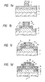
- Figs. 1a to 1d and Figs. 2a to 2d show some steps for use in illustrating different preferred embodiments of the present invention, respectively.
- Figs. 1a to 1d illustrate one example of a manufacturing step for an HBT of the present invention.
- an n-type GaAs layer 2 containing Si of about 5 x 1018 cm-3 doped is accumulated on a semi-insulative GaAs substrate so as to form a collector layer of a thickness of 0.8 ⁇ m.
- a p-type GaAs layer 3 with a thickness of about 100 nm containing Be doped in about 3 x 1019 cm-3 is formed, and an n-type AlGaAs layer 4 with a thickness of about 150 nm containing Si of about 5 x 1017 cm-3 (Al: 30 atom %) is formed as an emitter layer, respectively and lastly an n-type In x Ga 1-x As layer 5 with a thickness of about 200 nm containing doped Si of about 5 x 1018 cm ⁇ 3 (x varies from 0 to 1 toward a surface of it) is formed as a cap layer in sequence and this is grown by a well-known MBE (Molecular Beam Epitaxial growth) process.
- MBE Molecular Beam Epitaxial growth
- WSi is accumulated to show a thickness of about 800 nm by a well-known sputtering process, a non-required part of WSi film is removed by an etching process with a photoresist mask 7 to form an emitter pattern 6.
- Si3N4 may be accumulated.
- an exposed part of the n-type GaAs layer 5 is etched by a reactive ion etching in CCl2F2 gas and inner gas (He) atmosphere with a mask of the emitter pattern 6, and an exposed part of the n-type AlGaAs layer 4 is etched by a chemical etching process, respectively.
- a photoresist mask (not shown) for use in forming the base and the collector regions is provided, then, an exposed part of the p-type GaAs layer is removed by a reactive ion etching using CCl4 as an etching gas so as to form the base region 3. This etching process is further continued and the exposed part of the n-type GaAs layer 2 is slightly etched to form the collector region 2. Then, a well-known CVD is applied to accumulate SiO2 on an entire surface to form the insulation film 8 with a thickness of about 300 nm and after this formation a well-known photoetching is applied to form the contact hole through the SiO2 film 8 for use in connecting the base electrode.
- a reactive ion etching using mixed gas of CHF3 and C2F6 was applied.
- a base electrode 9 composed of AuZn alloy was formed by a well-known vapor deposition and a lift-off technique, and an ohmic contact was got between them through a heat treatment in nitrogen atmosphere (400°C, 2 minutes).
- AuZn alloy film 9' was formed also on the emitter pattern 6.
- the photoresist was coated entirely on the surface in thickness form to flatten the surface, thereafter a dry etching process was carried out on the entire surface at an approximate same etching speed to cause a surface of an AuZn alloy film 9' formed on the emitter pattern 6 to be exposed and the AuZn alloy film 9' was etched by the well-known ion-milling process and removed.
- the collector electrode 10 composed of AuGe alloy was formed by a well-known vapor deposition and the lift-off technique, thereafter the insulation film 11 was formed on an entire surface.
- the insulation film 11, made of spin-on-glass (SOG) is held between the two SiO2 films formed by a CVD process to form a sandwich structure and a total film thickness is about 600 nm.
- a well-known photoetching process is applied to form an opening at a predetermined part of the insulation film 11 through which the surface of the emitter pattern 6 is exposed.
- an insulation film 11, formed on the base electrode 9 and the collector electrode 10 is respectively removed by the photoetching process to form a contact hole, thereafter an electrical conductive film containing Au as major constituent is formed on an entire surface by a well-known vapor depositing process.
- a non-required part of it is removed by a well-known photoetching process using an ion-milling together with a photoresist mask and then wirings are formed. At this time, all the upper surface of the emitter pattern 6 are covered by the wirings 13.
- the emitter pattern 6 is made of electrical conductive material and it is apparent that it may act as an emitter electrode.
- the HBT formed in this embodiment is made such that the emitter electrode 6 is formed equal or larger at least than the emitter region 5.
- an area of a contact portion between the emitter electrode 6 and the wiring 13 is larger than that of the emitter region 5. Due to this fact, it was possible to perform a stable application of a voltage to an emitter-base junction. Further, a thin thickness of the insulation film 8 formed on the sides of the emitter regions 4 and 5 enabled a base parasitic resistance to be reduced.
- a so-called emitter-top type HBT in which the emitter region is placed over the collector and base regions has been described.
- an n-type GaAs layer, an n-type AlGaAs layer acting as an emitter layer, a p-type GaAs layer acting as a base layer and an n-type GaAs layer acting as a collector layer were piled up in this sequence on the substrate and subsequently they were processed substantially in the same manner as above to form the collector-top type HBT and it was recognized to have a substantial similar effect as that of the aforesaid emitter-top type HBT.
- Figs. 2a to 2d illustrate steps for showing another preferred embodiment of the present invention.
- an n-type InGaAs layer (a collector layer) 15 with a thickness of about 300 nm containing Si doped in an n-type dopant of 2 x 1019 cm ⁇ 3, an n-type InGaAs layer 16 with a thickness of about 500 nm containing Si doped in 1 x 1016 cm ⁇ 3
- a p-type InGaAs layer (a base layer) 17 with a thickness of about 50 nm containing Be doped in 1 x 1020cm ⁇ 3
- an n-type InAlAs layer (an emitter layer) 18 with a thickness of 200 nm containing Si doped in 5 x 1017cm ⁇ 3
- an n-type InGaAs layer (a cap layer) 19 with a thickness of 200 nm containing Si doped in 2 x 10
- WSi layer with a film thickness of about 800 nm is formed by applying the well-known sputtering process and the emitter pattern 20 is formed by using a photoetching with a photoresist mask.
- SiO2 film is formed on an entire surface by applying the well-known CVD, the entire surface of SiO2 film is anisotropically etched, SiO2 film formed on a flat surface part is removed and only SiO2 film 21 formed on the side part of the emitter pattern 20 is left.
- a thickness of SiO2 film left on the side part is the same about 400 nm which is a total thickness of an n-type InGaAs layer 19 and an n-type InAlAs layer 18 to be etched in the next step.
- an exposed portion of the n-type InGaAs layer 19 is etched by a reactive ion etching, using and a gas of Cl as etching gas, and another exposed portion of the n-type InAlAs layer 18 is etched by a chemical etching process, respectively, and thereby, the p-type InGaAs layer 17 is exposed.
- the SiO2 layer 21 is removed by the chemical etching.
- the exposed portions of the p-type InGaAs layer 17 and the n-type InGaAs layer 16 are removed by using the well-known photoetching technique with the photoresist mask (not shown) to expose the n-type InGaAs layer 15, and then the photoresist mask is removed.
- SiO2 film 22 with a thickness of about 300 nm is accumulated on an entire surface by the CVD process in the same manner as that of the embodiment 1, thereafter the portions of the SiO2 film 22 where the base, collector and emitter electrodes are provided are etched by the reactive ion etching using mixed gas of CHF3 and C2F6 as the etching gas so as to form holes in SiO2 film 22.
- the SiO2 film 22 formed on the emitter pattern 20 is completely removed and the upper surface of the emitter pattern 20 is exposed, resulting in that as shown in Fig.2c, the emitter pattern 20, the SiO2 film 22' on the sides of the emitters 19 and 18 and the SiO2 film 22 formed on the other portion are left so as to form the contact holes of the emitter, base and collector.
- a stacked film of Mo film and Au film is entirely deposited, thereafter the non-required portion is removed by the well-known lift-off process so as to form the base electrode 23, collector electrode 24 and emitter electrode 25.
- An inter dielectric film 26 having a thickness of 0.6 ⁇ m composed of the SiO2 film made by the CVD process and of the SOG film was entirely formed.
- holes are formed in the inter dielectric film 22 by using the well-known photoetching, and the surfaces of the emitter, base and collector electrodes 25, 23 and 24 are exposed.
- the multi-layer film composed of Mo layer and Au layer is entirely formed by a vapor deposition, non-required portions are removed by the well-known photoethching process using the ion-milling so as to form the wiring 27.
- the upper surface of the emitter electrode 25 is completely exposed and a contact area between the wiring 27 and the emitter electrode 25 is larger than at least an area of the emitter pattern 20.
- the emitter pattern 20 composed of WSi as an emitter electrode and it has an advantage of enabling a quite simplified step to be attained. Due to a thickness of the SiO2 film 21 formed on the side part of the emitter pattern 20 in Fig. 2a, it is possible to reduce an influence caused by the side etching produced in performing an etching of the semiconductor layer and it may provide an advantage of facilitating a fine emitter size.
- the element of the preferred embodiment of the present invention enabled a stable application of the voltage to the emitter-base junction.
- the present invention even if the size of the emitter (or collector) is made quite small, it becomes possible to provide a more stable application of voltage to the emitter-base junction (or the collector-base junction) than that of the prior art HBT and thus this effect can be realized by HBT capable of performing a quite stable operation.
Landscapes
- Bipolar Transistors (AREA)
Applications Claiming Priority (2)
| Application Number | Priority Date | Filing Date | Title |
|---|---|---|---|
| JP30481489A JP3210657B2 (ja) | 1989-11-27 | 1989-11-27 | ヘテロ接合バイポーラトランジスタ |
| JP304814/89 | 1989-11-27 |
Publications (2)
| Publication Number | Publication Date |
|---|---|
| EP0430086A2 true EP0430086A2 (fr) | 1991-06-05 |
| EP0430086A3 EP0430086A3 (en) | 1991-07-03 |
Family
ID=17937572
Family Applications (1)
| Application Number | Title | Priority Date | Filing Date |
|---|---|---|---|
| EP19900122345 Withdrawn EP0430086A3 (en) | 1989-11-27 | 1990-11-22 | Hetero junction bipolar transistor and its manufacturing method |
Country Status (4)
| Country | Link |
|---|---|
| US (1) | US5296733A (fr) |
| EP (1) | EP0430086A3 (fr) |
| JP (1) | JP3210657B2 (fr) |
| KR (1) | KR910010730A (fr) |
Cited By (5)
| Publication number | Priority date | Publication date | Assignee | Title |
|---|---|---|---|---|
| US5296733A (en) * | 1989-11-27 | 1994-03-22 | Hitachi, Ltd. | Hetero junction bipolar transistor with improved electrode wiring contact region |
| US5698871A (en) * | 1994-10-17 | 1997-12-16 | Mitsubishi Denki Kabushiki Kaisha | Heterojunction bipolar transistor |
| EP0881690A1 (fr) * | 1997-05-30 | 1998-12-02 | Thomson-Csf | Transistor bipolaire stabilisé avec éléments isolants électriques |
| US6025615A (en) * | 1992-03-23 | 2000-02-15 | Texas Instruments Incorporated | Microwave heterojunction bipolar transistors with emitters designed for high power applications and method for fabricating same |
| DE10152089A1 (de) * | 2001-10-23 | 2003-05-08 | Infineon Technologies Ag | Verfahren zum Herstellen einer Halbleiter-Struktur |
Families Citing this family (10)
| Publication number | Priority date | Publication date | Assignee | Title |
|---|---|---|---|---|
| JPH06104273A (ja) * | 1992-09-18 | 1994-04-15 | Hitachi Ltd | 半導体装置 |
| JP2913077B2 (ja) * | 1992-09-18 | 1999-06-28 | シャープ株式会社 | 半導体装置 |
| US5734193A (en) * | 1994-01-24 | 1998-03-31 | The United States Of America As Represented By The Secretary Of The Air Force | Termal shunt stabilization of multiple part heterojunction bipolar transistors |
| US5773334A (en) * | 1994-09-26 | 1998-06-30 | Toyota Jidosha Kabushiki Kaisha | Method of manufacturing a semiconductor device |
| DE19842106A1 (de) * | 1998-09-08 | 2000-03-09 | Inst Halbleiterphysik Gmbh | Vertikaler Bipolartransistor und Verfahren zu seiner Herstellung |
| US6437419B1 (en) * | 1999-11-29 | 2002-08-20 | Fairchild Semiconductor Corporation | Emitter ballast resistor with enhanced body effect to improve the short circuit withstand capability of power devices |
| US7598148B1 (en) | 2004-10-15 | 2009-10-06 | Fields Charles H | Non-self-aligned heterojunction bipolar transistor and a method for preparing a non-self-aligned heterojunction bipolar transistor |
| US7875523B1 (en) | 2004-10-15 | 2011-01-25 | Hrl Laboratories, Llc | HBT with emitter electrode having planar side walls |
| US7396731B1 (en) | 2004-10-15 | 2008-07-08 | Hrl Laboratories, Llc | Method for preparing a non-self-aligned heterojunction bipolar transistor with a small emitter-to-base spacing |
| JPWO2021214866A1 (fr) * | 2020-04-21 | 2021-10-28 |
Family Cites Families (11)
| Publication number | Priority date | Publication date | Assignee | Title |
|---|---|---|---|---|
| EP0228712B1 (fr) * | 1986-01-06 | 1995-08-09 | Sel Semiconductor Energy Laboratory Co., Ltd. | Dispositif de conversion photo-électrique à haute vitesse de réponse et méthode pour sa fabrication |
| JPH0713968B2 (ja) * | 1986-01-07 | 1995-02-15 | 富士通株式会社 | 化合物半導体装置の製造方法 |
| EP0240307B1 (fr) * | 1986-04-01 | 1993-12-22 | Matsushita Electric Industrial Co., Ltd. | Transistor bipolaire et son procédé de fabrication |
| JPS634677A (ja) * | 1986-06-24 | 1988-01-09 | Nec Corp | 半導体装置の製造方法 |
| JP2590842B2 (ja) * | 1986-10-29 | 1997-03-12 | ソニー株式会社 | ヘテロ接合型バイポーラトランジスタ |
| US4962053A (en) * | 1987-01-30 | 1990-10-09 | Texas Instruments Incorporated | Bipolar transistor fabrication utilizing CMOS techniques |
| US4958208A (en) * | 1987-08-12 | 1990-09-18 | Nec Corporation | Bipolar transistor with abrupt potential discontinuity in collector region |
| JPS6477167A (en) * | 1987-09-18 | 1989-03-23 | Nippon Telegraph & Telephone | Hetero-bipolar transistor |
| US5064772A (en) * | 1988-08-31 | 1991-11-12 | International Business Machines Corporation | Bipolar transistor integrated circuit technology |
| EP0387010A3 (fr) * | 1989-03-08 | 1990-10-10 | Matsushita Electric Industrial Co., Ltd. | Transistor bipolaire à hétérojonction |
| JP3210657B2 (ja) * | 1989-11-27 | 2001-09-17 | 株式会社日立製作所 | ヘテロ接合バイポーラトランジスタ |
-
1989
- 1989-11-27 JP JP30481489A patent/JP3210657B2/ja not_active Expired - Fee Related
-
1990
- 1990-11-19 US US07/615,381 patent/US5296733A/en not_active Expired - Fee Related
- 1990-11-22 EP EP19900122345 patent/EP0430086A3/en not_active Withdrawn
- 1990-11-26 KR KR1019900019166A patent/KR910010730A/ko not_active Withdrawn
Cited By (8)
| Publication number | Priority date | Publication date | Assignee | Title |
|---|---|---|---|---|
| US5296733A (en) * | 1989-11-27 | 1994-03-22 | Hitachi, Ltd. | Hetero junction bipolar transistor with improved electrode wiring contact region |
| US6025615A (en) * | 1992-03-23 | 2000-02-15 | Texas Instruments Incorporated | Microwave heterojunction bipolar transistors with emitters designed for high power applications and method for fabricating same |
| US5698871A (en) * | 1994-10-17 | 1997-12-16 | Mitsubishi Denki Kabushiki Kaisha | Heterojunction bipolar transistor |
| EP0881690A1 (fr) * | 1997-05-30 | 1998-12-02 | Thomson-Csf | Transistor bipolaire stabilisé avec éléments isolants électriques |
| FR2764118A1 (fr) * | 1997-05-30 | 1998-12-04 | Thomson Csf | Transistor bipolaire stabilise avec elements isolants electriques |
| US6031255A (en) * | 1997-05-30 | 2000-02-29 | Thomson-Csf | Bipolar transistor stabilized with electrical insulating elements |
| US6451659B1 (en) | 1997-05-30 | 2002-09-17 | Thomson-Csf | Method for forming a bipolar transistor stabilized with electrical insulating elements |
| DE10152089A1 (de) * | 2001-10-23 | 2003-05-08 | Infineon Technologies Ag | Verfahren zum Herstellen einer Halbleiter-Struktur |
Also Published As
| Publication number | Publication date |
|---|---|
| KR910010730A (ko) | 1991-06-29 |
| JP3210657B2 (ja) | 2001-09-17 |
| EP0430086A3 (en) | 1991-07-03 |
| US5296733A (en) | 1994-03-22 |
| JPH03166734A (ja) | 1991-07-18 |
Similar Documents
| Publication | Publication Date | Title |
|---|---|---|
| US5729033A (en) | Fully self-aligned submicron heterojunction bipolar transistor | |
| US4683487A (en) | Heterojunction bipolar transistor | |
| US5296733A (en) | Hetero junction bipolar transistor with improved electrode wiring contact region | |
| US6462362B1 (en) | Heterojunction bipolar transistor having prevention layer between base and emitter | |
| EP0177246B1 (fr) | Transistor bipolaire à hétérojonction et procédé de fabrication | |
| US6885042B2 (en) | Hetero-junction bipolar transistor and a manufacturing method of the same | |
| US5242843A (en) | Method for making a heterojunction bipolar transistor with improved high frequency response | |
| JP4288852B2 (ja) | バイポーラトランジスタの製造方法 | |
| US6873029B2 (en) | Self-aligned bipolar transistor | |
| EP0335720B1 (fr) | Transistor bipolaire et procédé pour sa fabrication | |
| US6828603B2 (en) | Hetero-bipolar transistor with a sub-collector layer having a first portion and plural second portions | |
| JPH05136159A (ja) | ヘテロ接合型バイポーラトランジスタ及びその製造方法 | |
| JP3349267B2 (ja) | ヘテロバイポーラ型半導体装置とその製造方法 | |
| US5471078A (en) | Self-aligned heterojunction bipolar transistor | |
| EP1471580A2 (fr) | Transistor bipolaire et procédé pour sa fabrication | |
| JP4026347B2 (ja) | 化合物半導体バイポーラトランジスタの製造方法 | |
| US5153692A (en) | Semiconductor device | |
| JP3135003B2 (ja) | ヘテロ接合バイポーラトランジスタの製造方法 | |
| JP4092597B2 (ja) | 半導体装置及びその製造方法 | |
| JPH098055A (ja) | ヘテロバイポーラ型半導体装置及びその製造方法 | |
| KR100197001B1 (ko) | 바이폴라소자 및 그 제조방법 | |
| JP3210354B2 (ja) | ヘテロ接合バイポーラトランジスタの製造方法 | |
| JP2005159112A (ja) | 半導体装置および半導体装置の製造方法 | |
| WO1998034274A1 (fr) | Procede a auto-alignement pour la fabrication d'une corniche de passivation dans un transistor bipolaire a heterojonction | |
| JPH07283231A (ja) | 半導体装置とその製造方法 |
Legal Events
| Date | Code | Title | Description |
|---|---|---|---|
| PUAI | Public reference made under article 153(3) epc to a published international application that has entered the european phase |
Free format text: ORIGINAL CODE: 0009012 |
|
| PUAL | Search report despatched |
Free format text: ORIGINAL CODE: 0009013 |
|
| 17P | Request for examination filed |
Effective date: 19901212 |
|
| AK | Designated contracting states |
Kind code of ref document: A2 Designated state(s): DE FR GB |
|
| AK | Designated contracting states |
Kind code of ref document: A3 Designated state(s): DE FR GB |
|
| 17Q | First examination report despatched |
Effective date: 19931025 |
|
| STAA | Information on the status of an ep patent application or granted ep patent |
Free format text: STATUS: THE APPLICATION IS DEEMED TO BE WITHDRAWN |
|
| 18D | Application deemed to be withdrawn |
Effective date: 19950915 |