EP0433141A1 - Redundanzschaltung für Speicher - Google Patents
Redundanzschaltung für Speicher Download PDFInfo
- Publication number
- EP0433141A1 EP0433141A1 EP90403478A EP90403478A EP0433141A1 EP 0433141 A1 EP0433141 A1 EP 0433141A1 EP 90403478 A EP90403478 A EP 90403478A EP 90403478 A EP90403478 A EP 90403478A EP 0433141 A1 EP0433141 A1 EP 0433141A1
- Authority
- EP
- European Patent Office
- Prior art keywords
- group
- column
- memory
- columns
- redundancy
- Prior art date
- Legal status (The legal status is an assumption and is not a legal conclusion. Google has not performed a legal analysis and makes no representation as to the accuracy of the status listed.)
- Granted
Links
- 230000015654 memory Effects 0.000 title claims abstract description 98
- 230000002950 deficient Effects 0.000 claims abstract description 42
- 230000006870 function Effects 0.000 claims description 8
- 230000003213 activating effect Effects 0.000 claims description 4
- 230000002401 inhibitory effect Effects 0.000 claims description 2
- 230000005540 biological transmission Effects 0.000 claims 1
- 230000008439 repair process Effects 0.000 description 7
- 230000004913 activation Effects 0.000 description 4
- 238000004519 manufacturing process Methods 0.000 description 3
- 230000008520 organization Effects 0.000 description 3
- 238000001514 detection method Methods 0.000 description 2
- 230000010354 integration Effects 0.000 description 2
- 230000008859 change Effects 0.000 description 1
- 239000004020 conductor Substances 0.000 description 1
- 230000007547 defect Effects 0.000 description 1
- 238000010586 diagram Methods 0.000 description 1
- 230000006872 improvement Effects 0.000 description 1
- 239000011159 matrix material Substances 0.000 description 1
- 230000002093 peripheral effect Effects 0.000 description 1
Images

Classifications
-
- G—PHYSICS
- G11—INFORMATION STORAGE
- G11C—STATIC STORES
- G11C29/00—Checking stores for correct operation ; Subsequent repair; Testing stores during standby or offline operation
- G11C29/70—Masking faults in memories by using spares or by reconfiguring
- G11C29/78—Masking faults in memories by using spares or by reconfiguring using programmable devices
- G11C29/80—Masking faults in memories by using spares or by reconfiguring using programmable devices with improved layout
-
- G—PHYSICS
- G11—INFORMATION STORAGE
- G11C—STATIC STORES
- G11C29/00—Checking stores for correct operation ; Subsequent repair; Testing stores during standby or offline operation
- G11C29/70—Masking faults in memories by using spares or by reconfiguring
- G11C29/78—Masking faults in memories by using spares or by reconfiguring using programmable devices
- G11C29/84—Masking faults in memories by using spares or by reconfiguring using programmable devices with improved access time or stability
- G11C29/846—Masking faults in memories by using spares or by reconfiguring using programmable devices with improved access time or stability by choosing redundant lines at an output stage
Definitions
- the invention relates to memories made in integrated circuit and, more particularly, in a memory which includes redundant columns, a circuit for activating redundant columns.
- memories which include redundancy systems, that is to say which include more memory cells than is necessary and connection circuits in order to be able to use the additional cells (“ redundant cells ”) instead of normal cells that prove to be defective.
- redundant cells the additional cells
- the defective cells are detected, electrical connection paths are established making it possible to disconnect the defective cells and to connect redundant cells instead, so that the memory appears generally good to the user despite the presence of defective elements.
- the memories are organized in principle in rows and columns of cells; we read the information on a column conductor (sometimes called "bit line") contained in a cell located at the crossroads of this column and of a determined row defined by a row address.
- a column conductor sometimes called "bit line”
- Redundancy systems do not generally replace a faulty cell with a redundant cell. They more often replace a row or column with one or more faults by a redundant row or column.
- the number of columns is much greater than z. For example we have 512 columns even if we want to supply 8 or 16 or 32 bit words at the memory output.
- the columns are arranged in z sets of columns, each set corresponding to a data output pad from the memory; on each plot, each data item is collected from a determined column of a set corresponding to this plot and not to another.
- each plot corresponds to an amplifier for reading stored data.
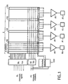
- FIG. 1 very schematically represents a memory of this type: the memory is organized in words of z bits; there are z output pads (P0 to P3), z read amplifiers (A0 to A3), z sets of columns each corresponding to an amplifier and a respective pad. Each set has p columns of cells. Finally, each column has n cells, that is to say that the memory has n rows of cells.
- a line decoder DL intended to receive a line address AL and to select a row among n as a function of this address.
- a column decoder intended to receive a column address AC and to select a column from p as a function of this address.
- the selection of a column address does not designate a single column but a column in each of the z sets and connects this column to the sense amplifier and therefore to the corresponding output pad.
- the application of a row address and a column address therefore establishes a z-bit word from z columns on the outputs. These z columns are distributed in the z sets; they all occupy the same rank (among p possible ranks) in the different sets.
- the column address actually designates a determined rank among p, for all the sets simultaneously.
- the memory can include redundant rows (not shown since we are only interested in this invention in column redundancy) and redundant columns; for example, a group of redundant columns is provided for each of the z sets.
- the groups of redundant columns are controlled by a redundancy activation circuit CAR. This circuit receives the column addresses AC, checks whether they correspond to a defective column address, and, if so, deactivates the column decoder DC and selects a redundancy column to replace it.
- the selection circuit is arranged for the selection circuit to designate a redundancy column simultaneously in each of the groups CR0 to CR3 (just as the column decoder DC simultaneously selects a column of each set). But that means that when a column is defective, in a determined set, we replace not only this column but all the columns having the same column address and being part of the other sets.
- redundancy is similar but is complicated in memories organized differently, and in particular memories which, because of their high storage capacity and their integration density, include several read amplifiers (2 or 4 or even more) by data pad. An address bit (or 2 or more) is reserved for the selection of the sense amplifier.
- the set of columns associated with each pad is now divided into several groups each corresponding to a respective amplifier.
- FIG. 2 Such a memory is shown in FIG. 2.
- the organization of the rows and the line decoder are not shown, since only the arrangement of the columns concerns the redundancy of columns.
- the groups are designated by G0a and G0b for the first set E0, and by G1a and G1b for the second set E1, etc.
- the amplifiers are designated by A0a and A0b for the first set E0, and by A1a and A1b for the second, etc.
- Each group has p columns.
- the application of a word to the z memory outputs is done by selecting a row address AL, a column address AC, and a post-selection address AP.
- the line address AL designates a row of cells;
- the column address AC designates one column among p in each group, that is to say in total k times z columns, all the columns having the same rank among p rows in their respective set;
- the post selection address AP defines an amplifier rank among k in each set, or, which amounts to the same thing, a group rank of columns among k group ranks in a set; this results in the selection of an amplifier among k in each set, that is to say z amplifiers in total all having the same rank among k ranks.
- a word of z bits from columns having all the same rank (defined by AC) in the groups to which they belong will be transmitted to the data pads.
- the groups all having the same rank (defined by AP) in the sets to which they belong.
- a respective group of redundancy columns CR0a, CR0b to CR3a, CR3b is provided.
- Each group of redundancy columns comprises r columns, which means that with a group it is possible to repair a priori r defective columns.
- the architecture does not allow, as we will see, to repair a total number of columns of z times k times r (z.k.r), although there are 2 times k times r columns of redundancy.
- FIG. 2 indicates the overall constitution of the redundancy column selection circuit: it includes a comparator (COMP) receiving the address of column AC and comparing this address with addresses stored in a register for storing addresses of defective columns ( RS). If there is a coincidence, the comparator deactivates the DC column decoder to prevent it from selecting the defective column and activates a redundant column selection circuit CSR. The latter selects, according to the result of the comparison, one of the r redundancy columns of each set, simultaneously for all sets. All the redundancy columns of the same rank (among r possible rows) of the various groups CR0a, CR0b to CR3a, CR3b are therefore selected.
- COMP comparator
- the address storage register RS comprises a maximum of r memories, each making it possible to store the address of a column among p.
- the address actually stored is the AC column address of a defective column, regardless of the group to which it belongs. All the columns having the same address of column AC are replaced by redundancy columns having the same rank among r. There are z.k replacements for a defective column.
- the second is to ensure that the redundancy selection circuit is able to select any redundancy column indifferently and to route it to any amplifier, without necessarily selecting a column simultaneously in all the groups.
- this solution uses a lot of routing circuits, precisely at places close to the column outlets where there is not much room.
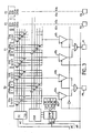
- FIG. 3 a third possible solution is shown in FIG. 3. It consists in using a selection circuit CSR which separately controls the redundancy columns of the k different groups.
- the selection circuit will designate one column among kr in each set and not one column among r in each group; only the redundancy columns which are in groups of the same rank will be selected; to illustrate this, we can say for example that the second redundant column is selected from the groups of redundant columns CR0a, CR1a, CR2a, CR3a, but without selecting the second redundant column from the other groups CR0b to CR3b.
- all the second columns of all the groups CR0a, CR0b to CR3a, CR3b were necessarily selected.
- the object of the present invention is to propose a redundancy activation circuit which allows an increase in the possibilities of repairing a memory of the type of FIG. 2 having several amplifiers per data pad.
- the improvement is of the same order as that obtained in FIG. 3 compared with FIG. 2, but it minimizes the problems of congestion by rejecting to added sparse peripheral zones the connections added in order to increase the possibilities of repair. .
- a storage register for defective addresses which comprises k groups of r zones of memory allowing each to contain a column address.
- Each group of zones corresponds to one rank of amplifier among k.
- Each group of r memory areas will be dedicated to repairing the columns of the group corresponding to an amplifier of given rank and will not be able to repair the columns corresponding to the other amplifiers and to the other column groups not having the same rank.
- the post selection address AP used to designate the rank of the amplifiers to be used and effectively used to activate all the amplifiers of this rank will also be used to designate the group of faulty address memories and to activate only the group of the row corresponding to that of the activated amplifiers.
- the selection circuit CSR remains the same as in FIG. 2 and acts in the same way on the redundant columns, but the comparator is likely to be connected to k times r memory areas (and not r areas as in FIG. 2), and the post selection address received by the memory designates a group from the k groups of memory zones so that this group is effectively connected to the comparator.
- r defective columns can be independently repaired located in groups of the same rank among k, and this for each of the rows.
- the comparator is permanently connected to k times r memory areas and must provide the selection circuit not only with one rank among r but also with one rank among k.
- the memory zones in the case of FIG. 3 must store both the column address AC and the post-selection address AF, and the comparator must provide a comparison on these two address portions.
- the comparator is only connected at a given time to r zones and not k times r, it designates a rank among r, and finally it makes comparisons only on the addresses of column AC.
- the circuit according to the invention makes it possible to reject at the periphery of the memory (where the faulty address storage registers are) the additional connections required by the increase in repair possibilities. It does not require placing switches where there would be no room, that is to say between the outputs of the columns and the amplifiers.
- a circuit for activating a redundancy column in an integrated memory with redundancy of data columns comprising:
- a network of memory elements organized in n rows and z sets of k groups of p columns, with n, z, k and p different from the unit, each set corresponding to a respective data pad among z, and each group corresponding to a respective reading amplifier among k amplifiers connected to this block, so that data from a column of a determined group in a determined set is applied to the block corresponding to this set by the amplifier corresponding to this group,
- the redundant column activation circuit being characterized in that it comprises
- a redundancy column selection circuit for selecting a redundancy column among r simultaneously in all the groups of all the sets, that is to say for simultaneously selecting zk redundancy columns of the same rank (1 among r) belonging all to different groups and sets,
- each group of memories comprising in memory r column addresses and each address making it possible to designate a column among p, each group of memories being dedicated to storing addresses of defective columns corresponding to a single row of column group among k, without distinction between the sets to which the defective columns can belong (that is to say that the first group of memories corresponds to a defective column address which belongs to the first group of any of the sets, the second group of memories corresponds to a column address belonging to the second group of columns of any set, etc.),
- a memory group selection means capable of selecting a group of memories among k during the reception by memory of a group address among k
- FIG. 4 shows a block diagram of a redundancy system according to the invention.
- each group corresponds to an amplifier, and the different amplifiers corresponding to the same set are connected to the same data output pad. There are therefore z output pads (P0 to P3 in the figure).
- the amplifiers of the first set are A0a and A0b corresponding to the groups G0a and G0b respectively, A1a and A1b corresponding to groups G1a and G1b, etc.
- the row of the column among p possible rows within a group is defined by a column address AC.
- the rank of the group or amplifier among k possible ranks within a set is defined by a post selection address AP.
- the column address selects all columns of the same rank from all groups. It makes this selection using a multiplexer placed at the outlet of the columns.
- the post selection address selects all groups of the same rank in all the sets simultaneously. This post selection is carried out by activating all the amplifiers of the same rank (1 among k) of the different sets. The activation of an amplifier connects the columns of the group corresponding to this amplifier (and more exactly the column selected in this group by the address AC) to the block of the assembly in which the group is located, block to which the 'amplifier.
- the redundancy columns can be selected using a redundancy circuit which essentially comprises a comparator COMP capable of comparing the column address AC received by the memory with addresses of defective columns stored in a storage register RS. When a defective address is applied to the memory, it is recognized by the comparator, the function of which is then to inhibit the DC column decoder and to select a redundancy column to replace the defective column.
- a redundancy circuit which essentially comprises a comparator COMP capable of comparing the column address AC received by the memory with addresses of defective columns stored in a storage register RS.
- the groups of redundancy columns are each associated with an amplifier and are connected to this amplifier via a multiplexer in the same way as the columns of memory cells. From the main network are connected to the amplifiers via a multiplexer. But while the connection of the columns of the main network is controlled by the DC decoder, the connection of the redundant columns is controlled by a selection circuit of redundant columns CSR coupled to the output of the comparator.
- the storage register comprises k groups of r memory areas, each area being able to store a column address defining a defective column (among p).
- the group in which this column is located is not identified or stored in the memory area of the storage register.
- each group of r memory areas of determined rank is intended for exclusively store a faulty column address located in a group of columns of this same rank.
- the second group includes two other areas M1b and M2b for storing defective addresses of columns located in the second rank groups G0b to G3b only.
- the register is controlled by the post selection address AP, which precisely defines rank 1 among k groups and amplifiers, and which will be used according to the invention also defines rank 1 among k of the group of storage memories of the register RS.
- the register RS Under the control of a bus PS transmitting the post selection address AP, the register RS provides the comparator COMP only with the contents of the memory areas of the group whose rank corresponds to this address. In this group there are ar memory areas, that is to say r possibilities for storing addresses of defective columns. If one precisely corresponds to the AP address received at the memory input, the comparator signals it and indicates to the selection circuit CSR which is the memory from which the detection was made.
- the selection circuit CSR is then capable, under the command of the comparator, of defining a redundancy column among r, simultaneously for all the groups of r columns of all the sets it does not make the difference between a group and another or a together and another, which minimizes the size of the multiplexer it controls (same size as in Figure 2).
- the designated redundancy column (among r) is that which corresponds to the memory (among r) which contained the defective address recognized by the comparator.
- a column from among r redundancy columns is therefore selected from each of the groups regardless of their rank among k, and it is connected to the input of the amplifier corresponding to this group. But only the activated amplifiers will effectively transmit the information to a pad. And only the amplifiers of a determined rank among k are activated, as a function of the post selection address AP. However, the detection of faulty addresses was only authorized for the columns corresponding to the same rank among k.
- the object of the invention has thus been achieved, which is to increase the possibilities of redundancy without increasing the bulk in the immediate vicinity of the columns of the memory; in particular, the size of the multiplexer which, under the control of the circuit CSR, designates one column among r, is minimized, and the added additional elements, such as the additional memory areas of the register, have been rejected towards the periphery.
- these memory zones can be constituted by batteries of fuses, or by electrically programmable memory cells such as EPROM or EEPROM cells.
Landscapes
- For Increasing The Reliability Of Semiconductor Memories (AREA)
- Techniques For Improving Reliability Of Storages (AREA)
Applications Claiming Priority (2)
| Application Number | Priority Date | Filing Date | Title |
|---|---|---|---|
| FR8916338 | 1989-12-11 | ||
| FR8916338A FR2655763B1 (fr) | 1989-12-11 | 1989-12-11 | Circuit de redondance pour memoire. |
Publications (2)
| Publication Number | Publication Date |
|---|---|
| EP0433141A1 true EP0433141A1 (de) | 1991-06-19 |
| EP0433141B1 EP0433141B1 (de) | 1992-07-01 |
Family
ID=9388355
Family Applications (1)
| Application Number | Title | Priority Date | Filing Date |
|---|---|---|---|
| EP90403478A Expired - Lifetime EP0433141B1 (de) | 1989-12-11 | 1990-12-06 | Redundanzschaltung für Speicher |
Country Status (4)
| Country | Link |
|---|---|
| US (1) | US5504712A (de) |
| EP (1) | EP0433141B1 (de) |
| DE (1) | DE69000175T2 (de) |
| FR (1) | FR2655763B1 (de) |
Cited By (1)
| Publication number | Priority date | Publication date | Assignee | Title |
|---|---|---|---|---|
| EP0940753A3 (de) * | 1998-03-04 | 1999-09-22 | Nec Corporation | Halbleiterspeicherschaltung mit Redundanz |
Families Citing this family (5)
| Publication number | Priority date | Publication date | Assignee | Title |
|---|---|---|---|---|
| JPH09147595A (ja) * | 1995-11-24 | 1997-06-06 | Nec Corp | 半導体記憶装置 |
| KR100224774B1 (ko) * | 1996-06-29 | 1999-10-15 | 김영환 | 반도체 메모리 장치의 컬럼 리던던시 회로 |
| KR20020043796A (ko) * | 2000-12-04 | 2002-06-12 | 박종섭 | 반도체 메모리 소자의 구제 회로 |
| US20020108073A1 (en) * | 2001-02-02 | 2002-08-08 | Hughes Brian William | System for and method of operating a programmable column fail counter for redundancy allocation |
| EP1646052A1 (de) * | 2004-10-07 | 2006-04-12 | Infineon Technologies AG | Speicherschaltung mit flexibler bitleitungs- und oder wortleitungsbezogener Ersetzung von defekten Speicherzellen |
Citations (3)
| Publication number | Priority date | Publication date | Assignee | Title |
|---|---|---|---|---|
| EP0104120A2 (de) * | 1982-09-20 | 1984-03-28 | Fairchild Semiconductor Corporation | Redundante Spalten für bytebreite Speicher |
| US4601019A (en) * | 1983-08-31 | 1986-07-15 | Texas Instruments Incorporated | Memory with redundancy |
| FR2611301A1 (fr) * | 1987-02-24 | 1988-08-26 | Thomson Semiconducteurs | Memoire integree avec redondance de colonnes de donnees |
Family Cites Families (3)
| Publication number | Priority date | Publication date | Assignee | Title |
|---|---|---|---|---|
| JPH01119995A (ja) * | 1987-11-02 | 1989-05-12 | Toshiba Corp | 半導体メモリ |
| FR2636464B1 (fr) * | 1988-09-14 | 1990-10-26 | Sgs Thomson Microelectronics | Memoire eprom avec signature interne concernant notamment le mode de programmation |
| JP2664236B2 (ja) * | 1989-02-01 | 1997-10-15 | 富士通株式会社 | 半導体記憶装置 |
-
1989
- 1989-12-11 FR FR8916338A patent/FR2655763B1/fr not_active Expired - Lifetime
-
1990
- 1990-12-06 DE DE9090403478T patent/DE69000175T2/de not_active Expired - Fee Related
- 1990-12-06 EP EP90403478A patent/EP0433141B1/de not_active Expired - Lifetime
-
1993
- 1993-07-23 US US08/097,598 patent/US5504712A/en not_active Expired - Lifetime
Patent Citations (4)
| Publication number | Priority date | Publication date | Assignee | Title |
|---|---|---|---|---|
| EP0104120A2 (de) * | 1982-09-20 | 1984-03-28 | Fairchild Semiconductor Corporation | Redundante Spalten für bytebreite Speicher |
| US4601019A (en) * | 1983-08-31 | 1986-07-15 | Texas Instruments Incorporated | Memory with redundancy |
| US4601019B1 (en) * | 1983-08-31 | 1997-09-30 | Texas Instruments Inc | Memory with redundancy |
| FR2611301A1 (fr) * | 1987-02-24 | 1988-08-26 | Thomson Semiconducteurs | Memoire integree avec redondance de colonnes de donnees |
Non-Patent Citations (1)
| Title |
|---|
| IEEE JOURNAL OF SOLID-STATE CIRCUITS, vol. 24, no. 1, février 1989, pages 43-49, IEEE, New York, US; Y. NISHIMURA et al.: "A redundancy test-time reduction technique in 1-Mbit DRAM with a multibit test mode" * |
Cited By (2)
| Publication number | Priority date | Publication date | Assignee | Title |
|---|---|---|---|---|
| EP0940753A3 (de) * | 1998-03-04 | 1999-09-22 | Nec Corporation | Halbleiterspeicherschaltung mit Redundanz |
| US6041006A (en) * | 1998-03-04 | 2000-03-21 | Nec Corporation | Semiconductor memory device |
Also Published As
| Publication number | Publication date |
|---|---|
| FR2655763B1 (fr) | 1992-01-17 |
| US5504712A (en) | 1996-04-02 |
| EP0433141B1 (de) | 1992-07-01 |
| DE69000175D1 (de) | 1992-08-06 |
| FR2655763A1 (fr) | 1991-06-14 |
| DE69000175T2 (de) | 1993-02-25 |
Similar Documents
| Publication | Publication Date | Title |
|---|---|---|
| EP0666573B1 (de) | Source programmierter nichtflüchtiger Flip-Flop für Speicherredundanzschaltung | |
| JP3865789B2 (ja) | インタリーブされた入力回路を備えるプログラマブル論理装置のための冗長回路 | |
| FR2688328A1 (fr) | Circuit a redondance de rangees pour dispositif a memoire a semi-conducteurs pour reparer ou remplacer une cellule defectueuse d'un reseau de cellules a memoire. | |
| EP0234907B1 (de) | Halbleiterspeichergerät mit redundanter Speicherzelle | |
| EP0626760B1 (de) | Als Zellenmatrix-Netzwerk organisiertes elektronisches System | |
| FR2787233A1 (fr) | Procede pour verifier l'integrite des circuits de decodage d'une memoire | |
| US6094385A (en) | Repairable memory cell for a memory cell array | |
| JPH07153296A (ja) | 半導体記憶装置 | |
| FR2772507A1 (fr) | Dispositif de memoire a circuits integres ayant des lignes d'entree et de sortie de donnees s'etendant dans la direction des colonnes, et circuits et procedes pour reparer des cellules defectueuses | |
| EP0433141B1 (de) | Redundanzschaltung für Speicher | |
| FR2611301A1 (fr) | Memoire integree avec redondance de colonnes de donnees | |
| FR2736175A1 (fr) | Circuit de reparation de cellules de memoire en panne dans une memoire a semi-conducteurs | |
| FR2576133A1 (fr) | Memoire en circuit integre a haute fiabilite | |
| US6327197B1 (en) | Structure and method of a column redundancy memory | |
| EP0977120B1 (de) | Fehlerkorrektur in einem ROM mittels Redundanz | |
| FR2665793A1 (fr) | Circuit integre de memoire avec redondance et adressage ameliore en mode de test. | |
| EP0432004B1 (de) | Redundanzschaltung mit Speicherung der Position des Ausgangs | |
| WO1994006082A1 (fr) | Circuit de memoire avec redondance | |
| FR2680590A1 (fr) | Agencement d'un reseau de cellules redondant pour un dispositif de memoire a semiconducteurs. | |
| FR2679692A1 (fr) | Redondance de memoire a semiconducteurs. | |
| US5896329A (en) | Repairable memory cell for a memory cell array | |
| FR2644924A1 (fr) | Circuit de selection d'une colonne redondante dans une memoire integree avec redondance de colonnes de donnees | |
| JP2558787B2 (ja) | 記憶装置 | |
| JP3352487B2 (ja) | 冗長メモリセルを備えたメモリ | |
| FR2764095A1 (fr) | Circuit de memoire avec redondance dynamique |
Legal Events
| Date | Code | Title | Description |
|---|---|---|---|
| PUAI | Public reference made under article 153(3) epc to a published international application that has entered the european phase |
Free format text: ORIGINAL CODE: 0009012 |
|
| AK | Designated contracting states |
Kind code of ref document: A1 Designated state(s): DE FR GB IT |
|
| 17P | Request for examination filed |
Effective date: 19910502 |
|
| 17Q | First examination report despatched |
Effective date: 19911028 |
|
| GRAA | (expected) grant |
Free format text: ORIGINAL CODE: 0009210 |
|
| ITF | It: translation for a ep patent filed | ||
| AK | Designated contracting states |
Kind code of ref document: B1 Designated state(s): DE FR GB IT |
|
| REF | Corresponds to: |
Ref document number: 69000175 Country of ref document: DE Date of ref document: 19920806 |
|
| GBT | Gb: translation of ep patent filed (gb section 77(6)(a)/1977) | ||
| PLBE | No opposition filed within time limit |
Free format text: ORIGINAL CODE: 0009261 |
|
| STAA | Information on the status of an ep patent application or granted ep patent |
Free format text: STATUS: NO OPPOSITION FILED WITHIN TIME LIMIT |
|
| 26N | No opposition filed | ||
| REG | Reference to a national code |
Ref country code: FR Ref legal event code: D6 |
|
| PGFP | Annual fee paid to national office [announced via postgrant information from national office to epo] |
Ref country code: DE Payment date: 20001129 Year of fee payment: 11 |
|
| REG | Reference to a national code |
Ref country code: GB Ref legal event code: IF02 |
|
| PG25 | Lapsed in a contracting state [announced via postgrant information from national office to epo] |
Ref country code: DE Free format text: LAPSE BECAUSE OF NON-PAYMENT OF DUE FEES Effective date: 20020702 |
|
| PGFP | Annual fee paid to national office [announced via postgrant information from national office to epo] |
Ref country code: GB Payment date: 20021204 Year of fee payment: 13 |
|
| PGFP | Annual fee paid to national office [announced via postgrant information from national office to epo] |
Ref country code: FR Payment date: 20021210 Year of fee payment: 13 |
|
| PG25 | Lapsed in a contracting state [announced via postgrant information from national office to epo] |
Ref country code: GB Free format text: LAPSE BECAUSE OF NON-PAYMENT OF DUE FEES Effective date: 20031206 |
|
| GBPC | Gb: european patent ceased through non-payment of renewal fee |
Effective date: 20031206 |
|
| PG25 | Lapsed in a contracting state [announced via postgrant information from national office to epo] |
Ref country code: FR Free format text: LAPSE BECAUSE OF NON-PAYMENT OF DUE FEES Effective date: 20040831 |
|
| REG | Reference to a national code |
Ref country code: FR Ref legal event code: ST |
|
| PG25 | Lapsed in a contracting state [announced via postgrant information from national office to epo] |
Ref country code: IT Free format text: LAPSE BECAUSE OF NON-PAYMENT OF DUE FEES;WARNING: LAPSES OF ITALIAN PATENTS WITH EFFECTIVE DATE BEFORE 2007 MAY HAVE OCCURRED AT ANY TIME BEFORE 2007. THE CORRECT EFFECTIVE DATE MAY BE DIFFERENT FROM THE ONE RECORDED. Effective date: 20051206 |