EP0433174A1 - Integrierte Schaltung mit vollständigem Schutz gegen Ultraviolettstrahlen - Google Patents
Integrierte Schaltung mit vollständigem Schutz gegen Ultraviolettstrahlen Download PDFInfo
- Publication number
- EP0433174A1 EP0433174A1 EP90403570A EP90403570A EP0433174A1 EP 0433174 A1 EP0433174 A1 EP 0433174A1 EP 90403570 A EP90403570 A EP 90403570A EP 90403570 A EP90403570 A EP 90403570A EP 0433174 A1 EP0433174 A1 EP 0433174A1
- Authority
- EP
- European Patent Office
- Prior art keywords
- metal
- cell
- diffusion
- ring
- substrate
- Prior art date
- Legal status (The legal status is an assumption and is not a legal conclusion. Google has not performed a legal analysis and makes no representation as to the accuracy of the status listed.)
- Granted
Links
Images


Classifications
-
- H—ELECTRICITY
- H10—SEMICONDUCTOR DEVICES; ELECTRIC SOLID-STATE DEVICES NOT OTHERWISE PROVIDED FOR
- H10D—INORGANIC ELECTRIC SEMICONDUCTOR DEVICES
- H10D64/00—Electrodes of devices having potential barriers
- H10D64/60—Electrodes characterised by their materials
- H10D64/66—Electrodes having a conductor capacitively coupled to a semiconductor by an insulator, e.g. MIS electrodes
- H10D64/661—Electrodes having a conductor capacitively coupled to a semiconductor by an insulator, e.g. MIS electrodes the conductor comprising a layer of silicon contacting the insulator, e.g. polysilicon having vertical doping variation
-
- H—ELECTRICITY
- H10—SEMICONDUCTOR DEVICES; ELECTRIC SOLID-STATE DEVICES NOT OTHERWISE PROVIDED FOR
- H10B—ELECTRONIC MEMORY DEVICES
- H10B69/00—Erasable-and-programmable ROM [EPROM] devices not provided for in groups H10B41/00 - H10B63/00, e.g. ultraviolet erasable-and-programmable ROM [UVEPROM] devices
-
- H—ELECTRICITY
- H10—SEMICONDUCTOR DEVICES; ELECTRIC SOLID-STATE DEVICES NOT OTHERWISE PROVIDED FOR
- H10D—INORGANIC ELECTRIC SEMICONDUCTOR DEVICES
- H10D30/00—Field-effect transistors [FET]
- H10D30/60—Insulated-gate field-effect transistors [IGFET]
- H10D30/68—Floating-gate IGFETs
- H10D30/681—Floating-gate IGFETs having only two programming levels
- H10D30/684—Floating-gate IGFETs having only two programming levels programmed by hot carrier injection
- H10D30/685—Floating-gate IGFETs having only two programming levels programmed by hot carrier injection from the channel
-
- H—ELECTRICITY
- H10—SEMICONDUCTOR DEVICES; ELECTRIC SOLID-STATE DEVICES NOT OTHERWISE PROVIDED FOR
- H10W—GENERIC PACKAGES, INTERCONNECTIONS, CONNECTORS OR OTHER CONSTRUCTIONAL DETAILS OF DEVICES COVERED BY CLASS H10
- H10W42/00—Arrangements for protection of devices
- H10W42/20—Arrangements for protection of devices protecting against electromagnetic or particle radiation, e.g. light, X-rays, gamma-rays or electrons
Definitions
- the present invention relates to an integrated circuit protected from ultra-violet rays. It applies to integrated circuits produced in MOS technology and in particular to integrated circuits comprising floating gate memory cells.
- floating gate memory cells it is common to use floating gate memory cells to specialize an integrated circuit at the end of manufacturing, after the test sequences: among other uses, to fix the various access paths, authorize or not the reading of memory areas. These memory cells are then used as fuses. They are of course also used, conventionally, in integrated circuit memory areas. These floating grid memory cells are sensitive to ultraviolet rays, which cause the loads in the floating grid to be removed from storage. Any user can subject a circuit to ultra-violet rays. It is therefore important, in certain applications, to protect the circuit from ultraviolet rays, such as for example, in applications requiring high security as to the maintenance of information in a memory. Thus, it is necessary to guarantee certain users total immunity to ultraviolet rays for several years.
- UUPROM Ultra-violet Unerasable PRogrammable Memory
- this protection is only a few weeks. This is not enough for some applications.
- a memory cell with a floating gate must, however, have its source, its drain and its control gate connected to conductive lines carrying the control signals making it possible to read, program or erase this cell. If this cell is isolated with the fallout of metal anchored on a contact-making diffusion P prise, it is however necessary to be able to make these connections to the conductive lines. It can be done for the source or the drain, which in the example taken from a substrate P, are produced by N+ broadcasts. It suffices to make a box N inside which one will carry out the diffusion of contact making P+ to anchor the fallout of metal Rm.
- control grid which is produced by a poly-silicon region which is problematic. Indeed, the poly-silicon region, which materializes the control grid, is above the plane of the substrate, but below the metal plate. It prevents vertical fallout in its place as described. Indeed, it is not possible to cut the poly-silicon grid, or to contact the control grid at the metal plate which is connected to a potential: the control grid would be short-circuited. In practice, there is no metal fallout at the connection between the control grid and the outside. The cell is not entirely isolated.
- the layout of the poly-silicon control grid was then modified, so as to attenuate the rate of reflection of the ultra-violet rays.
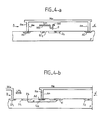
- One such embodiment is shown in Figure 1.
- FIG. 1 In this top view of the circuit, there are two lines of metal, which represent the impact on the substrate of the vertical fallout of metal. These lines are shown, in FIG. 1, by an area delimited in bold lines.
- the object of the invention is to solve these drawbacks, by proposing a different cell structure, which allows on the one hand, to produce a ring made up of metal fallout which is continuous around the cell and on the other hand, to reduce considerably the surface dimension of the UUPROM cell thus obtained.
- the present invention therefore relates to an integrated circuit produced in MOS technology from a semiconductor of a first type of doping, comprising at least one memory cell with floating gate having a source, a drain and a control gate. and protected from ultra-violet rays by a metal mask which covers it on an upper surface, this mask having anchoring points on the semiconductor substrate produced by metal fallout from the metal mask, characterized in that the memory cell with floating gate to a control gate produced by a diffusion of the second type of doping, and in that these anchoring points form a ring of continuous metal, anchored on a diffusion ring of the same type but more doped than the substrate and wider than the metal ring, this ring completely isolates the floating gate memory cell of the integrated circuit from ultraviolet rays, in an area inside the ring of metal and the drain, the source and the control grid being connected to the outside of the ring Am by buried connections.
- Figure 2 is a top plan view of an integrated circuit area protected from ultraviolet rays, according to an embodiment of the invention.
- the surface of the metal ring Am is entirely included in the surface of a diffusion ring Ad.
- the two extreme edges which delimit the width of the diffusion ring Ad are parallel to the borders extremes of the ring Am it contains: the ring Ad has the same shape as the ring Am it contains.
- the ring Ad is bordered by a limit border B1 on its external extreme border, its internal extreme border delimiting the internal zone 1.
- border F the set consisting of the rings Am and Ad and the border Bl. And we take for example a substrate of type P.
- a well N Ca1 is delimited by a parallelogram.
- the border F crosses it, parallel to two sides of the parallelogram, in top view.
- the parallelogram of the box Ca1 is a rectangle, the 2 sides of the greatest length being parallel to the border which crosses the box Ca1.
- the mediator on the sides of the box Ca1 parallel to the border is merged with the perpendicular bisector M of the segment XX ′, which is also the axis of symmetry M of the circuit in this exemplary embodiment according to the invention.
- the box Ca1 is delimited by fringed lines.
- a diffused zone Z1 N+ is delimited by a parallelogram.
- a metal contact AG is made over a whole part of the outer end at the border F of the diffused zone Z1.
- AG is the ordered mass of a not shown memory plane containing cells C1 and C2.
- this parallelogram is rectangular.
- the two sides of the longest length of the diffusion Z1 are parallel to those of the longest length of the box Ca1. They are also shorter; their perpendicular bisector is confused with the axis M of symmetry.
- a portion 10 of a diffused zone N+ Z2 is of the same shape, of equal and parallel greater length than the diffused zone Z1 opposite.
- the scattered zone Z2 is symmetrical with respect to the axis M.
- the part 1O is extended by an oblique narrowing 2O of symmetry M towards a new parallelogram 3O of symmetry M.
- This last part 3O of the diffused zone Z2 is continued by a zone diffused N+ which extends, over its greatest length, perpendicular to the axis M and symmetrically on either side of it: to the left of the axis M, it is the source S1 of the cell C1; on the right, it is the source S2 of cell C2.
- this arrangement makes it possible to connect the source S1 and the source S2 to the controlled ground AG by a single conductive link materialized by the zone Z2, by the box Ca1, by zone Z1, and finally by the metal contact by which the commanded ground signal AG is transmitted (for Array Ground, in Anglo-Saxon literature).
- this conductive link thus materialized is in fact the meeting of two conductive links, each of the links being in particular of sufficient width for the current draw on each of the sources S1 and S2.
- the memory cell C1 has a source zone S1 and a drain zone D1 which are diffusions N+, a floating grid GF1 produced in the form of a poly-silicon region and a control grid GC1 which is a diffusion N+ in l 'invention.
- branch 100 of the floating grid GF1.
- the axis of the longest branch 100 is vertical. Aligned in the horizontal axis of the longest length of the area S1, to the left of the branch 100, there is the diffused area N+ of the drain D1 of the cell C1. To the left of this area D1, another branch 200 of the floating gate GF1 passes over the area D1 perpendicular to its greatest length (ie vertically in the description).
- the branch 200 has the same shape in the plane of Figure 2 as the branch 100, but it is narrower.
- the diffusion zone D1 continues into another zone of diffusion N+ Z3, which leaves vertically upwards, then quickly in a left oblique direction towards the top of the interior zone 1.
- This zone Z3 ends in a parallelogram 11, preferably rectangular.
- the diffusion Z3, in this part 11 is carried out astride the substrate of the interior zone and a box Ca2.
- the Ca2 box is preferably rectangular; its two longer sides are parallel to those of the parallelogram 11 of the zone Z3 opposite and longer.
- the Ca2 box is crossed by the vertical left side of the border, parallel to its two longer sides.
- N + Z4 diffusion is produced in the same shape and of equal greater length than the part 11 of the Z3 diffusion, which is opposite.
- This diffusion Z4 has a narrower left part which also forms a parallelogram and which produces the source St1 of the selection transistor TS1.
- This diffused part St1 is cut to the left and perpendicularly by a poly-silicon region which produces the control gate Gt1 of the selection transistor and which carries a word line signal LM1.
- This poly-silicon region cuts to the left and perpendicularly the drain diffusion zone Dt1 of the transistor TS1, zone Dt1 which is opposite that of the source St1. On this diffusion zone Dt1, a metal contact is made. This metal contact transmits a bit line signal LB1 to the drain Dt1 of the selection transistor TS1.
- the diffusion zone Z3 indirectly through the well Ca2 and the diffusion zone Z4, contacts the drain D1 of the cell C1, at the source St1 of selection transistor TS1 ( Figure 3).
- the zone D1 indeed extends as we have seen by the diffusion zone Z3.
- the branch 200 of the floating gate GF1 moreover approaches a location on the substrate, thereby reducing the oxide thickness at this location and in particular near the drain D1: this region of smaller oxide thickness (for example 90 Angstroms) is called the tunnel oxide region O ( Figures 4.d, 4.a). It promotes the transfer of charges between the drain D1 and the floating gate GF1.
- the two branches 100 and 200 join at their lower end a parallelogram 300 placed lower than the aligned areas of the source S1 and the drain D1 of the cell C1.
- This part 300 of the grid GF1 covers an N + Z5 diffusion which realizes under this floating grid, the control grid GC1.
- the diffusion Z5 extends to the left, towards the border where it ends straddling the substrate of the interior zone 1 and a well N Ca4 made on both sides and under the border, like the wells Ca1 and Ca2 already seen.
- the border crosses the Ca4 box parallel to one of its sides.
- This Ca4 box is preferably a parallelogram. These are the shortest sides which are, this time, those parallel to the border.
- the signals AG, LB1, LM1 and CG1 are the 4 control signals associated with the selection transistor TS1, and with the memory cell C1; by their state, they control a reading, a programming or an erasure of the cell C1.
- An example of the states corresponding to a reading, programming or deletion are given in the following table: Vss is the electrical ground of the circuit to which the metal mask and therefore also the diffusion ring Ad.
- the contact-making diffusion ring Ad is advantageously wider than the ring Am which it contains entirely.
- the vertical fallout is for example obtained, by digging the circuit to the substrate, according to well known technological methods. Holes are then formed, the bottom of which is formed by the surface of the substrate.
- the exposed surface of the substrate must not be wider than the contact surface diffusion on the surface of the substrate, because otherwise the metal may come into contact, not only on this diffusion, but also on the part and other of this diffusion, with the risks of short circuit that this entails.
- the boundary border Bl represents the projection of the contours of the metal mask, in the plane of FIG. 2.
- the metal mask Mm overflows from the vertical metal fallout Rm. This makes it possible to reliably ensure that the metal layer, when it is going to be applied, will fill all the holes to the bottom, that is to say to the surface of the substrate. Since the metal layer is spread out, it is in fact preferable to have a flat surface on either side of the hole.
- the memory cell C1 has a floating grid GF1 and a control grid GC1.
- its control grid is a diffusion and not a poly-silicon grid as for UUPROM cells in the prior art. Indeed, a cell having its diffusion control grid and its floating poly-silicon grid is substantially larger than a cell with two levels of poly-silicon (floating grid and control grid).
- the control grid GC1 in diffusion is offset in the plane, relative to the source regions S1 and drain D1, the floating grid then covering the source and drain regions on the one hand and the control grid of somewhere else.
- the control grid covers the floating grid, which itself covers the source and drain regions.
- An EEPROM cell is necessarily controlled by a selection transistor, since we want to have at least two of the three commands that are the reading, programming and erasing of the cell.
- the electrical diagram corresponding to FIG. 2 is given in FIG. 3.
- the selection transistor TS1 and the memory cell C1 are of the same type channel, opposite to the type of doping of the substrate.
- the description which is made with a substrate P is easily transposable to a substrate of type N, by reversing the type of impurities and the polarization in the description.
- the EEPROM cell is, in the example, non-symmetrical: the drain D1 and the source S1 are not interchangeable.
- the drain D1 is in fact particularized by a region of thin oxide O, under the branch 200 of the floating gate GF1, which facilitates the transfer of the charges by tunnel effect. This is what is represented in section DD ′ in FIG. 4d, with the tunnel oxide zone O under the branch 200 of the floating grid GF1.
- Diffusion N+ of the control grid GC1 is carried out before the poly-silicon region 300, above it. Diffusion N+ is then very present under the floating grid, as can be seen in sections AA′ and CC ′ of FIGS. 4a and 4c respectively.
- this second diffusion is how the metal contact associated with the control grid control CG1 is made.
- This second possible embodiment is shown in section in FIG. 4c. It all depends on the topology of the circuitry which generates CG1 for example. Thus if the signal CG1 is generated far from the UUPROM cell, it will be brought to it by a metal line: we will then make the metal contact directly on the Ca4 box in the example.
- the signal CG1 comes from a transistor very close to the UUPROM cell, it will arrive in diffusion N diffusion and a contact N+, on the box will be necessary: this is the case in the example of the box Ca2 for the signal St1.
- These metal contacts are made outside the border. If they were indeed made inside the border, it would be necessary to cross the metal conductor which carries a control signal, either the metal mask, or the fallout Rm of this metal mask which are set to the potential of mass Vss: a short circuit would be caused.
- the ratio of the width l separating two N+ diffusions on either side of a box at the border, at the longest length L of these N+ diffusions parallel to the border, is made as small as possible , while respecting the drawing rules, so as to reduce as much as possible the resistance induced R by the well N.
- the resistivity p of the well N is higher than that of a diffusion N+, because the resistivity of diffusion is inversely proportional to the doping rate.
- an optimum l / L ratio is preferably chosen for a minimum induced resistance.
- the diffusions for the buried connections linked to the signal AG and to the source St1 of the selection transistor are made in the example.
- this selection transistor TS1 is preferably placed outside this perimeter because its control gate is made of poly-silicon. This is not annoying otherwise, because it is not to be protected from ultraviolet rays.
- This solution however has many drawbacks.
- the selection transistor TS1 then has the two control line signals LB1 and LM1, which are transmitted via a box under the border, which degrades the access time to the transistor and therefore to the cell.
- the metal contact between the control grid and an N+ distribution should be made by a metal line, located in a plane above the control grid, this metal line having at its two ends two fallouts, one on the grid, one on the broadcast.
- the metal line could not be in the plane of the metal mask, there would therefore be a second metal plane included between the first metal plane of the metal mask and the control grid.
- the multiplicity of contacts and modes of conduction tends to increase the access time (conduction via a box, metal contact between an N+ diffusion and a poly-silicon region).
- the metal fallout it is not important for the metal fallout to be vertical: this is a characteristic which only follows from the example of the process for obtaining this fallout described. It is only necessary that these fallouts connect the metal mask to the substrate and that they are anchored continuously on a diffusion of the substrate, so as to completely isolate the interior area from ultraviolet rays.
- the cells C1 and C2 have in the example, their source S1 and S2 at the same commanded mass signal AG: this signal is in fact common to the whole memory plane and the cells C1 and C2 are independent.
- Other configurations are possible, depending on the logic function to be performed.
- the area occupied by two memory cells protected from ultraviolet rays according to the invention has been reduced by twice the area of a ring line Ad along the axis M, relative to the area occupied by two memory cells each protected independently of the ultraviolet rays according to the invention.
Landscapes
- Semiconductor Memories (AREA)
- Non-Volatile Memory (AREA)
Applications Claiming Priority (2)
| Application Number | Priority Date | Filing Date | Title |
|---|---|---|---|
| FR8916649 | 1989-12-14 | ||
| FR8916649A FR2656156A1 (fr) | 1989-12-16 | 1989-12-16 | Circuit integre entierement protege des rayons ultra-violets. |
Publications (2)
| Publication Number | Publication Date |
|---|---|
| EP0433174A1 true EP0433174A1 (de) | 1991-06-19 |
| EP0433174B1 EP0433174B1 (de) | 1992-06-03 |
Family
ID=9388578
Family Applications (1)
| Application Number | Title | Priority Date | Filing Date |
|---|---|---|---|
| EP90403570A Expired - Lifetime EP0433174B1 (de) | 1989-12-15 | 1990-12-13 | Integrierte Schaltung mit vollständigem Schutz gegen Ultraviolettstrahlen |
Country Status (4)
| Country | Link |
|---|---|
| US (1) | US5235541A (de) |
| EP (1) | EP0433174B1 (de) |
| DE (1) | DE69000129T2 (de) |
| FR (1) | FR2656156A1 (de) |
Cited By (2)
| Publication number | Priority date | Publication date | Assignee | Title |
|---|---|---|---|---|
| DE4305849A1 (en) * | 1992-02-28 | 1993-09-02 | Mitsubishi Electric Corp | Non-volatile storage device - comprises storage cell and central storage unit having UV impermeable resin layer |
| EP0576773A1 (de) * | 1992-06-30 | 1994-01-05 | STMicroelectronics S.r.l. | Integrierte Schaltung mit vollständigem Schutz gegen Ultraviolettstrahlen |
Families Citing this family (9)
| Publication number | Priority date | Publication date | Assignee | Title |
|---|---|---|---|---|
| AT401656B (de) * | 1994-11-07 | 1996-11-25 | Chemiefaser Lenzing Ag | Flammfestes nicht gewebtes textiles gebilde |
| KR970054309A (ko) * | 1995-12-29 | 1997-07-31 | 김주용 | 불 휘발성 반도체 메모리장치 |
| US5719427A (en) * | 1997-01-14 | 1998-02-17 | Pericom Semiconductor Corp. | Avalanche-enhanced CMOS transistor for EPROM/EEPROM and ESD-protection structures |
| GB2341272B (en) | 1998-09-03 | 2003-08-20 | Ericsson Telefon Ab L M | High voltage shield |
| US7339835B1 (en) * | 2005-02-14 | 2008-03-04 | National Semiconductor Corporation | Non-volatile memory structure and erase method with floating gate voltage control |
| KR20070103069A (ko) * | 2005-02-15 | 2007-10-22 | 알피오 피티와이 리미티드 | 중합체 물질의 포토리소그래픽 패턴화 |
| US9406621B2 (en) | 2010-06-10 | 2016-08-02 | Texas Instruments Incorporated | Ultraviolet energy shield for non-volatile charge storage memory |
| CN102314036A (zh) * | 2010-06-29 | 2012-01-11 | 普诚科技股份有限公司 | 抗紫外光的电子装置及其制法 |
| CN114054925A (zh) * | 2021-11-10 | 2022-02-18 | 合肥维信诺科技有限公司 | 一种掩膜板的制作方法 |
Citations (3)
| Publication number | Priority date | Publication date | Assignee | Title |
|---|---|---|---|---|
| EP0044384A2 (de) * | 1980-06-30 | 1982-01-27 | International Business Machines Corporation | Elektrisch veränderliche Festspeicherzelle |
| US4519050A (en) * | 1982-06-17 | 1985-05-21 | Intel Corporation | Radiation shield for an integrated circuit memory with redundant elements |
| EP0227549A2 (de) * | 1985-12-18 | 1987-07-01 | Fujitsu Limited | Halbleiterspeicheranordnung mit einem Nurlesespeicherelement zum Speichern von bestimmter Information |
Family Cites Families (9)
| Publication number | Priority date | Publication date | Assignee | Title |
|---|---|---|---|---|
| US4530074A (en) * | 1982-06-17 | 1985-07-16 | Intel Corporation | Radiation shield for a portion of a radiation sensitive integrated circuit |
| JPS596581A (ja) * | 1982-07-02 | 1984-01-13 | Mitsubishi Electric Corp | 半導体不揮発性記憶装置 |
| US4577295A (en) * | 1983-05-31 | 1986-03-18 | Intel Corporation | Hybrid E2 cell and related array |
| US4805138A (en) * | 1985-08-23 | 1989-02-14 | Texas Instruments Incorporated | An unerasable eprom cell |
| US5034786A (en) * | 1986-08-29 | 1991-07-23 | Waferscale Integration, Inc. | Opaque cover for preventing erasure of an EPROM |
| US4758869A (en) * | 1986-08-29 | 1988-07-19 | Waferscale Integration, Inc. | Nonvolatile floating gate transistor structure |
| US4970565A (en) * | 1988-09-01 | 1990-11-13 | Atmel Corporation | Sealed charge storage structure |
| US5086410A (en) * | 1990-09-14 | 1992-02-04 | National Semiconductor Corporation | Non-erasable eprom cell for redundancy circuit |
| US5050123A (en) * | 1990-11-13 | 1991-09-17 | Intel Corporation | Radiation shield for EPROM cells |
-
1989
- 1989-12-16 FR FR8916649A patent/FR2656156A1/fr not_active Withdrawn
-
1990
- 1990-12-13 DE DE9090403570T patent/DE69000129T2/de not_active Expired - Lifetime
- 1990-12-13 EP EP90403570A patent/EP0433174B1/de not_active Expired - Lifetime
- 1990-12-14 US US07/627,829 patent/US5235541A/en not_active Expired - Lifetime
Patent Citations (3)
| Publication number | Priority date | Publication date | Assignee | Title |
|---|---|---|---|---|
| EP0044384A2 (de) * | 1980-06-30 | 1982-01-27 | International Business Machines Corporation | Elektrisch veränderliche Festspeicherzelle |
| US4519050A (en) * | 1982-06-17 | 1985-05-21 | Intel Corporation | Radiation shield for an integrated circuit memory with redundant elements |
| EP0227549A2 (de) * | 1985-12-18 | 1987-07-01 | Fujitsu Limited | Halbleiterspeicheranordnung mit einem Nurlesespeicherelement zum Speichern von bestimmter Information |
Non-Patent Citations (1)
| Title |
|---|
| PATENT ABSTRACTS OF JAPAN, vol. 8, no. 88 (E-240)[1525], 21 avril 1984; & JP-A-59 6581 (MITSUBISHI DENKI K.K.) 13-01-1984 * |
Cited By (4)
| Publication number | Priority date | Publication date | Assignee | Title |
|---|---|---|---|---|
| DE4305849A1 (en) * | 1992-02-28 | 1993-09-02 | Mitsubishi Electric Corp | Non-volatile storage device - comprises storage cell and central storage unit having UV impermeable resin layer |
| US5519246A (en) * | 1992-02-28 | 1996-05-21 | Mitsubishi Denki Kabushiki Kaisha | Nonvolatile memory apparatus using an ultraviolet impermeable resin film |
| EP0576773A1 (de) * | 1992-06-30 | 1994-01-05 | STMicroelectronics S.r.l. | Integrierte Schaltung mit vollständigem Schutz gegen Ultraviolettstrahlen |
| US5440510A (en) * | 1992-06-30 | 1995-08-08 | Sgs-Thomson Microelectronics, S.R.L. | Integrated circuit entirely protected against ultraviolet rays |
Also Published As
| Publication number | Publication date |
|---|---|
| DE69000129D1 (de) | 1992-07-09 |
| EP0433174B1 (de) | 1992-06-03 |
| DE69000129T2 (de) | 1992-12-17 |
| US5235541A (en) | 1993-08-10 |
| FR2656156A1 (fr) | 1991-06-21 |
Similar Documents
| Publication | Publication Date | Title |
|---|---|---|
| EP2304794B1 (de) | Struktur und verfahren zur herstellung einer mikroelektronischen 3d-nand-flash-speichervorrichtung | |
| FR2670316A1 (fr) | Procede de fabrication d'un dispositif de memoire morte a masque. | |
| EP1495496B1 (de) | Elektrisch löschbare und programmiebare nichtflüchtige halbleiterspeicheranordnung mit einschichtigem gatematerial und entsprechende speicherfläche | |
| EP0433174B1 (de) | Integrierte Schaltung mit vollständigem Schutz gegen Ultraviolettstrahlen | |
| FR2692720A1 (fr) | Dispositif d'EPROM à couche unique de silicium polycristallin à effacement rapide. | |
| EP0354859B1 (de) | Hochintegrierte EPROM-Speicheranordnung mit einer quadratischen Gitterorganisation und mit einem verbesserten Kopplungsfaktor | |
| FR2879800A1 (fr) | Dispositif a memoire integree et procede | |
| EP0648375B1 (de) | Flash-eeprom-speicher mit drei gateelektroden und sein herstellungsverfahren. | |
| FR2725309A1 (fr) | Dispositif memoire non volatile a semi-conducteurs et procede de fabrication de celui-ci | |
| FR2494042A1 (fr) | Dispositifs a semiconducteurs et procede pour fabriquer ces derniers | |
| FR2763425A1 (fr) | Dispositif a semiconducteurs ayant une grille en silicium polycristallin contenant une impurete de dopage et de l'azote, et procede de fabrication | |
| FR2858717A1 (fr) | Procede de fabrication d'une cellule auto-alignee du type silicium-oxyde-nitrure-oxyde-silicium et cette cellule | |
| FR3084771A1 (fr) | Element anti-fusible compact et procede de fabrication | |
| EP0354858B1 (de) | Hochintegrierte EPROM-Speicheranordnung mit einem grossen Kopplungsfaktor | |
| EP0356346B1 (de) | Hochintegrierte EPROM-Speicheranordnung | |
| FR2767219A1 (fr) | Dispositif memoire non volatile programmable et effacable electriquement compatible avec un procede de fabrication cmos/soi | |
| WO1988002172A2 (fr) | Memoire non-volatile a grille flottante sans oxyde epais | |
| FR3085530A1 (fr) | Circuit integre comportant au moins une cellule memoire avec un dispositif anti-fusible. | |
| FR2549274A1 (fr) | Cellule de memoire vive dynamique a rendement eleve et procede de fabrication | |
| FR3000838A1 (fr) | Procede de fabrication d’une memoire non volatile | |
| EP1187142B1 (de) | Zwischenspeicherzelle mit Maskierung und gleicher Anzahl von N-Kanal Transistoren und P-Kanal Transistoren | |
| EP3890024B1 (de) | Elektronischer chip mit zwei phasenwechselspeichern und herstellungsverfahren | |
| FR2543738A1 (fr) | Procede pour l'auto-alignement d'une double couche de silicium polycristallin, dans un dispositif a circuit integre, au moyen d'une operation d'oxydation | |
| EP0298829B1 (de) | Verfahren zum Einstellen des Leitungszustandes eines MOS-Transistors | |
| FR2826779A1 (fr) | Contact antistatique pour ligne en silicium polycristallin |
Legal Events
| Date | Code | Title | Description |
|---|---|---|---|
| PUAI | Public reference made under article 153(3) epc to a published international application that has entered the european phase |
Free format text: ORIGINAL CODE: 0009012 |
|
| AK | Designated contracting states |
Kind code of ref document: A1 Designated state(s): DE FR GB IT |
|
| 17P | Request for examination filed |
Effective date: 19910605 |
|
| 17Q | First examination report despatched |
Effective date: 19911014 |
|
| GRAA | (expected) grant |
Free format text: ORIGINAL CODE: 0009210 |
|
| AK | Designated contracting states |
Kind code of ref document: B1 Designated state(s): DE FR GB IT |
|
| ITF | It: translation for a ep patent filed | ||
| REF | Corresponds to: |
Ref document number: 69000129 Country of ref document: DE Date of ref document: 19920709 |
|
| GBT | Gb: translation of ep patent filed (gb section 77(6)(a)/1977) | ||
| PLBE | No opposition filed within time limit |
Free format text: ORIGINAL CODE: 0009261 |
|
| STAA | Information on the status of an ep patent application or granted ep patent |
Free format text: STATUS: NO OPPOSITION FILED WITHIN TIME LIMIT |
|
| 26N | No opposition filed | ||
| REG | Reference to a national code |
Ref country code: FR Ref legal event code: D6 |
|
| REG | Reference to a national code |
Ref country code: GB Ref legal event code: IF02 |
|
| PGFP | Annual fee paid to national office [announced via postgrant information from national office to epo] |
Ref country code: FR Payment date: 20021210 Year of fee payment: 13 |
|
| PGFP | Annual fee paid to national office [announced via postgrant information from national office to epo] |
Ref country code: GB Payment date: 20021211 Year of fee payment: 13 |
|
| PGFP | Annual fee paid to national office [announced via postgrant information from national office to epo] |
Ref country code: DE Payment date: 20021219 Year of fee payment: 13 |
|
| PG25 | Lapsed in a contracting state [announced via postgrant information from national office to epo] |
Ref country code: GB Free format text: LAPSE BECAUSE OF NON-PAYMENT OF DUE FEES Effective date: 20031213 |
|
| PG25 | Lapsed in a contracting state [announced via postgrant information from national office to epo] |
Ref country code: DE Free format text: LAPSE BECAUSE OF NON-PAYMENT OF DUE FEES Effective date: 20040701 |
|
| GBPC | Gb: european patent ceased through non-payment of renewal fee |
Effective date: 20031213 |
|
| PG25 | Lapsed in a contracting state [announced via postgrant information from national office to epo] |
Ref country code: FR Free format text: LAPSE BECAUSE OF NON-PAYMENT OF DUE FEES Effective date: 20040831 |
|
| REG | Reference to a national code |
Ref country code: FR Ref legal event code: ST |
|
| PG25 | Lapsed in a contracting state [announced via postgrant information from national office to epo] |
Ref country code: IT Free format text: LAPSE BECAUSE OF NON-PAYMENT OF DUE FEES;WARNING: LAPSES OF ITALIAN PATENTS WITH EFFECTIVE DATE BEFORE 2007 MAY HAVE OCCURRED AT ANY TIME BEFORE 2007. THE CORRECT EFFECTIVE DATE MAY BE DIFFERENT FROM THE ONE RECORDED. Effective date: 20051213 |