EP1495496B1 - Elektrisch löschbare und programmiebare nichtflüchtige halbleiterspeicheranordnung mit einschichtigem gatematerial und entsprechende speicherfläche - Google Patents
Elektrisch löschbare und programmiebare nichtflüchtige halbleiterspeicheranordnung mit einschichtigem gatematerial und entsprechende speicherfläche Download PDFInfo
- Publication number
- EP1495496B1 EP1495496B1 EP03709915A EP03709915A EP1495496B1 EP 1495496 B1 EP1495496 B1 EP 1495496B1 EP 03709915 A EP03709915 A EP 03709915A EP 03709915 A EP03709915 A EP 03709915A EP 1495496 B1 EP1495496 B1 EP 1495496B1
- Authority
- EP
- European Patent Office
- Prior art keywords
- transistor
- gate
- memory cell
- memory
- zone
- Prior art date
- Legal status (The legal status is an assumption and is not a legal conclusion. Google has not performed a legal analysis and makes no representation as to the accuracy of the status listed.)
- Expired - Lifetime
Links
- 239000000463 material Substances 0.000 title claims abstract description 47
- 239000004065 semiconductor Substances 0.000 title claims abstract description 15
- 239000000758 substrate Substances 0.000 claims abstract description 61
- 238000002955 isolation Methods 0.000 claims abstract description 14
- 239000010410 layer Substances 0.000 claims description 33
- 238000001465 metallisation Methods 0.000 claims description 20
- 101150067766 mpl2 gene Proteins 0.000 claims description 17
- 239000002784 hot electron Substances 0.000 claims description 13
- 101100238358 Dictyostelium discoideum mpl3 gene Proteins 0.000 claims description 10
- 239000002356 single layer Substances 0.000 claims description 3
- 101150116173 ver-1 gene Proteins 0.000 claims description 3
- 101150011281 mpl1 gene Proteins 0.000 claims 1
- 230000010287 polarization Effects 0.000 abstract description 19
- 238000009413 insulation Methods 0.000 description 10
- 230000008878 coupling Effects 0.000 description 7
- 238000010168 coupling process Methods 0.000 description 7
- 238000005859 coupling reaction Methods 0.000 description 7
- 238000004519 manufacturing process Methods 0.000 description 6
- 230000014759 maintenance of location Effects 0.000 description 5
- 230000015556 catabolic process Effects 0.000 description 4
- 238000006731 degradation reaction Methods 0.000 description 4
- 230000005684 electric field Effects 0.000 description 4
- 238000002513 implantation Methods 0.000 description 4
- 230000008672 reprogramming Effects 0.000 description 4
- 230000032683 aging Effects 0.000 description 3
- 230000008901 benefit Effects 0.000 description 3
- 229910021420 polycrystalline silicon Inorganic materials 0.000 description 3
- 229920005591 polysilicon Polymers 0.000 description 3
- CURLTUGMZLYLDI-UHFFFAOYSA-N Carbon dioxide Chemical compound O=C=O CURLTUGMZLYLDI-UHFFFAOYSA-N 0.000 description 2
- VYPSYNLAJGMNEJ-UHFFFAOYSA-N Silicium dioxide Chemical compound O=[Si]=O VYPSYNLAJGMNEJ-UHFFFAOYSA-N 0.000 description 2
- XUIMIQQOPSSXEZ-UHFFFAOYSA-N Silicon Chemical compound [Si] XUIMIQQOPSSXEZ-UHFFFAOYSA-N 0.000 description 2
- 239000000969 carrier Substances 0.000 description 2
- 238000010292 electrical insulation Methods 0.000 description 2
- 229910052710 silicon Inorganic materials 0.000 description 2
- 239000010703 silicon Substances 0.000 description 2
- 241000451680 Buxus natalensis Species 0.000 description 1
- 230000004888 barrier function Effects 0.000 description 1
- 230000000903 blocking effect Effects 0.000 description 1
- 229910002092 carbon dioxide Inorganic materials 0.000 description 1
- 239000001569 carbon dioxide Substances 0.000 description 1
- 239000013078 crystal Substances 0.000 description 1
- 238000012217 deletion Methods 0.000 description 1
- 230000037430 deletion Effects 0.000 description 1
- 238000001514 detection method Methods 0.000 description 1
- 239000003989 dielectric material Substances 0.000 description 1
- 238000009792 diffusion process Methods 0.000 description 1
- 230000000694 effects Effects 0.000 description 1
- 230000006870 function Effects 0.000 description 1
- 238000000034 method Methods 0.000 description 1
- 230000008569 process Effects 0.000 description 1
- 230000000284 resting effect Effects 0.000 description 1
- 235000012239 silicon dioxide Nutrition 0.000 description 1
- 239000000377 silicon dioxide Substances 0.000 description 1
- 241000894007 species Species 0.000 description 1
Images







Classifications
-
- H—ELECTRICITY
- H10—SEMICONDUCTOR DEVICES; ELECTRIC SOLID-STATE DEVICES NOT OTHERWISE PROVIDED FOR
- H10B—ELECTRONIC MEMORY DEVICES
- H10B41/00—Electrically erasable-and-programmable ROM [EEPROM] devices comprising floating gates
- H10B41/30—Electrically erasable-and-programmable ROM [EEPROM] devices comprising floating gates characterised by the memory core region
-
- H—ELECTRICITY
- H10—SEMICONDUCTOR DEVICES; ELECTRIC SOLID-STATE DEVICES NOT OTHERWISE PROVIDED FOR
- H10B—ELECTRONIC MEMORY DEVICES
- H10B41/00—Electrically erasable-and-programmable ROM [EEPROM] devices comprising floating gates
- H10B41/60—Electrically erasable-and-programmable ROM [EEPROM] devices comprising floating gates the control gate being a doped region, e.g. single-poly memory cell
-
- H—ELECTRICITY
- H10—SEMICONDUCTOR DEVICES; ELECTRIC SOLID-STATE DEVICES NOT OTHERWISE PROVIDED FOR
- H10B—ELECTRONIC MEMORY DEVICES
- H10B69/00—Erasable-and-programmable ROM [EPROM] devices not provided for in groups H10B41/00 - H10B63/00, e.g. ultraviolet erasable-and-programmable ROM [UVEPROM] devices
-
- H—ELECTRICITY
- H10—SEMICONDUCTOR DEVICES; ELECTRIC SOLID-STATE DEVICES NOT OTHERWISE PROVIDED FOR
- H10D—INORGANIC ELECTRIC SEMICONDUCTOR DEVICES
- H10D30/00—Field-effect transistors [FET]
- H10D30/01—Manufacture or treatment
- H10D30/021—Manufacture or treatment of FETs having insulated gates [IGFET]
- H10D30/0411—Manufacture or treatment of FETs having insulated gates [IGFET] of FETs having floating gates
-
- H—ELECTRICITY
- H10—SEMICONDUCTOR DEVICES; ELECTRIC SOLID-STATE DEVICES NOT OTHERWISE PROVIDED FOR
- H10D—INORGANIC ELECTRIC SEMICONDUCTOR DEVICES
- H10D30/00—Field-effect transistors [FET]
- H10D30/60—Insulated-gate field-effect transistors [IGFET]
- H10D30/68—Floating-gate IGFETs
- H10D30/681—Floating-gate IGFETs having only two programming levels
Definitions
- the invention relates to integrated circuits, and more particularly to semiconductor memory devices of the nonvolatile type, programmable and electrically erasable to a single layer of gate material.
- Such a memory point is well known to those skilled in the art.
- US Patent No. 5,761,121 give an example for a PMOS structure. More specifically, such a cell comprises a floating gate transistor and a control gate which is implemented by implantation within a semiconductor substrate. This buried layer, which acts as a control gate, is capacitively coupled to the floating gate. The control gate and the floating gate transistor are electrically isolated by an insulating zone, for example of the shallow trench type (STI: "Shallow Trench Isolation").
- STI shallow trench type
- the gate material layer generally polysilicon, in which is formed the floating gate of the transistor, is isolated from the active area by a dielectric, for example silicon dioxide.
- the invention aims to provide a solution to this problem.
- the purpose of the invention is to propose a memory cell structure that avoids the aging phenomenon of the transistor during repeated erase cycles.
- the invention also aims to allow programming of the cell, either by programming of the type "hot carriers” or by a programming of the type "Fowler-Nordheim".
- the invention also aims to provide such a memory whose manufacturing process is fully compatible with a conventional CMOS manufacturing process.
- the invention therefore proposes a semiconductor memory device, comprising a non-volatile, programmable and electrically erasable memory cell, with a single layer of gate material, and comprising a floating gate transistor and a control gate.
- the source, drain and channel regions of the floating gate transistor form the control gate.
- the memory cell comprises a dielectric zone disposed between a first portion of the gate material layer and a first electrically insulated first active area of a second active zone incorporating the control gate. This dielectric zone then forms a "tunnel" zone for, during an erasure of the cell, to allow the transfer to the first active zone of the charges stored in the floating gate.
- the channel region here is understood to be the semiconductor region extending between the source region and the drain region under the gate of the transistor.
- the structure of the memory cell is therefore totally different from the conventional structures in that it does not have a separate control gate of the floating gate transistor. Indeed, according to the invention, it is a part of the floating gate transistor, and more particularly the source, drain and channel regions of this transistor, which form the control gate.
- the evacuation of the charges during an erasure of the cell takes place through, not the gate oxide of the floating gate transistor, but through a gate oxide (dielectric material) which is located in view of an electrically isolated active area of the active area incorporating the control gate, and therefore the source, channel and drain regions of the floating gate transistor. Consequently, the degradation of the oxide of the tunnel zone according to the invention does not cause aging of the transistor of the cell.
- the fact that the source, drain and channel regions of the transistor form the control gate and that the tunnel zone situated opposite said first active zone constitutes the charge transfer zone, is linked to the fact that the capacitive coupling between the second and the second active zone (that in which the source, drain and channel regions of the transistor are formed) and the floating gate, is more important than the capacitive coupling at the tunnel zone.
- the different capacitive couplings depend on the gate material surfaces facing the active areas as well as the different voltages applied to the different electrodes of the memory cell. Those skilled in the art will be able to adjust these different parameters to obtain the desired effect.
- a capacitive value of the tunnel zone of less than or equal to 30% of the total capacitive value between the layer of gate material and the set of active areas of the memory cell.
- the transistor has an annular gate and the gate material layer comprises, in addition to the annular gate and said first portion, a connecting portion between this first portion and the annular gate.
- the first active zone and the second active zone can be electrically insulated from each other at depth by PN junctions intended to be reverse-biased, and at the surface by a region of FIG. insulation, for example a shallow trench type insulation region.
- the first active zone is formed in a first substrate region (for example a box) having a first conductivity type, for example the type of conductivity N.
- the second active zone is realized in a second substrate region (for example a box) also having the first type of conductivity.
- the first substrate region and the second substrate region are then separated by a third substrate region (for example another well) having a second conductivity type different from the first, for example the conductivity type P.
- the isolation region extends between the first substrate region and the second substrate region and then comprises an orifice opening on a contacting zone (P + zone for example) of the third semiconductor region.
- the first active zone and the second active zone may be electrically isolated from each other solely by PN junctions intended to be reverse biased.
- Such an embodiment makes it possible to obtain better data retention. Indeed, it was observed that it was necessary to choose a thickness of the dielectric greater than 60 ⁇ , so as to obtain good data retention. However, it has been observed that a thinning of the gate dielectric occurs at the interface between the insulation zone, for example of the shallow trench type, and the gate material. And, this leads to less good data retention. Therefore, the embodiment which provides for no overlapping of the isolation region by the gate material layer solves this problem.
- the gate material layer extends integrally over the above-mentioned three substrate regions, without overlapping isolation region.
- the first substrate region has on the surface a contacting zone having the first conductivity type, for example an N + type contact zone in an N. box.
- a surface zone having the second conductivity type for example the P + type, and extending around said tunnel zone.
- this surface area is electrically connected to the contact area, for example by siliciding.
- the device furthermore comprises polarization means having a programming state of the memory cell, a read state of the memory cell and an erase state of the memory cell. .
- the polarization means causes a Fowler-Nordheim type erasure, by applying a voltage on the first active zone that is much higher than the voltages applied to the source, drain and substrate regions of the transistor. .
- the biasing means in the erase state, preferably apply equal voltages to the source, drain and substrate regions of the transistor.
- the biasing means may cause hot carrier programming at the transistor.
- They can also cause programming of the Fowler-Nordheim type, by applying to the source, drain and substrate regions of the transistor, voltages, preferably equal to, and much higher than those applied to the first active zone.
- a drain / source voltage difference limited to 1 volt in absolute value will be chosen. This makes it possible to avoid very slow reprogramming of the memory cell, or unwanted unwanted programming of a blank memory cell.
- the floating gate transistor is preferably a PMOS transistor. This being the case, the invention also applies to a transistor of the NMOS type.
- the device may comprise a memory plane comprising a plurality of memory cells.
- the device can thus form a memory of the EEPROM type or of the FLASH type.
- the invention also relates to an integrated circuit comprising a device as defined above.
- the figures 1a (respectively 2a and 3a) and 1b (respectively 2b, and 3b) are respectively sections along lines AA and BB of the figure 1 (respectively of the figure 2 and some figure 3 ).
- the reference SB denotes a semiconductor substrate, such as doped silicon P -, an integrated circuit.
- This substrate SB comprises a first substrate region RG1 formed of an N-doped semiconductor well, and a second substrate region RG2 formed of another N-doped semiconductor well.
- the two wells RG1 and RG2 are separated by a third region.
- semiconductor RG3 formed of a p-doped box.
- the RG3 casing provides mutual electrical isolation in depth of the two boxes RG1 and RG2. Indeed, this electrical insulation is achieved by PN junctions which will be polarized in reverse.
- the mutual electrical insulation of the two boxes RG1 and RG2 is provided by a STI insulation region, for example of the shallow trench type.
- the insulation region STI comprises an orifice opening on a P + doped P + contacting zone and situated on the surface of the RG3 box. This contact PSB will ensure a polarization of the box RG3 and also the underlying substrate SB.
- the box RG1 forms a first active zone, while the box RG2 forms a second active zone.
- a layer of a gate material for example polysilicon, resting on the surface of the two active zones via a gate oxide OX, for example carbon dioxide. silicon.
- a gate oxide OX for example carbon dioxide. silicon.
- the layer of gate material which as a whole forms a floating gate, has a first portion P1 overlooking the first active area RG1.
- the gate material layer also has an annular FG portion disposed above the second active area RG2.
- This annular portion of gate material defines the gate FG of a PMOS transistor, also called a charge storage or read transistor, whose source S, formed of a P + type implanted region, is located in the RG2 box. outside the annular gate, and the drain D also formed of a P + type implanted region, is located in the box RG2 inside the ring forming the gate FG.
- the gate material layer also has a connecting portion PL connecting the annular portion FG and the first portion P1.
- the geometry of the first portion P1 has been chosen so that the capacitive value of the oxide zone OX located under this first portion P1, and also called tunnel zone ZTN for reasons which will be explained in more detail below. , which is less than or equal to 30% of the total capacitive value between the layer of gate material and the set of active areas of the memory cell, that is to say the sum of the capacitances formed between the gate material and each of the active areas of the memory cell.
- the source, drain and channel regions, which are capacitively coupled to the gate FG, will form a control gate for this memory cell, while the tunnel area ZTN will form a transfer zone. loads enabling the evacuation of the charges stored in the floating gate to the first active zone RG1 during an erasing of the memory cell.
- control gate it is of course the channel zone which participates essentially in the capacitive coupling with the annular gate FG. That being so, those skilled in the art know that the source and drain regions also overflow by diffusion under the annular gate FG. Also, these source and drain regions also participate in practice in this capacitive coupling.
- the first active area RG1 In order to properly polarize the first active area RG1, it comprises an implanted area N + , referenced PC1, and allowing a contact.
- This surface zone ZS is electrically connected to the contacting zone PC1, for example by surface siliciding.
- the second active zone RG2 there is also provided an implanted region N + , referenced BK, allowing contacting and polarization of this box RG2, and therefore a polarization of the substrate of the read transistor.
- the manufacturing method of such a memory cell comprises, first of all, the realization known per se in the SB substrate type P - side insulation regions STI.
- a layer of gate material is deposited, for example polysilicon, which is etched so as to form in this layer the annular grid FG , the connecting part PL and the first part P1.
- the different implanted regions P + and N + are then produced , the layer of gate material then serving in particular as a hard mask.
- the source, drain and contact regions PC1, BK and the ZS surface area are then conventionally silicided.
- the manufacturing process is then terminated by conventional contacts on the source, drain regions, on the BK region and on the PC1 handshake.
- the memory device comprises bias means MPL, for example voltage sources associated with a control logic, these biasing means having a programming state of the memory cell, a state reading of this memory cell and an erase state of this memory cell.
- bias means MPL for example voltage sources associated with a control logic
- the MPL means deliver on the source S, the drain D and the substrate BK of the transistor, voltages VS, VD and VBK. They also polarize the RG3 substrate with a voltage VPSB applied to the PSB contact area, and the first active area RG1 with a voltage VZ1 applied to the contact area PC1.
- a first possibility to electrically program the memory cell is to adopt a so-called "hot electron” programming. More precisely, when it is desired to electrically program the memory cell, that is to say when it is desired to store charges in the floating gate, a voltage equal to 5 volts is applied to the source of the transistor, for example the drain a voltage equal to 0 volts.
- the substrate of the transistor is further polarized at 5 volts and a voltage is applied to the contact point PC1 of the first active zone which can vary in practice between 0 and 5 volts, for example 5 volts.
- the substrate (PSB contact) is further polarized at 0 volts.
- the transistor is then conducting (subject to a gate / source voltage sufficient to initialize the conduction of the transistor), which creates a saturation of this transistor and causes a current of holes from the source. These holes collide with the crystal lattice and form hot holes and hot electrons. The hot electrons are attracted to the floating gate whose potential drops slightly compared to that applied to the source.
- Another possibility of programming the memory cell, according to the invention is to perform a Fowler-Nordheim type of programming, that is to say apply a large electric field to lower the energy barriers and allow the transit of electrons to the floating gate.
- the floating gate is brought to a potential substantially equal to 10 volts, while the first active zone is at 0 volts. It creates a strong electric field that will attract electrons from the first active zone RG1 to the floating gate through the oxide of the ZTN tunnel zone.
- the memory cell therefore has the advantage of being able to be programmed in two different ways, either by a programming of the hot electron type, or by programming of the Fowler-Nordheim type. It will thus be possible to choose the type of programming according to the envisaged applications.
- Fowler-Nordheim-type programming will therefore preferably be chosen in mobile telephony applications.
- the drain / source voltage difference is voluntarily limited to -1 volts so as to avoid very slow reprogramming of the memory cell.
- a voltage on the source of 3.3 volts and a voltage on the drain of 2.3 volts will be chosen.
- the BK substrate will be polarized at 3.3 volts and the control gate (source and drain) can be polarized with a voltage ranging between 0 and 3.3 volts.
- the transistor will drive during playback.
- the detection or not of a current in the read state makes it possible to determine the logical value that has been written or programmed in the cell.
- a voltage is applied to the first active area much higher than those applied to the source, drain and substrate regions of the transistor.
- a zero voltage is applied to the source, the substrate and the drain of the transistor, and a voltage equal, for example, to 11 volts on the contact point PC1, the substrate RG3 always being polarized at 0 volts.
- This erasure, of the Fowler-Nordheim type therefore leads to the application of a very high electric field, inverse to that of the programming, and consequently causes the evacuation of the charges stored in the floating gate towards the active zone RG1 until 'to the PC1 handshake via the tunnel ZTN zone.
- the erasure of a memory cell may cause this cell to be in an over-erasure state, for example when the erase time is too long.
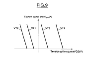
- the curve VT1 corresponds to a threshold voltage of a PMOS transistor of a manufacturing output cell.
- the threshold voltage is of the order of -0.6 volts.
- the erasure of this programmed cell aims to reduce the threshold voltage of the transistor substantially to its initial value (curve VT1).
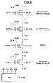
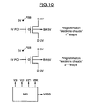
- the biasing means MPL will program a memory cell that has been erased and whose transistor is a PMOS transistor, causing a hot electron programming at the transistor in two successive steps, so as to first compensate any residual positive charges present in the floating gate and then perform an optimal programming ( figure 10 ).
- the polarization means MPL compensates for any residual positive charges present in the floating gate by applying a compensation voltage VZ1 to the contact PC1 of the first active zone.
- This voltage VZ1 is for example equal to 0 volts, but it could also be negative, for example greater than -500 mV approximately. However, care should be taken not to apply a too negative compensation voltage in order not to put in direct conduction the PN diode formed by the box RG1 and the box RG3.
- this compensation voltage for example for 500 microseconds, not only makes it possible to compensate for the negative offset of the threshold voltage, but also to initiate programming by hot electrons.
- the threshold voltage is shifted to the right with respect to the initial voltage (VT3 curve shifted to the right with respect to the VT1 curve).
- Optimum programming is done by then applying, for example for 100 microseconds, a voltage VZ1 on the contact PC1 equal to 5 volts. The threshold voltage is then again shifted to the right (curve VT4).
- this variant of the invention makes it possible to overcome the disadvantage associated with over-erasure by employing two-step programming using the contact PC1 which is usually used for erasure.
- the contact PC1, doped N + 'of the first active zone may extend over the entire surface of this first active zone, except of course under the first portion P1 of the gate material
- a PIN diode is formed in the gate material, ie a diode formed a P + region, and an N + region separated by an intrinsic gate material region.
- this diode is polarized in reverse and can somewhat counteract the erasure efficiency. This is the reason why, in some applications, it will be preferred to use the embodiment illustrated on the figures 1 , la and 1b.
- the PC1 handshake can remain localized and the rest of the N-doped RO1 active area.
- FIG. 3a and 3b Another conceivable embodiment is that illustrated on the Figures 3, 3a and 3b .
- the absence of STI isolation zones between the first active zone and the second active zone is noted on the surface. Insulation is performed here only by reverse biased PN junctions.
- the first active zone is implanted at the surface of the N + type.
- the N + contact could be localized and one could also have a P + implantation of the type surface area similar to that illustrated on the figures 1 .
- This embodiment in which the layer of gate material extends fully above the active areas of the memory cell without overlapping side isolation region, allows for better data retention. Indeed, this avoids the phenomenon of oxide thinning at the interface between an insulation zone and the gate material.
- the embodiment of the cell illustrated on the figure 5 will make it possible to realize a memory plan such as that illustrated on the figure 6 , offering a reduced architecture with a strong cell programming current and good isolation between bit lines.
- a memory cell CEL i that is supposed here to be framed by two adjacent memory cells CEL i-1 and CEL i + 1 located in a same column CL j that said memory cell ( figure 6 ), comprises an access transistor referenced TACS i .
- This access transistor TACS i assigned to the memory cell CEL i , partially surrounds the floating gate transistor FG of the memory cell.
- this access transistor TACS i can be decomposed into three elementary access transistors.
- a first elementary access transistor TACSEL1 i is specifically associated with the memory cell CEL i .
- the second elementary access transistor TACSEL2 i and the third elementary access transistor TACSEL3 i are respectively common to the two access transistors TACS i-1 and TACS i + 1 assigned respectively to the two adjacent memory cells CEL i -1 and CEL i-1.
- the source of the access transistor TACS i forms the source of the first elementary access transistor TACSEL1 i .
- the drain of the first elementary access transistor TACSEL1 i forms part of the source S of the floating gate transistor FG of the memory cell.
- each column of memory cell for example column CL j, comprises a layer of MTL gate material j having a main portion PMTL extending in the direction of the column along and opposite the all floating gate transistors FG cells.
- the gate GREL1 i of the first elementary transistor TACSEL1 i of access transistor TACS i then comprises the portion of said main portion of the layer of gate material MTL j located vis-à-vis the floating gate FG of the cell transistor CEL i .
- this layer of gate material MTL j comprises, at the level of each memory cell, for example at the level of the memory cell CEL i , a second elementary portion E2MTL j connected to the main part PMTL j and extending substantially perpendicular to this main portion of one side of the floating gate transistor.
- This second elementary portion E2MTL j then forms a part of the gate GREL2 i of the second elementary transistor TACSEL2 i .
- the layer of gate material MTL j also includes a third elementary portion E3MTL j also connected to the main portion LLMP j and extending substantially perpendicularly to this main part on the other side of the floating gate transistor of the cell CEL i.
- This third elementary portion E3MTL j forms part of the gate GREL3 i of the third elementary transistor TACSEL3 i .
- the second elementary portion E2MTL j associated with a memory cell forms the third elementary portion associated with one of the two adjacent memory cells
- the third elementary portion E3MTL j associated with the memory cell CEL i forms the second portion elementary associated with the other adjacent memory cells.
- each TACS access transistor i comprises a plurality of SLC contacts which are all connected together by means of the same metallization.
- the BLC drain contacts of the memory cells of the same line are connected together and therefore form a bit line.
- the layer of gate material MTL j in each column is also intended to be biased by a gate voltage bias, and the metallization intended to convey the gate bias voltage on the MTL layer j forms a column metallization ( " row line ").
- the memory device comprises biasing means MPL2 capable of selecting at least one memory cell in programming and reading, and able to erase the memory plane in blocks of cells, in the species here by two columns simultaneously.
- the biasing means are therefore able to apply the same source biasing voltage to the respective SLC sources of the access transistors assigned respectively to the memory cells of the same column.
- these polarization means MPL2 can apply a same gate bias voltage to the respective gates of the access transistors assigned respectively to the memory cells of the same column.
- the biasing means may apply the same erase voltage to the first respective active areas RG1 of the memory cells of at least one and in particular two adjacent columns.
- the biasing means MPL2 have a programming state in which they are able to program a memory cell. They also have a read state in which they are able to read a memory cell. And they have an erase state in which they are able to erase at least one column of memory cells.
- the biasing means are able to apply predetermined voltages to the sources and gates of the access transistors, as well as to the drains and substrates of the floating gate transistors of the cells, as well as to the first ones. active areas RG1.
- the biasing means MPL2 passes the access transistors of the memory cells belonging to the same column as that of the memory cell in question.
- the polarization means apply an identical voltage on the source of the access transistor and the drain of the floating gate transistor of each memory cell of said column, different from the memory cell considered, so that the other memory cells in the column are not requested.
- biasing means MPL2 block the access transistors of the memory cells belonging to another column than that of the memory cell in question.
- the biasing means MPL2 then apply a voltage VBL equal to 0 volts on the contact BLC (bit line) and they apply voltages VBK, VPSB and VZ1 respectively equal to 5 volts, 0 volts and 5 volts respectively on the contacts BK, PSB and PC1.
- the cell is then programmed by hot electrons.
- the invention is remarkable in that since the MTL gate material layer j forms an equipotential, all the access transistors, i.e. Basic accesses are on the go, and help to provide the programming current to the cell in question. Of course, the majority contribution is provided by the access transistor of the cell and the contribution of an access transistor is even lower than this access transistor is remote from the memory cell that is accessed .
- the biasing means MPL2 apply on the gates of the transistors access MTL n a voltage VMTL equal to the voltage VSLC. Thus, all the access transistors of the cells of these other columns are blocked since the gate / source voltage difference is zero.
- the polarization means MPL2 apply a voltage equal to 0 volts on the gates of the access transistors and a voltage equal to 3.3 volts on the sources of the transistors d. access, so as to make the access transistors of the cells of the pass-through column.
- the drain-source voltage difference of the floating gate transistor is voluntarily limited to -1 volts so as to avoid very slow reprogramming of the memory cell.
- the BK substrate will be polarized at 3.3 volts. For example, the ground on the PSB contact point and 3.3 volts on the PC1 contact point will be applied.
- the polarization means cause a Fowler-Nordheim type erasure by applying a voltage on the first active areas RG1 much higher than that applied on the source regions of the access transistors and on the drain and substrate regions of the floating gate transistors.
- the biasing means MPL2 may apply a voltage VZ1 on the contact PC1 equal to 11 volts while the mass will be applied to all other contacts.
- the source of the floating gate transistor of the memory cell is itself floating, is compatible with a deletion Fowler-Nordheim type via the first active area RG1. Indeed, the floating source of the transistor is pulled to the ground by the memory point itself.
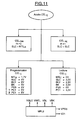
- two-step hot electron cell programming can also apply to the memory map of the figure 6 . More specifically, as illustrated on the figure 11 , the biasing means MPL2 would then apply in this case for the programming of the CEL cell ij , first a zero voltage VZ1 on the contact PC1 via the metallization MTLPC i, j + 1 ( figure 6 ), then an optimal voltage VZ1 of 5 volts.
- the access transistor TACS i assigned to a memory cell CEL ij comprises a GRTACS gate i extending perpendicular to said connecting portion PL and opposite this connecting portion relative to the annular gate FG.
- the source of the access transistor has a source contact BL j .
- the drain of the access transistor forms part of the source S of the floating gate transistor of the memory cell.
- the drain of the floating gate transistor is electrically connected to the second active zone RG2, that is to say to its substrate (bulk).
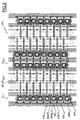
- the drain zone comprises a contact WLP i connected by a metallization, not shown on the figure 12 but schematically illustrated on the figure 13 in contact with substrate BK i .
- All the first active areas of the cells of the same column j of the memory plane are connected together by their contact PC1 j and via another metallization VERJ column.
- the grids GRTACS i access transistors of the cells of the same line i of the memory plane are connected together, and the coorespondants contacts WL i are also connected together by a line metallization WLi.
- the memory device further comprises bias means MPL3 ( figure 15 ) able to select at least one memory cell in programming and to program it by programming of the Fowler-Nordheim type.
- the polarization means are able to select a cell of the memory plane and to program it by applying a sufficient potential difference between the drain of the floating gate transistor of the cell and the first active zone of the cell. this cell.
- FIG. figure 15 An example of voltages delivered by the polarization means MPL3 and applied to the different metallizations of the memory plane is illustrated on FIG. figure 15 in connection with the figure 13 .
- the configuration 1 of the table represented in the upper part of the figure 15 corresponds to a selection and a programming of cell CEL 11 of the figure 13 .
- the supply voltage VPP of the integrated circuit is equal to 6.6 volts, since the oxide thickness of the transistors of the cells is of the order of 5 nanometers.
- This VPP voltage is applied to the metallizations WL1 and WLP1, whereas the voltage VPP / 2 is applied to the metallizations BL1, BL2, WLP2 and VER2.
- the cell Since there is then a large potential difference (typically 5.6 volts) between the floating gate and the contact PC1 1 , the cell is programmed by Fowler-Nordheim type programming.
- the polarization means MPL3 are moreover able to erase the memory plane in its entirety, for example by applying a high voltage to all the first active areas of all the cells, and by applying a zero voltage to the other contacts of the cells.
- the polarization means MPL3 are also able to read the line memory plane by passing the access transistors of the cells of one line and blocking the access transistors of the cells of the other lines.
- the biasing means MPL3 deliver a zero VPSB voltage on the substrate contact PSB.
Landscapes
- Non-Volatile Memory (AREA)
- Semiconductor Memories (AREA)
Claims (33)
- Halbleiterspeichervorrichtung, mit einer elektrisch löschbaren und programmierbaren nichtflüchtigen Speicherzelle mit einer einzigen Gate-Materialschicht und mit einem Transistor mit schwebendem Gate sowie mit einem Steuergate, dadurch gekennzeichnet, dass der Source-Bereich (S), der Drain-Bereich (D) und der Kanal des Transistors mit schwebendem Gate das Steuergate bilden und dass die Speicherzelle eine dielektrische Zone (ZTN) enthält, die zwischen einem ersten Teil (P1) der Gate-Materialschicht und einer ersten aktiven Halbleiterzone (RG1), die von einer das Steuergate enthaltenden zweiten aktiven Zone (RG2) elektrisch isoliert ist, angeordnet ist, wobei diese dielektrische Zone eine Tunnelzone (ZTN) bildet, um bei einer Löschung der Zelle in dem schwebenden Gate gespeicherte Ladungen zu der ersten aktiven Zone zu transportieren.
- Vorrichtung nach Anspruch 1, dadurch gekennzeichnet, dass der kapazitive Wert der Tunnelzone (ZTN) kleiner oder gleich 30 % des gesamten kapazitiven Werts zwischen der Gate-Materialschicht und der Gesamtheit der aktiven Zonen der Speicherzelle ist.
- Vorrichtung nach Anspruch 1 oder 2, dadurch gekennzeichnet, dass der Transistor ein ringförmiges Gate (FG) besitzt und dass die Gate-Materialschicht außer dem ringförmigen Gate (FG) und dem ersten Teil (P1) einen Verbindungsteil (PL) zwischen diesem ersten Teil und dem ringförmigen Gate aufweist.
- Vorrichtung nach einem der vorhergehenden Ansprüche, dadurch gekennzeichnet, dass die erste aktive Zone (RG1) und die zweite aktive Zone (RG2) voneinander durch PN-Übergänge, die dazu vorgesehen sind, entgegengesetzt vorgespannt zu werden, elektrisch isoliert sind.
- Vorrichtung nach Anspruch 4, dadurch gekennzeichnet, dass die erste aktive Zone (RG1) und die zweite aktive Zone (RG2) relativ zueinander an der Oberfläche durch einen Isolationsbereich (STI) elektrisch isoliert sind.
- Vorrichtung nach Anspruch 5, dadurch gekennzeichnet, dass die erste aktive Zone in einem ersten Substratbereich (RG1) verwirklicht ist, der von einem ersten Leitfähigkeitstyp ist, dass die zweite aktive Zone in einem zweiten Substratbereich (RG2) verwirklicht ist, der ebenfalls von dem ersten Leitfähigkeitstyp ist, dass der erste Substratbereich und der zweite Substratbereich durch einen dritten Substratbereich (RG3) getrennt sind, der von einem von dem ersten Leitfähigkeitstyp verschiedenen zweiten Leitfähigkeitstyp ist, und dass sich der Isolationsbereich zwischen dem ersten Substratbereich und dem zweiten Substratbereich erstreckt und eine Öffnung aufweist, die in eine Kontaktherstellungszone (PSB) des dritten Halbleiterbereichs mündet.
- Vorrichtung nach Anspruch 4, dadurch gekennzeichnet, dass die erste aktive Zone in einem ersten Substratbereich (RG1) verwirklicht ist, der von einem ersten Leitfähigkeitstyp ist, dass die zweite aktive Zone in einem zweiten Substratbereich verwirklicht ist, der ebenfalls von dem ersten Leitfähigkeitstyp ist, dass der erste Substratbereich und der zweite Substratbereich durch einen dritten Substratbereich (RG3) getrennt sind, der von einem von dem ersten Leitfähigkeitstyp verschiedenen zweiten Leitfähigkeitstyp ist, und dass sich die Gate-Materialschicht (FG, P1, P2) einteilig über die drei Substratbereiche erstreckt, ohne mit dem Isolationsbereich (STI) zu überlappen.
- Vorrichtung nach Anspruch 6 oder 7, dadurch gekennzeichnet, dass der erste Substratbereich (RG1) an der Oberfläche eine Kontaktherstellungszone (PC1) aufweist, die vom ersten Leitfähigkeitstyp ist.
- Vorrichtung nach Anspruch 8, dadurch gekennzeichnet, dass der erste Substratbereich (RG1) außerdem eine Oberflächenzone (ZS) aufweist, die vom zweiten Leitfähigkeitstyp ist und sich um die Tunnelzone erstreckt, wobei diese Oberflächenzone (ZS) mit der Kontaktherstellungszone (PC1) elektrisch verbunden ist.
- Vorrichtung nach einem der vorhergehenden Ansprüche, dadurch gekennzeichnet, dass der Transistor ein PMOS-Transistor ist.
- Vorrichtung nach einem der vorhergehenden Ansprüche, dadurch gekennzeichnet, dass sie eine Speicherebene enthält, die mehrere Speicherzellen besitzt, wobei jeder Speicherzelle ein Zugriffstransistor zugewiesen ist.
- Vorrichtung nach einem der vorhergehenden Ansprüche, dadurch gekennzeichnet, dass sie außerdem Vorspannungsmittel (MPL) enthält, die einen Zustand zum Programmieren der Speicherzelle, einen Zustand zum Lesen der Speicherzelle und einen Zustand zum Löschen der Speicherzelle besitzen, dass in jedem der Zustände die Vorspannungsmittel an die Source, den Drain und das Substrat des Transistors und an die erste aktive Zone vorgegebene Spannungen anlegen können und dass im Löschzustand die Vorspannungsmittel eine Löschung des Fowler-Nordheim-Typs hervorrufen, indem sie an die erste aktive Zone eine Spannung anlegen, die viel höher als jene ist, die an die Bereiche der Source, des Drains und des Substrats des Transistors angelegt werden.
- Vorrichtung nach Anspruch 12, dadurch gekennzeichnet, dass im Löschzustand die Vorspannungsmittel (MPL) an die Bereiche der Source, des Drains und des Substrats des Transistors gleiche Spannungen anlegen.
- Vorrichtung nach einem der Ansprüche 12 oder 13, dadurch gekennzeichnet, dass im Programmierzustand die Vorspannungsmittel (MPL) eine Programmierung durch heiße Träger auf Seiten des Transistors hervorrufen.
- Vorrichtung nach einem der Ansprüche 12 oder 13, dadurch gekennzeichnet, dass im Programmierzustand die Vorspannungsmittel (MPL) eine Programmierung des Fowler-Nordheim-Typs hervorrufen, indem sie an die Bereiche der Source, des Drains und des Substrats des Transistors gleiche Spannungen anlegen, die viel höher als jene sind, die an die erste aktive Zone angelegt wird.
- Vorrichtung nach einem der Ansprüche 12 bis 15, dadurch gekennzeichnet, dass im Lesezustand der Unterschied zwischen der Drain-/Source-Spannung auf einen Absolutwert von 1 Volt begrenzt ist.
- Vorrichtung nach Anspruch 11, dadurch gekennzeichnet, dass der Zugriffstransistor (TACSi), der einer Speicherzelle zugewiesen ist, die von zwei benachbarten Speicherzellen eingerahmt ist, die sich in derselben Spalte wie die betrachtete Speicherzelle befinden, einen ersten elementaren Zugriffstransistor (TACSEL1i), der speziell dieser Speicherzelle zugeordnet ist, und einen zweiten elementaren Zugriffstransistor (TACSEL2i) sowie einen dritten elementaren Zugriffstransistor (TACSEL3i), die den zwei Zugriffstransistoren gemeinsam sind, die den zwei entsprechenden benachbarten Speicherzellen zugewiesen sind, enthält, dass die Source (SLC) des Zugriffstransistors (TACSi) die Source des ersten elementaren Zugriffstransistors bildet, während der Drain des ersten elementaren Zugriffstransistors einen Teil der Source des Transistors mit schwebendem Gate der Speicherzelle bildet, und dass die Vorrichtung außerdem Vorspannungsmittel (MPL2) enthält, die wenigstens eine Speicherzelle zur Programmierung und zum Lesen auswählen können und die Speicherebene zellenblockweise löschen können.
- Vorrichtung nach Anspruch 17, dadurch gekennzeichnet, dass die Vorspannungsmittel (MPL2) dieselbe Source-Vorspannung an die jeweiligen Sources der Zugriffstransistoren anlegen können, die den jeweiligen Speicherzellen derselben Spalte zugewiesen sind, dieselbe Gate-Vorspannung an die jeweiligen Gates der Zugriffstransistoren anlegen können, die den jeweiligen Speicherzellen derselben Spalte zugewiesen sind, und dieselbe Löschspannung an die ersten aktiven Zonen der Speicherzellen wenigstens einer Spalte anlegen können.
- Vorrichtung nach Anspruch 17 oder 18, dadurch gekennzeichnet, dass der Zugriffstransistor (TACSi), der einer Speicherzelle zugewiesen ist, den Transistor mit schwebendem Gate dieser Speicherzelle teilweise umgibt.
- Vorrichtung nach Anspruch 19, dadurch gekennzeichnet, dass jede Spalte (CLj) von Speicherzellen eine Gate-Materialschicht (MTLj) aufweist, die einen Hauptteil (PMTLj) besitzt, der sich in Richtung der Spalte längs der und gegenüber den Transistoren mit schwebendem Gate der Zellen erstreckt, dass das Gate des ersten elementaren Transistors eines Zugriffstransistors, der einer Speicherzelle zugewiesen ist, den Abschnitt des Hauptteils der Gate-Materialschicht aufweist, der sich gegenüber dem Transistor mit schwebendem Gate dieser Zelle befindet, dass eine Gate-Materialschicht auf Seiten jeder Speicherzelle einen zweiten elementaren Abschnitt (E2MTLj) enthält, der mit dem Hauptteil verbunden ist und sich im Wesentlichen senkrecht zu diesem Hauptteil auf einer Seite des Transistors mit schwebendem Gate der Zelle erstreckt, derart, dass ein Teil des Gates des zweiten elementaren Transistors des Zugriffstransistors gebildet wird, sowie einen dritten elementaren Abschnitt (E3MTLj) enthält, der mit dem Hauptteil verbunden ist und sich im Wesentlichen senkrecht zu diesem Hauptteil auf der anderen Seite des Transistors mit schwebendem Gate der Zelle erstreckt, derart, dass ein Teil des Gates des dritten elementaren Transistors des Zugriffstransistors gebildet wird, und dass der zweite elementare Abschnitt, der einer Speicherzelle zugeordnet ist, den dritten elementaren Abschnitt bildet, der einer der zwei benachbarten Speicherzellen zugeordnet ist, während der dritte elementare Abschnitt, der der Speicherzelle zugeordnet ist, den zweiten elementaren Abschnitt bildet, der der anderen der zwei benachbarten Speicherzellen zugeordnet ist.
- Vorrichtung nach einem der Ansprüche 17 bis 20, dadurch gekennzeichnet, dass die Vorspannungsmittel (MPL2) einen Programmierzustand besitzen, in dem sie eine Speicherzelle programmieren können, einen Lesezustand besitzen, in dem sie eine Speicherzelle lesen können, und einen Löschzustand besitzen, in dem sie wenigstens eine Spalte von Speicherzellen löschen können, dass in jedem der Zustände die Vorspannungsmittel vorgegebene Spannungen an die Sources und die Gates der Zugriffstransistoren sowie an die Drains und die Substrate der Transistoren mit schwebenden Gates der Zellen und an die ersten aktiven Zonen anlegen können und dass im Löschzustand die Vorspannungsmittel eine Löschung des Fowler-Nordheim-Typs hervorrufen, indem sie an die ersten aktiven Zonen eine Spannung anlegen, die viel höher ist als jene, die an die Source-Bereiche der Zugriffstransistoren und an die Drain- und SubstratBereiche der Transistoren mit schwebendem Gate angelegt werden.
- Vorrichtung nach Anspruch 21, dadurch gekennzeichnet, dass die Vorspannungsmittel (MPL2), um auf eine Speicherzelle zum Lesen oder zum Programmieren zuzugreifen, die Zugriffstransistoren der Speicherzellen, die zur selben Spalte wie jene der betrachteten Speicherzelle gehören, durchschalten, an die Source des Zugriffstransistors und an den Drain des Transistors mit schwebendem Gate jeder Speicherzelle der Spalte, die von der betrachteten Speicherzelle verschieden ist, dieselbe Spannung anlegen und die Zugriffstransistoren der Speicherzellen, die zu einer anderen Spalte als jener der betrachteten Speicherzelle gehören, sperren.
- Vorrichtung nach Anspruch 14 oder nach einem der Ansprüche 21 oder 22, dadurch gekennzeichnet, dass die Vorspannungsmittel (MPL; MPL2) eine Speicherzelle programmieren können, die einer Löschung unterworfen worden ist und deren Transistor ein PMOS-Transistor ist, indem sie eine Programmierung durch heiße Elektronen auf Seiten des Transistors in zwei aufeinander folgenden Schritten (PC1 = 0 V; PC1 = 5 V) hervorrufen, derart, dass zunächst die eventuellen positiven Restladungen, die in dem schwebenden Gate vorhanden sind, kompensiert werden und dann eine optimale Programmierung ausgeführt wird.
- Vorrichtung nach Anspruch 23, dadurch gekennzeichnet, dass im ersten Schritt die Vorspannungsmittel (MPL1; MPL2) die eventuellen positiven Restladungen, die in dem schwebenden Gate vorhanden sind, kompensieren, indem sie an den Kontakt (PC1) der ersten aktiven Zone eine Kompensationsspannung (VZ1) anlegen.
- Vorrichtung nach Anspruch 24, dadurch gekennzeichnet, dass die Kompensationsspannung (VZ1) kleiner oder gleich 0 Volt und größer als etwa -500 mV ist.
- Vorrichtung nach den Ansprüchen 3 bis 11, dadurch gekennzeichnet, dass der einer Speicherzelle zugewiesene Zugriffstransistor (TACSi) ein Gate (GRTACSi) aufweist, das sich senkrecht zu dem Verbindungsteil (PL) und gegenüber diesem Verbindungsteil in Bezug auf das ringförmige Gate erstreckt, dass die Source des Zugriffstransistors einen Source-Kontakt (BLj) aufweist, dass der Drain des Zugriffstransistors einen Teil der Source des Transistors mit schwebendem Gate der Speicherzelle bildet und dass der Drain des Transistors mit schwebendem Gate mit der zweiten aktiven Zone (RG2) elektrisch verbunden ist.
- Vorrichtung nach Anspruch 26, dadurch gekennzeichnet, dass alle Source-Kontakte der Zugriffstransistoren der Zellen derselben Spalte der Speicherebene miteinander verbunden sind (BL1), dass alle aktiven ersten Zonen der Zellen derselben Spalte der Speicherebene miteinander verbunden sind (VER1), dass die Gates der Zugriffstransistoren der Zellen derselben Zeile der Speicherebene miteinander verbunden sind und dass die entsprechenden Gate-Kontakte (WLi) durch eine Zeilenmetallisierung (WL1) miteinander verbunden sind, dass die Drains der Transistoren mit schwebenden Gates der Zellen derselben Zeile der Speicherebene miteinander verbunden sind, um eine andere Zeilenmetallisierung (WLP1) zu bilden, und dass die Vorrichtung außerdem Vorspannungsmittel (MPL3) enthält, die wenigstens eine Speicherzelle zur Programmierung auswählen können und sie durch eine Programmierung des Fowler-Nordheim-Typs programmieren können.
- Vorrichtung nach Anspruch 27, dadurch gekennzeichnet, dass die Vorspannungsmittel (MPL3) eine Zelle der Speicherebene auswählen können und sie durch Anlegen einer ausreichenden Potentialdifferenz zwischen dem Drain des Transistors mit schwebendem Gate der Zelle und der ersten aktiven Zone dieser Zelle programmieren können.
- Vorrichtung nach Anspruch 27 oder 28, dadurch gekennzeichnet, dass die Vorspannungsmittel (MPL3) die Speicherebene als Ganzes löschen können.
- Vorrichtung nach Anspruch 29, dadurch gekennzeichnet, dass die Vorspannungsmittel (MPL3) die Speicherebene als Ganzes löschen können, indem sie an alle ersten aktiven Zonen aller Zellen eine hohe Spannung anlegen und indem sie an die anderen Kontakte der Zellen eine Nullspannung anlegen.
- Vorrichtung nach einem der Ansprüche 27 bis 30, dadurch gekennzeichnet, dass die Vorspannungsmittel (MPL3) die Speicherebene zeilenweise lesen können, indem sie die Zugriffstransistoren der Zellen einer Zeile durchschalten und indem sie die Zugriffstransistoren der Zellen der anderen Zeilen sperren.
- Vorrichtung nach einem der vorhergehenden Ansprüche, dadurch gekennzeichnet, dass sie einen Speicher des EEPROM-Typs oder des FLASH-Typs bildet.
- Integrierte Schaltung, dadurch gekennzeichnet, dass sie eine Vorrichtung nach einem der Ansprüche 1 bis 32 enthält.
Applications Claiming Priority (5)
| Application Number | Priority Date | Filing Date | Title |
|---|---|---|---|
| FR0204690A FR2838563B1 (fr) | 2002-04-15 | 2002-04-15 | Dispositif semiconducteur de memoire, non volatile, programmable et effacable electriquement, a une seule couche de materiau de grille |
| FR0204690 | 2002-04-15 | ||
| FR0209454A FR2838554B1 (fr) | 2002-04-15 | 2002-07-25 | Dispositif semiconducteur de memoire, non volatile, programmable et effacable electriquement, a une seule couche de materiau de grille, et plan memoire correspondant |
| FR0209454 | 2002-07-25 | ||
| PCT/FR2003/000311 WO2003088366A1 (fr) | 2002-04-15 | 2003-01-31 | Dispositif semiconducteur de memoire, non volatile, programmable et effacable electriquement, a une seule couche de materiau de grille, et plan memoire correspondant |
Publications (2)
| Publication Number | Publication Date |
|---|---|
| EP1495496A1 EP1495496A1 (de) | 2005-01-12 |
| EP1495496B1 true EP1495496B1 (de) | 2009-11-18 |
Family
ID=28676465
Family Applications (1)
| Application Number | Title | Priority Date | Filing Date |
|---|---|---|---|
| EP03709915A Expired - Lifetime EP1495496B1 (de) | 2002-04-15 | 2003-01-31 | Elektrisch löschbare und programmiebare nichtflüchtige halbleiterspeicheranordnung mit einschichtigem gatematerial und entsprechende speicherfläche |
Country Status (7)
| Country | Link |
|---|---|
| US (1) | US7333362B2 (de) |
| EP (1) | EP1495496B1 (de) |
| JP (1) | JP4662529B2 (de) |
| AT (1) | ATE449424T1 (de) |
| DE (1) | DE60330130D1 (de) |
| FR (1) | FR2838554B1 (de) |
| WO (1) | WO2003088366A1 (de) |
Families Citing this family (31)
| Publication number | Priority date | Publication date | Assignee | Title |
|---|---|---|---|---|
| TWI231039B (en) * | 2004-04-30 | 2005-04-11 | Yield Microelectronics Corp | Non-volatile memory and its operational method |
| GB0415995D0 (en) | 2004-07-16 | 2004-08-18 | Song Aimin | Memory array |
| JP4881552B2 (ja) * | 2004-09-09 | 2012-02-22 | ルネサスエレクトロニクス株式会社 | 半導体装置 |
| JP2006202834A (ja) * | 2005-01-18 | 2006-08-03 | Seiko Epson Corp | 半導体記憶装置および半導体記憶装置の製造方法 |
| US7402874B2 (en) * | 2005-04-29 | 2008-07-22 | Texas Instruments Incorporated | One time programmable EPROM fabrication in STI CMOS technology |
| JP2006344735A (ja) * | 2005-06-08 | 2006-12-21 | Seiko Epson Corp | 半導体装置 |
| FR2891398A1 (fr) * | 2005-09-23 | 2007-03-30 | St Microelectronics Sa | Memoire non volatile reprogrammable |
| JP2007149947A (ja) * | 2005-11-28 | 2007-06-14 | Nec Electronics Corp | 不揮発性メモリセル及びeeprom |
| JP4435095B2 (ja) * | 2006-01-04 | 2010-03-17 | 株式会社東芝 | 半導体システム |
| US20070247915A1 (en) * | 2006-04-21 | 2007-10-25 | Intersil Americas Inc. | Multiple time programmable (MTP) PMOS floating gate-based non-volatile memory device for a general-purpose CMOS technology with thick gate oxide |
| CN100508169C (zh) * | 2006-08-02 | 2009-07-01 | 联华电子股份有限公司 | 单层多晶硅可电除可程序只读存储单元的制造方法 |
| US7759727B2 (en) | 2006-08-21 | 2010-07-20 | Intersil Americas Inc. | Method and apparatus for shielding tunneling circuit and floating gate for integration of a floating gate voltage reference in a general purpose CMOS technology |
| JP4282705B2 (ja) * | 2006-09-28 | 2009-06-24 | 株式会社東芝 | エージングデバイス及びその製造方法 |
| ES2322418B1 (es) * | 2006-10-02 | 2010-03-22 | Universidad De Almeria | Sistema de coexpresion enzimatica para la produccion de d-aminoacidos. |
| US7663173B1 (en) * | 2007-01-12 | 2010-02-16 | National Semiconductor Corporation | Non-volatile memory cell with poly filled trench as control gate and fully isolated substrate as charge storage |
| US7808034B1 (en) * | 2007-01-12 | 2010-10-05 | National Semiconductor Corporation | Non-volatile memory cell with fully isolated substrate as charge storage |
| US7688627B2 (en) * | 2007-04-24 | 2010-03-30 | Intersil Americas Inc. | Flash memory array of floating gate-based non-volatile memory cells |
| US7903465B2 (en) * | 2007-04-24 | 2011-03-08 | Intersil Americas Inc. | Memory array of floating gate-based non-volatile memory cells |
| US8339862B2 (en) | 2007-12-25 | 2012-12-25 | Genusion, Inc. | Nonvolatile semiconductor memory device |
| WO2009123203A1 (ja) * | 2008-04-02 | 2009-10-08 | シャープ株式会社 | 不揮発性半導体記憶装置 |
| TWI416713B (zh) * | 2008-09-30 | 2013-11-21 | 國立大學法人九州工業大學 | Floating Gate Type Nonvolatile Memory Configuration |
| US7983081B2 (en) * | 2008-12-14 | 2011-07-19 | Chip.Memory Technology, Inc. | Non-volatile memory apparatus and method with deep N-well |
| US9324866B2 (en) | 2012-01-23 | 2016-04-26 | Taiwan Semiconductor Manufacturing Company, Ltd. | Structure and method for transistor with line end extension |
| JP5856836B2 (ja) * | 2011-12-16 | 2016-02-10 | セイコーインスツル株式会社 | 不揮発性半導体記憶装置 |
| US10573751B2 (en) | 2012-01-23 | 2020-02-25 | Taiwan Semiconductor Manufacturing Company, Ltd. | Structure and method for providing line end extensions for fin-type active regions |
| JP2013187534A (ja) * | 2012-03-08 | 2013-09-19 | Ememory Technology Inc | 消去可能プログラマブル単一ポリ不揮発性メモリ |
| EP2639817A1 (de) * | 2012-03-12 | 2013-09-18 | eMemory Technology Inc. | Verfahren zum Herstellen einer Floating-gate-Speichervorrichtung mit einer einzelnen Polysiliziumschicht |
| CN102723333B (zh) * | 2012-07-11 | 2014-09-03 | 无锡来燕微电子有限公司 | 一种具有p+浮栅电极的非挥发性记忆体及其制备方法 |
| KR102166525B1 (ko) * | 2014-04-18 | 2020-10-15 | 에스케이하이닉스 주식회사 | 단일층의 게이트를 갖는 불휘발성 메모리소자 및 그 동작방법과, 이를 이용한 메모리 셀어레이 |
| CN108257963A (zh) * | 2016-12-29 | 2018-07-06 | 北京同方微电子有限公司 | 一种闪存存储单元 |
| US12051756B2 (en) * | 2021-07-16 | 2024-07-30 | Taiwan Semiconductor Manufacturing Company, Ltd. | Flash memory device and method thereof |
Family Cites Families (17)
| Publication number | Priority date | Publication date | Assignee | Title |
|---|---|---|---|---|
| JP2677327B2 (ja) * | 1988-07-11 | 1997-11-17 | 株式会社日立製作所 | 半導体装置 |
| JPH03179780A (ja) * | 1989-12-07 | 1991-08-05 | Fujitsu Ltd | 半導体装置 |
| US5712180A (en) * | 1992-01-14 | 1998-01-27 | Sundisk Corporation | EEPROM with split gate source side injection |
| JP2596695B2 (ja) * | 1993-05-07 | 1997-04-02 | インターナショナル・ビジネス・マシーンズ・コーポレイション | Eeprom |
| JPH06334194A (ja) * | 1993-05-25 | 1994-12-02 | Fuji Electric Co Ltd | 不揮発性半導体メモリ |
| JPH07183410A (ja) * | 1993-12-24 | 1995-07-21 | Mitsubishi Electric Corp | 不揮発性半導体記憶装置 |
| US5761121A (en) * | 1996-10-31 | 1998-06-02 | Programmable Microelectronics Corporation | PMOS single-poly non-volatile memory structure |
| US5892709A (en) * | 1997-05-09 | 1999-04-06 | Motorola, Inc. | Single level gate nonvolatile memory device and method for accessing the same |
| US6936849B1 (en) * | 1997-07-29 | 2005-08-30 | Micron Technology, Inc. | Silicon carbide gate transistor |
| US6243289B1 (en) * | 1998-04-08 | 2001-06-05 | Micron Technology Inc. | Dual floating gate programmable read only memory cell structure and method for its fabrication and operation |
| EP0975022A1 (de) * | 1998-07-22 | 2000-01-26 | STMicroelectronics S.r.l. | Herstellungsverfahren für elektronische Bauelemente mit Festwertspeicherzellen und Niederspannungstransistoren, die selbstjustierte Silizidübergänge aufweisen |
| US6025625A (en) * | 1999-02-25 | 2000-02-15 | Worldwide Semiconductor Manufacturing Corporation | Single-poly EEPROM cell structure operations and array architecture |
| KR100665413B1 (ko) * | 1999-03-31 | 2007-01-04 | 코닌클리즈케 필립스 일렉트로닉스 엔.브이. | 반도체 디바이스 |
| US6559007B1 (en) * | 2000-04-06 | 2003-05-06 | Micron Technology, Inc. | Method for forming flash memory device having a tunnel dielectric comprising nitrided oxide |
| EP1402536B1 (de) * | 2001-07-02 | 2006-06-14 | Infineon Technologies AG | Ladungsgekoppelte eeprom anordnung und dazugehöriges betriebsverfahren |
| US6700154B1 (en) * | 2002-09-20 | 2004-03-02 | Lattice Semiconductor Corporation | EEPROM cell with trench coupling capacitor |
| JP4390480B2 (ja) * | 2003-06-04 | 2009-12-24 | パナソニック株式会社 | 不揮発性半導体記憶装置 |
-
2002
- 2002-07-25 FR FR0209454A patent/FR2838554B1/fr not_active Expired - Fee Related
-
2003
- 2003-01-31 EP EP03709915A patent/EP1495496B1/de not_active Expired - Lifetime
- 2003-01-31 AT AT03709915T patent/ATE449424T1/de not_active IP Right Cessation
- 2003-01-31 US US10/511,712 patent/US7333362B2/en not_active Expired - Lifetime
- 2003-01-31 DE DE60330130T patent/DE60330130D1/de not_active Expired - Lifetime
- 2003-01-31 WO PCT/FR2003/000311 patent/WO2003088366A1/fr not_active Ceased
- 2003-01-31 JP JP2003585189A patent/JP4662529B2/ja not_active Expired - Lifetime
Also Published As
| Publication number | Publication date |
|---|---|
| FR2838554B1 (fr) | 2004-07-09 |
| EP1495496A1 (de) | 2005-01-12 |
| JP4662529B2 (ja) | 2011-03-30 |
| US7333362B2 (en) | 2008-02-19 |
| WO2003088366A1 (fr) | 2003-10-23 |
| JP2005522884A (ja) | 2005-07-28 |
| FR2838554A1 (fr) | 2003-10-17 |
| US20050219912A1 (en) | 2005-10-06 |
| ATE449424T1 (de) | 2009-12-15 |
| DE60330130D1 (de) | 2009-12-31 |
Similar Documents
| Publication | Publication Date | Title |
|---|---|---|
| EP1495496B1 (de) | Elektrisch löschbare und programmiebare nichtflüchtige halbleiterspeicheranordnung mit einschichtigem gatematerial und entsprechende speicherfläche | |
| FR2499290A1 (fr) | Dispositif de memoire dense remanent electriquement alterable avec electrode de couplage dans le substrat | |
| FR2692720A1 (fr) | Dispositif d'EPROM à couche unique de silicium polycristallin à effacement rapide. | |
| FR3021804A1 (fr) | Cellule memoire non volatile duale comprenant un transistor d'effacement | |
| EP0648375B1 (de) | Flash-eeprom-speicher mit drei gateelektroden und sein herstellungsverfahren. | |
| FR3021803A1 (fr) | Cellules memoire jumelles accessibles individuellement en lecture | |
| FR3030883A1 (fr) | Cellule memoire a grille de selection verticale formee dans un substrat de type fdsoi | |
| FR2996680A1 (fr) | Memoire non volatile comportant des transistors de selection verticaux | |
| FR2953643A1 (fr) | Cellule memoire flash sur seoi disposant d'une seconde grille de controle enterree sous la couche isolante | |
| FR3071355B1 (fr) | Cellule-memoire eeprom compacte | |
| EP1418625B1 (de) | Verfahren zur Speicherung binäre Daten in eine Speicherzelle einer integrierten Speicherschaltung, entsprechende integrierte Schaltung und Verfahren zur Herstellung | |
| EP0896370B1 (de) | Schwebegatterspeicherelement auf SOI und entsprechendes Herstellungsverfahren | |
| FR3080949A1 (fr) | Dispositif de memoire non volatile du type a piegeage de charges et procede de fabrication | |
| EP0354858B1 (de) | Hochintegrierte EPROM-Speicheranordnung mit einem grossen Kopplungsfaktor | |
| FR2955195A1 (fr) | Dispositif de comparaison de donnees dans une memoire adressable par contenu sur seoi | |
| EP0356346B1 (de) | Hochintegrierte EPROM-Speicheranordnung | |
| EP1863035B1 (de) | EEPROM-Speicher mit verbessertem Widerstand gegen Transistordurchbruch | |
| EP1343208A1 (de) | Elektrisch programmierbare und löschbare nichtflüchtige Speicheranordnung mit einem einschichtigen Gatematerial | |
| EP1271657A1 (de) | Integrierte Halbleiterspeicheranordnung des DRAM-Typs und Verfahren zur Herstellung | |
| EP0313427B1 (de) | Speicher in einer integrierten Schaltung | |
| EP3896695A1 (de) | Verfahren zum schreiben in einen nichtflüchtigen speicher in abhängigkeit von der alterung der speicherzellen und entsprechender integrierter schaltkreis | |
| FR2838563A1 (fr) | Dispositif semiconducteur de memoire, non volatile, programmable et effacable electriquement, a une seule couche de materiau de grille | |
| FR3155116A1 (fr) | circuit intégré comportant une cellule mémoire et procédé de fabrication correspondant | |
| EP4485547A1 (de) | Nichtflüchtige speicheranordnung und verfahren zu ihrer herstellung | |
| FR3144402A1 (fr) | Circuit électronique comprenant une cellule de transistors |
Legal Events
| Date | Code | Title | Description |
|---|---|---|---|
| PUAI | Public reference made under article 153(3) epc to a published international application that has entered the european phase |
Free format text: ORIGINAL CODE: 0009012 |
|
| 17P | Request for examination filed |
Effective date: 20040914 |
|
| AK | Designated contracting states |
Kind code of ref document: A1 Designated state(s): AT BE BG CH CY CZ DE DK EE ES FI FR GB GR HU IE IT LI LU MC NL PT SE SI SK TR |
|
| GRAP | Despatch of communication of intention to grant a patent |
Free format text: ORIGINAL CODE: EPIDOSNIGR1 |
|
| GRAS | Grant fee paid |
Free format text: ORIGINAL CODE: EPIDOSNIGR3 |
|
| GRAA | (expected) grant |
Free format text: ORIGINAL CODE: 0009210 |
|
| AK | Designated contracting states |
Kind code of ref document: B1 Designated state(s): AT BE BG CH CY CZ DE DK EE ES FI FR GB GR HU IE IT LI LU MC NL PT SE SI SK TR |
|
| REG | Reference to a national code |
Ref country code: GB Ref legal event code: FG4D Free format text: NOT ENGLISH |
|
| REG | Reference to a national code |
Ref country code: CH Ref legal event code: EP |
|
| REG | Reference to a national code |
Ref country code: IE Ref legal event code: FG4D |
|
| REF | Corresponds to: |
Ref document number: 60330130 Country of ref document: DE Date of ref document: 20091231 Kind code of ref document: P |
|
| REG | Reference to a national code |
Ref country code: NL Ref legal event code: VDEP Effective date: 20091118 |
|
| PG25 | Lapsed in a contracting state [announced via postgrant information from national office to epo] |
Ref country code: SE Free format text: LAPSE BECAUSE OF FAILURE TO SUBMIT A TRANSLATION OF THE DESCRIPTION OR TO PAY THE FEE WITHIN THE PRESCRIBED TIME-LIMIT Effective date: 20091118 Ref country code: FI Free format text: LAPSE BECAUSE OF FAILURE TO SUBMIT A TRANSLATION OF THE DESCRIPTION OR TO PAY THE FEE WITHIN THE PRESCRIBED TIME-LIMIT Effective date: 20091118 Ref country code: PT Free format text: LAPSE BECAUSE OF FAILURE TO SUBMIT A TRANSLATION OF THE DESCRIPTION OR TO PAY THE FEE WITHIN THE PRESCRIBED TIME-LIMIT Effective date: 20100318 Ref country code: ES Free format text: LAPSE BECAUSE OF FAILURE TO SUBMIT A TRANSLATION OF THE DESCRIPTION OR TO PAY THE FEE WITHIN THE PRESCRIBED TIME-LIMIT Effective date: 20100228 |
|
| PG25 | Lapsed in a contracting state [announced via postgrant information from national office to epo] |
Ref country code: SI Free format text: LAPSE BECAUSE OF FAILURE TO SUBMIT A TRANSLATION OF THE DESCRIPTION OR TO PAY THE FEE WITHIN THE PRESCRIBED TIME-LIMIT Effective date: 20091118 Ref country code: CY Free format text: LAPSE BECAUSE OF FAILURE TO SUBMIT A TRANSLATION OF THE DESCRIPTION OR TO PAY THE FEE WITHIN THE PRESCRIBED TIME-LIMIT Effective date: 20091118 |
|
| REG | Reference to a national code |
Ref country code: IE Ref legal event code: FD4D |
|
| PG25 | Lapsed in a contracting state [announced via postgrant information from national office to epo] |
Ref country code: AT Free format text: LAPSE BECAUSE OF FAILURE TO SUBMIT A TRANSLATION OF THE DESCRIPTION OR TO PAY THE FEE WITHIN THE PRESCRIBED TIME-LIMIT Effective date: 20091118 |
|
| PG25 | Lapsed in a contracting state [announced via postgrant information from national office to epo] |
Ref country code: NL Free format text: LAPSE BECAUSE OF FAILURE TO SUBMIT A TRANSLATION OF THE DESCRIPTION OR TO PAY THE FEE WITHIN THE PRESCRIBED TIME-LIMIT Effective date: 20091118 Ref country code: IE Free format text: LAPSE BECAUSE OF FAILURE TO SUBMIT A TRANSLATION OF THE DESCRIPTION OR TO PAY THE FEE WITHIN THE PRESCRIBED TIME-LIMIT Effective date: 20091118 Ref country code: BG Free format text: LAPSE BECAUSE OF FAILURE TO SUBMIT A TRANSLATION OF THE DESCRIPTION OR TO PAY THE FEE WITHIN THE PRESCRIBED TIME-LIMIT Effective date: 20100218 Ref country code: EE Free format text: LAPSE BECAUSE OF FAILURE TO SUBMIT A TRANSLATION OF THE DESCRIPTION OR TO PAY THE FEE WITHIN THE PRESCRIBED TIME-LIMIT Effective date: 20091118 Ref country code: DK Free format text: LAPSE BECAUSE OF FAILURE TO SUBMIT A TRANSLATION OF THE DESCRIPTION OR TO PAY THE FEE WITHIN THE PRESCRIBED TIME-LIMIT Effective date: 20091118 |
|
| BERE | Be: lapsed |
Owner name: STMICROELECTRONICS S.A. Effective date: 20100131 |
|
| PG25 | Lapsed in a contracting state [announced via postgrant information from national office to epo] |
Ref country code: CZ Free format text: LAPSE BECAUSE OF FAILURE TO SUBMIT A TRANSLATION OF THE DESCRIPTION OR TO PAY THE FEE WITHIN THE PRESCRIBED TIME-LIMIT Effective date: 20091118 Ref country code: MC Free format text: LAPSE BECAUSE OF NON-PAYMENT OF DUE FEES Effective date: 20100131 Ref country code: SK Free format text: LAPSE BECAUSE OF FAILURE TO SUBMIT A TRANSLATION OF THE DESCRIPTION OR TO PAY THE FEE WITHIN THE PRESCRIBED TIME-LIMIT Effective date: 20091118 |
|
| REG | Reference to a national code |
Ref country code: CH Ref legal event code: PL |
|
| PLBE | No opposition filed within time limit |
Free format text: ORIGINAL CODE: 0009261 |
|
| STAA | Information on the status of an ep patent application or granted ep patent |
Free format text: STATUS: NO OPPOSITION FILED WITHIN TIME LIMIT |
|
| 26N | No opposition filed |
Effective date: 20100819 |
|
| PG25 | Lapsed in a contracting state [announced via postgrant information from national office to epo] |
Ref country code: GR Free format text: LAPSE BECAUSE OF FAILURE TO SUBMIT A TRANSLATION OF THE DESCRIPTION OR TO PAY THE FEE WITHIN THE PRESCRIBED TIME-LIMIT Effective date: 20100219 Ref country code: CH Free format text: LAPSE BECAUSE OF NON-PAYMENT OF DUE FEES Effective date: 20100131 Ref country code: LI Free format text: LAPSE BECAUSE OF NON-PAYMENT OF DUE FEES Effective date: 20100131 |
|
| PG25 | Lapsed in a contracting state [announced via postgrant information from national office to epo] |
Ref country code: BE Free format text: LAPSE BECAUSE OF NON-PAYMENT OF DUE FEES Effective date: 20100131 |
|
| PGFP | Annual fee paid to national office [announced via postgrant information from national office to epo] |
Ref country code: GB Payment date: 20101230 Year of fee payment: 9 |
|
| PGFP | Annual fee paid to national office [announced via postgrant information from national office to epo] |
Ref country code: IT Payment date: 20101227 Year of fee payment: 9 Ref country code: FR Payment date: 20110216 Year of fee payment: 9 Ref country code: DE Payment date: 20110103 Year of fee payment: 9 |
|
| GBPC | Gb: european patent ceased through non-payment of renewal fee |
Effective date: 20120131 |
|
| PG25 | Lapsed in a contracting state [announced via postgrant information from national office to epo] |
Ref country code: HU Free format text: LAPSE BECAUSE OF FAILURE TO SUBMIT A TRANSLATION OF THE DESCRIPTION OR TO PAY THE FEE WITHIN THE PRESCRIBED TIME-LIMIT Effective date: 20100519 Ref country code: LU Free format text: LAPSE BECAUSE OF NON-PAYMENT OF DUE FEES Effective date: 20100131 |
|
| REG | Reference to a national code |
Ref country code: FR Ref legal event code: ST Effective date: 20120928 |
|
| PG25 | Lapsed in a contracting state [announced via postgrant information from national office to epo] |
Ref country code: TR Free format text: LAPSE BECAUSE OF FAILURE TO SUBMIT A TRANSLATION OF THE DESCRIPTION OR TO PAY THE FEE WITHIN THE PRESCRIBED TIME-LIMIT Effective date: 20091118 Ref country code: GB Free format text: LAPSE BECAUSE OF NON-PAYMENT OF DUE FEES Effective date: 20120131 Ref country code: DE Free format text: LAPSE BECAUSE OF NON-PAYMENT OF DUE FEES Effective date: 20120801 |
|
| REG | Reference to a national code |
Ref country code: DE Ref legal event code: R119 Ref document number: 60330130 Country of ref document: DE Effective date: 20120801 |
|
| PG25 | Lapsed in a contracting state [announced via postgrant information from national office to epo] |
Ref country code: IT Free format text: LAPSE BECAUSE OF NON-PAYMENT OF DUE FEES Effective date: 20120131 |
|
| PG25 | Lapsed in a contracting state [announced via postgrant information from national office to epo] |
Ref country code: FR Free format text: LAPSE BECAUSE OF NON-PAYMENT OF DUE FEES Effective date: 20120131 |