EP0437402A2 - Dispositif de circuit integré semi-conducteur - Google Patents
Dispositif de circuit integré semi-conducteur Download PDFInfo
- Publication number
- EP0437402A2 EP0437402A2 EP91400043A EP91400043A EP0437402A2 EP 0437402 A2 EP0437402 A2 EP 0437402A2 EP 91400043 A EP91400043 A EP 91400043A EP 91400043 A EP91400043 A EP 91400043A EP 0437402 A2 EP0437402 A2 EP 0437402A2
- Authority
- EP
- European Patent Office
- Prior art keywords
- mosfet
- bipolar transistor
- input
- power source
- circuit
- Prior art date
- Legal status (The legal status is an assumption and is not a legal conclusion. Google has not performed a legal analysis and makes no representation as to the accuracy of the status listed.)
- Withdrawn
Links
Images



Classifications
-
- G—PHYSICS
- G11—INFORMATION STORAGE
- G11C—STATIC STORES
- G11C11/00—Digital stores characterised by the use of particular electric or magnetic storage elements; Storage elements therefor
- G11C11/21—Digital stores characterised by the use of particular electric or magnetic storage elements; Storage elements therefor using electric elements
- G11C11/34—Digital stores characterised by the use of particular electric or magnetic storage elements; Storage elements therefor using electric elements using semiconductor devices
- G11C11/40—Digital stores characterised by the use of particular electric or magnetic storage elements; Storage elements therefor using electric elements using semiconductor devices using transistors
- G11C11/401—Digital stores characterised by the use of particular electric or magnetic storage elements; Storage elements therefor using electric elements using semiconductor devices using transistors forming cells needing refreshing or charge regeneration, i.e. dynamic cells
- G11C11/4063—Auxiliary circuits, e.g. for addressing, decoding, driving, writing, sensing or timing
- G11C11/407—Auxiliary circuits, e.g. for addressing, decoding, driving, writing, sensing or timing for memory cells of the field-effect type
-
- H—ELECTRICITY
- H03—ELECTRONIC CIRCUITRY
- H03K—PULSE TECHNIQUE
- H03K3/00—Circuits for generating electric pulses; Monostable, bistable or multistable circuits
- H03K3/02—Generators characterised by the type of circuit or by the means used for producing pulses
- H03K3/353—Generators characterised by the type of circuit or by the means used for producing pulses by the use, as active elements, of field-effect transistors with internal or external positive feedback
- H03K3/356—Bistable circuits
- H03K3/356017—Bistable circuits using additional transistors in the input circuit
Definitions
- the present invention relates to a semiconductor integrated circuit device, and particularly to a semiconductor integrated circuit device used as a differential amplifier circuit for amplifying an output of a sense amplifier, etc.
- IC integrated circuit
- a direct-coupled circuit is frequently used, however, this circuit has a problem of drift.
- a differential amplifier circuit having a pair of transistors is used. The differential amplifier circuit is required to operate at high speed, consume less electric power, and have a large power source and a large temperature margin.
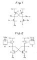
- Figure 1 shows a conventional semiconductor integrated circuit device serving as a differential amplifier circuit. This circuit is interposed between, for example, a sense amplifier of a semiconductor memory and an output buffer circuit, to amplify an output level of the sense amplifier and provide it to the output buffer circuit.
- numerals 1 and 2 denote NMOS transistors for receiving input signals
- 3 and 4 denote PMOS transistors that are cross-connected with the NMOS transistors 1 and 2.
- Nodes 21 and 22 provide output signals.
- Gates of the NMOS transistors 1 and 2 receive binary digital input signals IN1 and IN2, respectively. These input signals are inverted relative to each other.
- Sources of the NMOS transistors 1 and 2 are connected to a ground, i.e., a low-potential power source Vss.
- the input signals IN1 and IN2 form binary levels between, for example, 4 V and 3.1 V.
- the NMOS transistor 1 is turned ON to set the node 21 to Low (L), e.g., 0 V.
- the levels of the input signals IN1 and IN2 are amplified between 0 V and Vcc, and supplied from the nodes 21 and 22 to the outside.
- the input signal IN1 is L, an operation opposite to the above will take place.
- the conventional semiconductor integrated circuit device mentioned above may realize a certain amount of high-speed operation and low power consumption but must be further improved to achieve a speedier operation.
- MOS transistors may be advantageous in reducing power consumption but restrict operation speeds. There is room, therefore, to utilize high-speed characteristics of other active elements such as bipolar transistors.
- An object of the present invention is to provide a level changing semiconductor integrated circuit device serving as a differential amplifier circuit that can operate at high speed and low power consumption.
- the present invention provides a level changing semiconductor integrated circuit comprising a first current path and a second current path.
- the first current path involves a first bipolar transistor and a first MOSFET (Metallic Oxide Semiconductor Field Effect Transistor) that are connected in series.
- the emitter of the first bipolar transistor is connected to one terminal of the first MOSFET, and the collector of the first bipolar transistor is connected to a high-potential power source.
- the other terminal of the first MOSFET is connected to a low-potential power source.
- the second current path involves a second bipolar transistor and a second MOSFET that are connected in series.
- the emitter of the second bipolar transistor is connected to one terminal of the second MOSFET, and the collector of the second bipolar transistor is connected to the high-potential power source.
- the other terminal of the second MOSFET is connected to the low-potential power source.
- the gate of the first MOSFET is cross-connected to the emitter of the second bipolar transistor of the second current path, and the gate of the second MOSFET is cross-connected to the emitter of the first bipolar transistor of the first current path.
- the emitters of the first and second bipolar transistors provide output signals.
- At least two kinds of input signals having different signal levels are simultaneously applied to respective first and second input means of the first and second current paths, thereby controlling currents flowing through the first and second current paths.
- the level changing semiconductor integrated circuit device of the present invention uses a special combination of bipolar transistors and MOSFETs, and controls each output with at least two kinds of input signals having different levels, thereby amplifying the input signals.
- the present invention properly uses characteristics of the bipolar transistors to improve the switching speed of a high-load operation as well as reducing power consumption.
- a level changing semiconductor integrated circuit 40 is disposed between an output of a sense amplifier circuit 41 and a proper output circuit 42 to amplify an output of the sense amplifier circuit 41 and supply the amplified signal to the output circuit 42.
- the level changing circuit 40 has a differential amplifying function.
- the sense amplifier circuit 41 reads data from a memory cell and amplifies the read data.
- the level changing circuit 40 further amplifies the data signal and provides it to the output circuit 42.
- the output circuit 42 buffers and amplifies an output signal of the level changing circuit 40 and provides it to the outside.
- Figure 2 shows a basic arrangement of the level changing semiconductor integrated circuit 40 providing the differential amplifying function.
- the circuit 40 comprises a first current path I1 and a second current path I2.
- the first current path I1 involves a first bipolar transistor 13 and a first MOSFET 15 that are connected in series.
- the emitter of the first bipolar transistor 13 is connected to one terminal of the first MOSFET 15, and the collector of the first bipolar transistor 13 is connected to a high-potential power source Vcc.
- the other terminal of the first MOSFET 15 is connected to a low-potential power source Vss.
- the second current path I2 involves a second bipolar transistor 14 and a second MOSFET 16 that are connected in series.
- the emitter of the second bipolar transistor 14 is connected to one terminal of the second MOSFET 16, and the collector of the second bipolar transistor 14 is connected to the high-potential power source Vcc.
- the other terminal of the second MOSFET transistor 16 is connected to the low-potential power source Vss.
- the gate of the first MOSFET 15 is cross-connected to the emitter of the second bipolar transistor 14 of the second current path I2, and the gate of the second MOSFET 16 is cross-connected to the emitter of the first bipolar transistor 13 of the first current path I1.
- the emitters of the first and second bipolar transistors 13 and 14 provide output signals.
- Two kinds of input signals IN1 and IN2 having different signal levels are simultaneously applied to respective first and second input means 17 and 18 of the first and second current paths I1 and I2, thereby controlling currents flowing through the first and second current paths I1 and I2.
- the semiconductor integrated circuit of the present invention comprises two current paths I1 and 12 each having a differential amplifying function.
- Each of the current paths comprises the bipolar transistor and MOSFET that are connected to each other in series.
- the gate of the MOSFET 15 (16) of the current path I1 (I2) is cross-connected to the emitter of the bipolar transistor 14 (13) of the other current path 12 (I1).
- the input means 17 and 18 for driving the current paths I1 and I2 simultaneously receive at least two kinds of input signals IN1 and IN2 having different signal levels, thereby controlling currents flowing through the current paths.
- the input means 17 (18) has at least two input terminals for receiving the two kinds of input signals, and at least one output terminal connected to the base of the bipolar transistor 13 (14) of the current path I1 (I2).
- the two kinds of input signals IN1 and IN2 may be any signals having different signal levels.
- they may be digital signals of values 0 and 1, or complementary signals such as a signal Vout and an inverted signal of the signal Vout.
- the two kinds of input signals are analog signals having different signal levels provided by a sense amplifier.
- one input signal IN1 may be a high-level signal of 2.5 V
- the other input signal IN2 may be a low-level signal of 1.5 V.
- the input means 17 (18) of the present invention simultaneously uses the two kinds of input signals IN1 and IN2 in controlling the current path I1 (I2), thereby amplifying the input signals IN1 and IN2.
- the input means are so constituted as to shut off the current path to be cut as soon as possible by a switching action.
- the input means 17 and 18 for controlling the respective current paths I1 and I2 are identical to each other.
- Each of the input means 17 and 18 has two input terminals A and B, and the input means 17 and 18 oppositely receive input signals.
- the input terminal A receives the first input signal IN1 (having a high signal level, for example), and the input terminal B receives the second input signal IN2 (having a low signal level, for example).
- the input terminal A receives the second input signal IN2
- the input terminal B receives the first input signal IN1.
- levels of signals applied to the bases of the bipolar transistors 13 and 14 may differ from each other.
- the level changing semiconductor integrated circuit of the present invention uses bipolar transistors, it presents a very high speed switching capacity particularly in driving a high load such as 1 pf.
- Figure 4 shows a semiconductor integrated circuit according to an embodiment of the present invention for realizing the basic arrangement of Figs. 2 and 3.
- a third MOSFET 11 is disposed between a first MOSFET 15 and a low-potential power source Vss
- a fourth MOSFET 12 is disposed between a second MOSFET 16 and the low-potential power source Vss.
- the base of a first bipolar transistor 13 receives a first input signal IN1
- the gate of the third MOSFET 11 receives a second input signal IN2.
- the base of a second bipolar transistor 14 receives the second input signal IN2
- the gate of the fourth MOSFET 12 receives the first input signal IN1.
- an input means 17 for a first current path I1 of this embodiment comprises an input terminal A which is the base of the first bipolar transistor 13, and another input terminal B which is the gate of the third MOSFET 11.
- an input means 18 for a second current path I2 comprises an input terminal A which is the base of the second bipolar transistor 14, and an input terminal B which is the gate of the fourth MOSFET 12.
- the input signals have different signal levels, and are provided to the gates of the third and fourth NMOS transistors 11 and 12 and to the bases of the first and second bipolar transistors 13 and 14.
- the levels of the input signals applied to the third and fourth NMOS transistors 11 and 12 are opposite to those applied to the first and second bipolar transistors 13 and 14.
- the first and second bipolar transistors 13 and 14 operate immediately in response to the input signals, thereby changing the gate potentials of the first and second NMOS transistors 15 and 16 and turning ON/OFF these transistors 15 and 16.
- the third and fourth NMOS transistors 11 and 12 operate after the bipolar transistors 13 and 14 in response to the input signals.
- the levels of the output signals change to High (H) or Low (L).
- the timing of one of the third and fourth NMOS transistors 11 and 12 to turn OFF is earlier than timing of the first and second NMOS transistors 15 and 16 to turn OFF. This can reduce power consumption.
- This embodiment can, therefore, properly use the high-speed characteristics of the bipolar transistors, and materialize a high-speed and low-power-consumption differential amplifier circuit.
- the third and fourth NMOS transistors 11 and 12 receive the input signals IN2 and IN1, respectively, and act as active elements such as switching elements.
- the first and second bipolar transistors 13 and 14 receive the input signals IN1 and IN2, respectively, and act as active elements.
- the sources of the third and fourth NMOS transistors 11 and 12 are grounded, i.e., connected to the low-potential power source Vss, and the gates thereof receive the input signals IN2 and IN1, respectively.
- the first bipolar transistor 13 and the first NMOS transistor 15 are disposed in this order.
- the second bipolar transistor 14 and the second NMOS transistor 16 are disposed in this order.
- the gate of the first NMOS transistor 15 is cross-connected to the emitter of the second bipolar transistor 14, and the gate of the second NMOS transistor 16 is cross-connected to the emitter of the first bipolar transistor 13.
- the bases of the first and second bipolar transistors 13 and 14 receive the input signals IN1 and IN2, respectively.
- the gates of the third and fourth NMOS transistors 11 and 12 receive the input signals IN2 and IN1, respectively.
- the first and second current paths I1 and I2 receive the input signals oppositely.
- the collectors of the first and second bipolar transistors 13 and 14 are connected to the high-potential power source Vcc, and the emitters thereof provide digital output signals.
- the first and second bipolar transistors 13 and 14 start to operate at once in response to the input signals, where the first bipolar transistor 13 is turned ON at once to set a node 31 to H.
- This level H is applied to the gate of the second NMOS transistor 16 to turn ON this transistor 16. Since the input signal IN1 is H, the fourth NMOS transistor 12 is turned On to bring a node 32 to L.
- the expressions "H” and “L” for the input signals IN1 and IN2 represent states of the analog input signals IN1 and IN2. Namely, the state H means that a voltage level of the input signal or of the node is higher than the threshold of a corresponding transistor, and the state L means that the voltage level is lower than the threshold.
- the second bipolar transistor 14 receives the Low (L) input signal IN2 so that the bipolar transistor 14 is turned OFF to turn OFF the first NMOS transistor 15. This puts the node 31 at H. At this time, the third NMOS transistor 11 is OFF.
- the first bipolar transistor 13 is turned ON at once in response to the input signal so that the node 31 will be H and the second NMOS transistor 16 turned ON.
- the third and fourth NMOS transistors 11 and 12 operate in response to the input signals, although their operations may be delayed until after the operations of the bipolar transistors 13 and 14, they are earlier than the ON/OFF operations of the first and second NMOS transistors 15 and 16.
- Timing of the third and fourth NMOS transistors 11 and 12 to turn OFF is earlier than the first NMOS transistor 15 to turn OFF. This minimize power consumption in switching output levels. Since this embodiment uses bipolar transistors that operate at high speed in response to input signals, the operational speed of this embodiment is faster than that of the conventional circuit. Our tests confirmed that this embodiment could improve the operational speed to 20% faster than that of the conventional circuit, and reduce power consumption by 77% compared with the conventional circuit.
- the present invention has been applied to a semiconductor memory.
- the present invention is also applicable, as a differential amplifier circuit, to other semiconductor integrated circuit devices.
- the above embodiment uses NPN bipolar transistors and N-channel MOSFETs. It is also possible to use transistors of other conduction types.
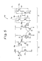
- Figure 5 shows a semiconductor integrated circuit according to another embodiment of the present invention.
- Input means 17 and 18 of this embodiment are more powerful in amplifying input signals IN1 and IN2 than those of the previous embodiment.
- a level changing semiconductor integrated circuit 40 of Fig. 5 has the differential amplifying function explained with reference to Fig. 2, and involves the first and second input means 17 and 18 that are identically formed.
- the input means 17 (18) comprises a first circuit T1 and a second circuit T2 that are connected in parallel with each other.
- the first circuit T1 involves a fifth MOSFET 21 of first conduction type and a seventh MOSFET 23 of second conduction type that are connected in series.
- One end of the fifth MOSFET 21 is connected to a high-potential power source Vcc
- one end of the seventh MOSFET 23 is connected to a low-potential power source Vss.
- the second circuit T2 involves a sixth MOSFET 20 of the first conduction type and an eighth MOSFET 22 of the second conduction type that are connected in series.
- One end of the sixth MOSFET 20 is connected to the high-potential power source Vcc
- one end of the eighth MOSFET 22 is connected to the low-potential power source Vss.
- the gates of the seventh and eighth MOSFETs 23 and 22 are connected to each other.
- the gate of the seventh MOSFET 23 is connected to a node between the fifth and seventh MOSFETs 21 and 23.
- a node between the sixth and eighth MOSFETs 20 and 22 forms an output portion N52 (N52′) of the input means 17 (18).
- the gates of the fifth and sixth MOSFETs 21 and 20 are input terminals B and A to which two kinds of input signals having different signal levels are applied.
- the output portion N52 of the first input means 17 is connected to the base of a first bipolar transistor 13, and the output portion N52′ of the second input means 18 is connected to the base of a second bipolar transistor 14.
- the gate (the input terminal A) of the sixth MOSFET 20 receives a first input signal IN1
- the gate (the input terminal B) of the fifth MOSFET 21 receives a second input signal IN2.
- the gate (the input terminal A) of the sixth MOSFET 20 receives the second input signal IN2
- the gate (the input terminal B) of the fifth MOSFET 21 receives the first input signal IN1.
- the input means 17 (18) of this embodiment will be explained next.
- the MOSFET of the first conduction type is a P-channel MOSFET
- the MOSFET of the second conduction type is an N-channel MOSFET. It is naturally possible that the MOSFET of the first conduction type can be an N-channel MOSFET, and the MOSFET of the second conduction type can be a P-channel MOSFET.
- the input signals IN1 and IN2 supplied to the input terminals A and B of the input means 17 (18) have two kinds of signal levels as in the previous embodiment.
- the drains of the PMOS transistors 20 and 21 are connected to the high-potential power source Vcc.
- the sources of the NMOS transistors 22 and 23 are grounded, i.e., connected to the low-potential power source Vss.
- the input signal IN1 is 4 V
- the input signal IN2 is 3.1 V. These input signals alternately take these two levels.
- the input terminal A receives the input signal IN1
- the input terminal B receives the input signal IN2.
- the input terminal A receives the input signal IN2
- the input terminal B receives the input signal IN1.
- the PMOS transistor 21 When the input signal IN2 becomes L and the input signal IN1 H, the PMOS transistor 21 is turned ON, thereby turning ON the NMOS transistors 23 and 22, and the PMOS transistor 20 is turned OFF to set the node N52 to L (for example, 0 V).
- the levels of the input signals IN1 and IN2 are amplified between 0 V an Vcc, and are output from the node N52.
- the digital input signals IN1 and IN2 are oppositely provided to the input means 17 and 18 to produce the above-mentioned operations.
- the node N52 provides, in response to the level of the signal IN1, a signal of the same logic to the differential amplifier circuit 40.
- the node N52′ provides a logic opposite to the level of the input signal IN1.
- the node N52 When the input signal IN2 changes from L to H, the node N52 provides a signal that changes to H, to the base of the first bipolar transistor 13 of the differential amplifier circuit 40. As a result, the first bipolar transistor 13 is turned ON at once to set the node N31 to H. The level H of the node N31 is applied to the gate of a second NMOS transistor 16 to turn ON the same. This puts the other node N32 at L.
- the input signal IN2 changes from L to H
- the input signal IN1 becomes L and is applied to the gate of the PMOS transistor 20.
- the PMOS transistor 20 is turned ON to increase the potential of the node N52.
- the bipolar transistor 13 is turned ON to increase the potential of the node N31 to H. Namely, the bipolar transistor 13 can pull up the node N31 faster than the PMOS transistor 20 increases the potential of the node N52.
- a bipolar transistor has a collector current that changes exponentially in response to changes in Vbe, and presents a high mutual conductance gm.
- a MOS transistor has a channel current that changes as a square of a gate voltage, and presents a low mutual conductance gm. In this way, the bipolar transistor has excellent charging and discharging characteristics of a load capacity, compared with the MOS transistor.
- the node N52′ provides a signal that changes to H, to the base of the second bipolar transistor 14 of the differential amplifier circuit 40.
- the node N32 is pulled up faster than in the conventional circuit.
- the node N52 When the input signal IN1 changes from H to L, the node N52 provides a signal that changes to L, to the base of the first bipolar transistor 13 of the differential amplifier circuit 40. Due to this, the first bipolar transistor 13 turns OFF at once.
- a signal that changes to H is applied to the node N52′, so that the second bipolar transistor 14 turns ON at once.
- the potential of the gate of the first NMOS transistor 15 increases to turn ON the same.
- the node N31 therefore, drops to L at once.
- the second bipolar transistor 14 immediately turns ON when the node N52′ changes to H, to turn ON the first NMOS transistor 15, thereby immediately dropping the level of the node N31 for the same reasons mentioned above. Namely, to drop the levels of the nodes N31 and N32, the cross-coupled first and second NMOS transistors 15 and 16 are turned ON to realize a high-speed operation.
- each of the input means 17 and 18 of this embodiment includes the MOS transistors 20, 21, 22, and 23, a power source and a temperature margin may be of large sizes.
- the differential amplifier circuit 40 includes the bipolar transistors 13 and 14 to properly use the high-speed characteristics of the bipolar transistors, thereby realizing a very high-speed operation.
- the present invention has been applied to a semiconductor memory.
- the present invention is also applicable, as a differential amplifier circuit, to other semiconductor integrated circuit devices.
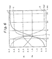
- Figure 6 is a graph showing the effect of the present invention in improving the switching speed of a semiconductor integrated circuit, compared with that of the conventional circuit.
- an input signal IN1 a high level signal
- an input signal IN2 a low level signal
- the conventional circuit provides outputs Vout and inverted Vout indicated by curves C and D, respectively.
- the curves C and D are obtuse.
- the amount of time necessary for increasing or decreasing an output voltage from 1.0 V to 3.0 V is 4.5 nsec on the curves C and D of the conventional circuit.
- the circuit device of the present invention indicated with curves E and F shows a switching speed of 2.5 nsec for the same interval from 1.0 V to 3.0 V, although it shows some decrease in output voltage difference. In this way, the present invention can improve operational speed.
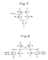
- a circuit as shown in Figure 7 can be used as both the first and second input means.
- P channel type MOSFET 71 and N channel type MOSFET 72 are connected in series to form a first current path and one terminal of the P channel type MOSFET 71 is connected to a high-potential power source while P channel type MOSFET 73 and N channel type MOSFET 74 are connected in series to form a first current path and one terminal of the P channel type MOSFET 71 is connected to a high-potential power source.
- Another MOSFET 75 is provided, one terminal of the MOSFET 75 being connected to a low-potential power source and other terminal thereof is connected to both other terminals of the MOSFETs 72 and 74 while both gates of the MOSFETs 71 and 73 are connected to the gate of the MOSFET 75.
- the construction of the circuit is such that connecting portions of the bipolar transistor and the MOSFET to the high-potential power source and the low-potential power source respectively are reversed to that of the circuit as shown in Figure 2.
- the level changing semiconductor integrated circuit 40 comprises a first current path 11 involving a first bipolar transistor 13 and a first MOSFET 15 that are connected in series, the collector of said first bipolar transistor 13 being connected to one terminal of said first MOSFET 15, the other terminal of said first MOSFET 15 being connected to the high-potential power source, the emitter of said bipolar transistor 13 being connected to the low-potential power source and a second current path I2 involving a first bipolar transistor 14 and a first MOSFET 16 that are connected in series, the collector of said first bipolar transistor 14 being connected to one terminal of said first MOSFET 16, the other terminal of said first MOSFET 16 being connected to the high-potential power source, the emitter of said bipolar transistor 14 being connected to the low-potential power source and further the gates of both MOSFETs 15 and 16 are cross-connected to the corrector of the bipolar transistor 14 and 13 arranged in the opposite current path, respectively.
- P channel type MOSFETs are used but opposite type of MOSFETs may be used if a case requires.
- an emitter length of a bi-polar transistor was solidly fixed at 20 ⁇ m and a gate width W of the N channel MOSFET was fixed at 0.8 ⁇ m while a gate width of the P channel MOSFET was fixed at 1.1 ⁇ m.
- a gate length L of both N channel and P channel MOSFETs were varied from 10 to 50 ⁇ m.
- loads connected to both outputs of the level changing semiconductor integrated circuit 40 were changed from 0.5 pf to 20 pf, respectively.
- the switching speed in this test was determined by measuring a time when an output signal level thereof is changed from lower-most level, for example, 0 V up to 3 V or from higher-most level, for example, 4.2 V down to 1 V.
- the semiconductor integrated circuit device of the present invention can be used in a wide range of applications in which a change in a voltage level of an output signal output from a certain circuit should be transmitted to a successive circuit located down stream of the circuit as quick as possible.
- Figures 10 and 11 show one example of the applications of the present invention in which the semiconductor integrated circuit device of the present invention is used as a level change circuit amplifying outputs output from a sense amplifier with high speed.
- FIG. 10 shows a block diagram of a part of a conventional memory circuit and only two memory cells 104 of the memory circuit are indicated.
- a pair of output signals A and A both of which being complementary signal each other and output from one of the memory circuits are controlled, for example, by address signals A0, A1, ----A19 through a controlling circuit 101, row and column decoders 102 and 103 and a write amplifier 105.
- Fig. 11 shows one example of a circuit diagram illustrating how the inputs of the semiconductor integrated circuit device of the present invention are connected to the outputs of the memory circuit and how the outputs of the integrated circuit device of the present invention are connected to a successive circuit.
- the output signals A and A of the memory circuit are first input to a local sense amplifier 106 simultaneously and successively the outputs thereof are input to a main sense amplifier 107.
- the output signals output from the main sense amplifier 107 are input to input terminals IN1 and IN2 of the integrated circuit device 110 of the present invention, respectively, through a level shifting circuit 108 comprising a bipolar transistor TR1, two diodes D1 and D2 which are connected in series with each other.
- this level shifting circuit 108 another MOSFET transistor TR2 is provided serving as a constant current source.
- one of the output signals A output from the main sense amplifier is input to both an input terminal IN1 of a first input means 17 and an input terminal IN1 of a second input means 18 respectively.
- Another output signals A output from the main sense amplifier is input to both an input terminal IN2 of a first input means 17 and an input terminal IN2 of a second input means 18, respectively.
- outputs of the integrated circuit device 110 of the present invention are output from an output terminal OUT through an output buffer 111 comprising a flip-flop circuit.
- the present invention can have a large power source and a large temperature margin.
- the present invention properly uses bipolar transistors and their high-speed operation characteristics, thereby realizing a high-speed differential amplifier circuit.
Landscapes
- Engineering & Computer Science (AREA)
- Microelectronics & Electronic Packaging (AREA)
- Computer Hardware Design (AREA)
- Logic Circuits (AREA)
- Amplifiers (AREA)
Applications Claiming Priority (4)
| Application Number | Priority Date | Filing Date | Title |
|---|---|---|---|
| JP2002729A JPH03207112A (ja) | 1990-01-10 | 1990-01-10 | 半導体集積回路装置 |
| JP2728/90 | 1990-01-10 | ||
| JP2002728A JPH03207093A (ja) | 1990-01-10 | 1990-01-10 | 半導体集積回路装置 |
| JP2729/90 | 1990-01-10 |
Publications (2)
| Publication Number | Publication Date |
|---|---|
| EP0437402A2 true EP0437402A2 (fr) | 1991-07-17 |
| EP0437402A3 EP0437402A3 (en) | 1992-10-21 |
Family
ID=26336189
Family Applications (1)
| Application Number | Title | Priority Date | Filing Date |
|---|---|---|---|
| EP19910400043 Withdrawn EP0437402A3 (en) | 1990-01-10 | 1991-01-10 | Semiconductor integrated circuit device |
Country Status (3)
| Country | Link |
|---|---|
| US (1) | US5134319A (fr) |
| EP (1) | EP0437402A3 (fr) |
| KR (1) | KR940010834B1 (fr) |
Families Citing this family (7)
| Publication number | Priority date | Publication date | Assignee | Title |
|---|---|---|---|---|
| US5289414A (en) * | 1991-09-27 | 1994-02-22 | Matsushita Electric Industrial Co., Ltd. | Comparator |
| JPH05218872A (ja) * | 1992-01-20 | 1993-08-27 | Nec Corp | コンパレータ回路とその駆動方法 |
| JP2765346B2 (ja) * | 1992-03-18 | 1998-06-11 | 三菱電機株式会社 | バイモス増幅装置 |
| GB9320246D0 (en) * | 1993-10-01 | 1993-11-17 | Sgs Thomson Microelectronics | A driver circuit |
| KR0145855B1 (ko) * | 1995-04-28 | 1998-11-02 | 김광호 | 반도체 메모리장치의 전류센스앰프회로 |
| US6781445B2 (en) * | 2001-04-13 | 2004-08-24 | Zeevo, Inc. | Low power large signal RF tuned buffer amplifier |
| US8477833B2 (en) * | 2009-02-06 | 2013-07-02 | International Business Machines Corporation | Circuits and methods for DFE with reduced area and power consumption |
Family Cites Families (5)
| Publication number | Priority date | Publication date | Assignee | Title |
|---|---|---|---|---|
| US4334293A (en) * | 1978-07-19 | 1982-06-08 | Texas Instruments Incorporated | Semiconductor memory cell with clocked voltage supply from data lines |
| US4349894A (en) * | 1978-07-19 | 1982-09-14 | Texas Instruments Incorporated | Semiconductor memory cell with synthesized load resistors |
| JPH061901B2 (ja) * | 1982-08-16 | 1994-01-05 | 株式会社日立製作所 | Mosトランジスタを用いたバツフア回路 |
| KR910002967B1 (ko) * | 1986-12-12 | 1991-05-11 | 가부시끼가이샤 히다찌세이사꾸쇼 | 바이폴라 트랜지스터와 mos 트랜지스터를 조합한 반도체 집적회로 |
| JPH01184694A (ja) * | 1988-01-11 | 1989-07-24 | Fujitsu Ltd | 信号線切り替え回路 |
-
1991
- 1991-01-09 US US07/638,917 patent/US5134319A/en not_active Expired - Fee Related
- 1991-01-10 EP EP19910400043 patent/EP0437402A3/en not_active Withdrawn
- 1991-01-10 KR KR1019910000268A patent/KR940010834B1/ko not_active Expired - Fee Related
Also Published As
| Publication number | Publication date |
|---|---|
| US5134319A (en) | 1992-07-28 |
| KR910014944A (ko) | 1991-08-31 |
| KR940010834B1 (ko) | 1994-11-17 |
| EP0437402A3 (en) | 1992-10-21 |
Similar Documents
| Publication | Publication Date | Title |
|---|---|---|
| EP0102643B1 (fr) | Circuit de conversion de niveau | |
| US4584492A (en) | Temperature and process stable MOS input buffer | |
| US5270581A (en) | Semiconductor integrated circuit device having step-down circuit associated with component circuits arranged in low-power consumption manner | |
| JPH08195631A (ja) | センス増幅器 | |
| US5173624A (en) | Level-shifter circuit for high-speed low-power bicmos ecl to cmos input buffers | |
| JP3779341B2 (ja) | 半導体メモリ装置 | |
| US5469097A (en) | Translator circuit with symmetrical switching delays | |
| JP3003625B2 (ja) | Cmlcmos変換回路 | |
| US5134319A (en) | Bicmos differential amplifier having improved switching speed | |
| US7236011B2 (en) | High-speed differential logic buffer | |
| JP3800520B2 (ja) | 半導体集積回路装置と半導体装置 | |
| EP0529545B1 (fr) | Circuits intégrés CMOS pour décalage de niveau | |
| US5225717A (en) | BiCMOS input buffer circuit operable at high speed under less power consumption | |
| EP0403174B1 (fr) | Circuit amplificateur différentiel à grande vitesse de fonctionnement | |
| US5532628A (en) | Fast comparator circuit | |
| KR0178276B1 (ko) | 차동증폭회로 | |
| US5412607A (en) | Semiconductor memory device | |
| US5384503A (en) | SRAM with current-mode read data path | |
| JPH08251007A (ja) | BiCMOS論理ゲート回路 | |
| US6064613A (en) | Pre-sense amplifier with reduced output swing | |
| US5077492A (en) | Bicmos circuitry having a combination cmos gate and a bipolar transistor | |
| JP3037177B2 (ja) | 遅延回路 | |
| US6424183B1 (en) | Current comparator | |
| JPS63263824A (ja) | 振幅変換回路 | |
| JPH01164119A (ja) | レベル変換入力回路 |
Legal Events
| Date | Code | Title | Description |
|---|---|---|---|
| PUAI | Public reference made under article 153(3) epc to a published international application that has entered the european phase |
Free format text: ORIGINAL CODE: 0009012 |
|
| AK | Designated contracting states |
Kind code of ref document: A2 Designated state(s): DE FR GB |
|
| RAP1 | Party data changed (applicant data changed or rights of an application transferred) |
Owner name: FUJITSU VLSI LIMITED Owner name: FUJITSU LIMITED |
|
| PUAL | Search report despatched |
Free format text: ORIGINAL CODE: 0009013 |
|
| AK | Designated contracting states |
Kind code of ref document: A3 Designated state(s): DE FR GB |
|
| 17P | Request for examination filed |
Effective date: 19930406 |
|
| 17Q | First examination report despatched |
Effective date: 19950201 |
|
| STAA | Information on the status of an ep patent application or granted ep patent |
Free format text: STATUS: THE APPLICATION IS DEEMED TO BE WITHDRAWN |
|
| 18D | Application deemed to be withdrawn |
Effective date: 19960905 |