EP0438706A2 - Circuit d'attaque CMOS à haute vitesse de commutation - Google Patents
Circuit d'attaque CMOS à haute vitesse de commutation Download PDFInfo
- Publication number
- EP0438706A2 EP0438706A2 EP90124056A EP90124056A EP0438706A2 EP 0438706 A2 EP0438706 A2 EP 0438706A2 EP 90124056 A EP90124056 A EP 90124056A EP 90124056 A EP90124056 A EP 90124056A EP 0438706 A2 EP0438706 A2 EP 0438706A2
- Authority
- EP
- European Patent Office
- Prior art keywords
- cmos
- channel
- devices
- circuit
- logic
- Prior art date
- Legal status (The legal status is an assumption and is not a legal conclusion. Google has not performed a legal analysis and makes no representation as to the accuracy of the status listed.)
- Granted
Links
Images





Classifications
-
- H—ELECTRICITY
- H03—ELECTRONIC CIRCUITRY
- H03K—PULSE TECHNIQUE
- H03K3/00—Circuits for generating electric pulses; Monostable, bistable or multistable circuits
- H03K3/01—Details
- H03K3/011—Modifications of generator to compensate for variations in physical values, e.g. voltage, temperature
-
- H—ELECTRICITY
- H03—ELECTRONIC CIRCUITRY
- H03K—PULSE TECHNIQUE
- H03K17/00—Electronic switching or gating, i.e. not by contact-making and –breaking
- H03K17/14—Modifications for compensating variations of physical values, e.g. of temperature
- H03K17/145—Modifications for compensating variations of physical values, e.g. of temperature in field-effect transistor switches
-
- H—ELECTRICITY
- H03—ELECTRONIC CIRCUITRY
- H03K—PULSE TECHNIQUE
- H03K19/00—Logic circuits, i.e. having at least two inputs acting on one output; Inverting circuits
- H03K19/0175—Coupling arrangements; Interface arrangements
- H03K19/0185—Coupling arrangements; Interface arrangements using field effect transistors only
- H03K19/018507—Interface arrangements
- H03K19/018521—Interface arrangements of complementary type, e.g. CMOS
-
- H—ELECTRICITY
- H03—ELECTRONIC CIRCUITRY
- H03K—PULSE TECHNIQUE
- H03K3/00—Circuits for generating electric pulses; Monostable, bistable or multistable circuits
- H03K3/02—Generators characterised by the type of circuit or by the means used for producing pulses
- H03K3/353—Generators characterised by the type of circuit or by the means used for producing pulses by the use, as active elements, of field-effect transistors with internal or external positive feedback
- H03K3/356—Bistable circuits
- H03K3/356104—Bistable circuits using complementary field-effect transistors
- H03K3/356113—Bistable circuits using complementary field-effect transistors using additional transistors in the input circuit
Definitions
- the present invention relates to high speed CMOS logic circuits. Specifically, a CMOS logic circuit is described for converting CMOS signal levels to small signal levels such as ECL logic signal levels.
- ECL emitter coupled logic circuits
- CMOS technology is progressing to the point where unloaded circuits switch at speeds in the region of .10 nanoseconds.
- CMOS SRAM memory access times of under 10 nanoseconds are achievable.
- the improvement in CMOS devices has made these higher speed circuits and memories possible. With the CMOS device speed approaching that of ECL logic, it would therefore be advantageous to operate the CMOS circuits at ECL signal levels.
- ECL signal levels are much lower than typical CMOS circuit signal levels.
- ECL logic can switch at much higher speeds than CMOS logic elements.
- CMOS circuits, operating at their conventional CMOS power supply voltage levels, while at the same time producing ECL-compatible signal levels would obtain the benefits of the traditionally faster switching ECL circuits while retaining the cost advantages of CMOS-implemented circuit devices.
- CMOS circuits which must be controlled include device delay, as well as slew rate. Circuit delay should be limited in order to preserve the desirable high switching speeds. However, this goal may be adverse to maintaining slew rates at a level which would not exceed 1 volt per nanosecond, for example. As is known to skilled circuit designers, excessive slew rates will generate excessive noise which may interfere with circuit operation.
- CMOS ECL off-chip driver circuit The device is completely fabricated in CMOS technology, using standard CMOS operating potentials Vdd - Vss.
- the circuit is capable of providing smaller ECL-compatible signal levels from CMOS logic signals, having a voltage swing much less than conventional CMOS logic levels.
- the circuit is capable of driving normally encountered transmission line structures interconnecting ECL circuits, and still maintain signal voltage level stability.
- the reduced ECL-compatible signal levels are maintained stable through the use of a feedback path connected between the gates of a P channel and N channel device, serially connected between the CMOS power supply terminals, and an output signal function formed at the series connection of the N channel and P channel devices.
- the feedback devices will permit the output signal junction node to be switched between first and second ECL compatible voltage levels, holding the output junction node at the required ECL signal level.
- an output load element is included at the output junction to provide a substantially constant impedance to the device, further insuring level control of the output signal level in the face of different terminating characteristics for the device.
- a P channel device and an N channel CMOS device are connected in parallel between the output junction and the gate connections of the two serially-connected P channel and N channel output devices.
- One or the other of such feedback devices will be conducting so as to control the voltage level applied to the gates in a direction to maintain small signal levels at the output junction.
- Ample current is supplied by the two P and N channel devices to any expected load, which may be connected to the output junction.
- a slew rate, output level control and circuit delay may all be optimized depending on a particular application.
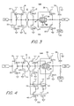
- CMOS off-chip driver (OCD) circuit in accordance with the present invention, which will provide for ECL-compatible small signal levels.
- the circuits shown are designed for implementation in .5 micrometer channel length, 3.6 volt CMOS technology. The invention is not limited to this particular selection of power supply voltage.
- the circuits shown operate from conventional CMOS power supplies represented by terminals Vdd and Vss.
- the input signals to the circuits are CMOS logic levels connected through a circuit pad 24.
- the CMOS portion shown is itself exemplary, and not indicative of any limitation as to CMOS circuitry which might be used to develop the compatible ECL signal levels.
- Each of the devices shown includes a CMOS portion having an output node A.
- the particular implementation shown in the Figs. includes a latch 11 having a pair of P channel, field effect transistors 12 and 16, serially connected with N channel, field effect transistors 13 and 15. These field effect transistors which are used in implementing the invention are hereinafter referred to as a P channel device or an N channel device, as is conventional with CMOS circuit design literature.
- Also shown in the Figs. is the channel length to width dimensions for each of the selected devices which are exemplary only for implementing the present invention for the 3.6 volt power supply, Vdd, Vss.
- the latch 11 is driven by a series combination of P channel device 19 and N channel device 20. These devices have common gate connections which are connected to a circuit pad 24 connected to a source of logic signals operating at the CMOS signal levels. CMOS logic levels are produced on node 1, the junction of devices 19 and 20.
- the signal level established on node A is connected by the output devices comprising a P channel device 26 and N channel device 27 having the shown dimensions to the output node 34.
- a load is illustrated as comprising a linear resistance 37 connected between a source of reference potential pad 35 and the output node 34. As is known in conventional bipolar technology, such a voltage reference would normally be available which establishes a reference voltage roughly midway between the power supply and ground levels in IBM systems.
- a capacitance 36 is shown representing the package and transmission line capacitance terminating the device output pad 34.
- the ECL-compatible output voltage for the device appears at the junction of each of the P channel and N channel devices 26 and 27.
- CMOS logic circuit 11 has output devices 12 and 13 dimensioned to provide nominal output signal levels which are approximately 1.0 and -1.5 volts. Nominal CMOS levels in this configuration would be 1.4 volts and -2.2 volts. Thus, CMOS logic circuit 11 produces signal levels intermediate to CMOS logic levels and ECL logic levels.
- the compatible ECL logic voltage levels are selected to be +.5 and -.5 volts.
- the aforesaid reference potential is 0 volts which is used in IBM implemented bipolar technology to distinguish between a logic 1 and logic 0 condition for the ECL logic states.
- the feedback transistors 29 and 30 are employed. Each of the feedback transistors 29 and 30 participate in various degrees in the different embodiments in forming a voltage divider with P channel devices 12, 26 and N channel devices 13, 27, depending on the logic state at node A.
- the voltage at node A will force one of the p channel and N channel devices 29 and 30 to conduct substantially more current than the remaining device.
- Node A will have a nominal voltage level about .5 volts less than the standard CMOS logic up level and about .5 V greater than the standard CMOS logic down level.
- the P channel device 26 or N channel device 27 will conduct current.
- the voltage which is developed at the junction of these two P channel and N channel devices 26 and 27 is in part determined by the feedback device 29 or 30.
- the feedback devices 29 and 30 will cause the voltage at the gate connections to P channel device 26 and N channel device 27 to change in a direction to compensate for any changes in output signal level.
- a logic 1 ECL level in the example of Fig. 1 a lowering of the potential at output pad 34 will tend to lower the voltage at node A which will turn device 26 on more, increasing the output voltage level on output pad 34 to an ECL-compatible voltage.
- negative feedback through the P channel device 30 will adjust the voltage at node A and the gate of N channel device 27 so as to maintain the desired ECL voltage level on output pad 34.
- circuits of Figs. 1 and 2 illustrate implementations where the gates of the feedback devices 29 and 30 are connected together to either the output pad 34 or the input node A. In the circuits of Figs. 3 and 4, these gates are returned to a higher potential, corresponding to Vdd and Vss, which provide certain advantages and disadvantages with respect to the implementations of Figs. 1 and 2.
- devices 29 and 30 are fully turned on, which assist in making each of the transistors smaller, providing an overall improvement in the transient response for the device.
- the feedback devices 29 and 30 are shown connected to pairs of serially connected P channel and N channel devices 40, 41 and 42, 43.
- All the circuits shown in Figs. 1-4 have a regulated ECL-compatible logic level output.
- the +.5 and -.5 voltage potentials are regulated against process variations which occur in the manufacture of CMOS devices.
- variations in the channel length, width and device thresholds may occur varying the circuit performance.
- changes in the CMOS power supply levels Vdd and Vss will adversely effect the logic levels.
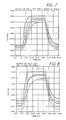
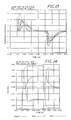
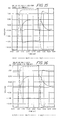
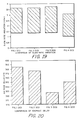
- Performance of the circuits in Figs. 1-4 was evaluated with respect to the ability of the circuit to maintain the ECL-compatible logic level voltages at their nominal values of +.5 and -.5 volts, the respective slew rates for the circuits, and the respective propagation delays for switching each of the circuits.
- the circuit performance was evaluated under the conditions of process variations and power supply variations shown in Table 1 below. The circuit performance for these conditions is depicted in the graphs of Figs. 6-17.
- the feedback path for a "1" ECL output level will be through P channel device 26 and N channel device 29 and N channel device 13.
- Node A will maintain the ECL-compatible logic voltage appearing at the junction of devices 26 and 27 with the above variations.
- the feedback path is through device 27, device 30 and device 12.
- the potential on node A will maintain the ECL logic state "0" voltage level at its nominal value. In this condition, any potential change at the junction of P channel devices 26 and 27 is compensated for by more or less voltage being applied to the gate of device 27.
- Fig. 4 provides voltage stability for the generated ECL-compatible output levels which is superior to the embodiments of Figs. 1, 2 and 3. It can be seen from Fig. 9 that the variations in output logic levels are much smaller for this embodiment.
- FIG. 10-13 Slew rate performance can be illustrated for each of the embodiments of Figs. 1-4 by referring to Figs. 10-13. These Figs. illustrate how the slew rate for all the process and power supply variations represented in Table 1 are effected. As can be seen from Fig. 13, the magnitude of the slew rate change for the circuit of Fig. 4 is superior for the various process and power supply variations represented by Table 1.
- Fig. 4 represents the best overall solution to balancing the requirements for slew rate, delay and output level control in the various embodiments.
- FIG. 5 illustrates how an 80 Ohm impedance may be constructed, which is substantially resistive using two additional devices, P channel device 45 and N channel device 46. These devices will track the electrical performance of the remaining devices of the circuit and help to compensate for device variation.
- devices 45 and 46 provide an almost linear resistance over the range of voltage that occurs.
- CMOS logic circuits of Figs. 1-4 may be implemented in place of conventional ECL drive circuits, operating from standard CMOS logic power supply levels.
- the resulting compatible bipolar logic levels have a controlled output level, as well as slew rate and delay parameters compatible with ECL technology.
Landscapes
- Engineering & Computer Science (AREA)
- Computer Hardware Design (AREA)
- Physics & Mathematics (AREA)
- Computing Systems (AREA)
- General Engineering & Computer Science (AREA)
- Mathematical Physics (AREA)
- Logic Circuits (AREA)
Applications Claiming Priority (2)
| Application Number | Priority Date | Filing Date | Title |
|---|---|---|---|
| US07/471,155 US4998028A (en) | 1990-01-26 | 1990-01-26 | High speed CMOS logic device for providing ECL compatible logic levels |
| US471155 | 1990-01-26 |
Publications (3)
| Publication Number | Publication Date |
|---|---|
| EP0438706A2 true EP0438706A2 (fr) | 1991-07-31 |
| EP0438706A3 EP0438706A3 (en) | 1992-01-29 |
| EP0438706B1 EP0438706B1 (fr) | 1995-03-22 |
Family
ID=23870466
Family Applications (1)
| Application Number | Title | Priority Date | Filing Date |
|---|---|---|---|
| EP90124056A Expired - Lifetime EP0438706B1 (fr) | 1990-01-26 | 1990-12-13 | Circuit d'attaque CMOS à haute vitesse de commutation |
Country Status (4)
| Country | Link |
|---|---|
| US (1) | US4998028A (fr) |
| EP (1) | EP0438706B1 (fr) |
| JP (1) | JP2536965B2 (fr) |
| DE (1) | DE69018053T2 (fr) |
Cited By (4)
| Publication number | Priority date | Publication date | Assignee | Title |
|---|---|---|---|---|
| US6054874A (en) * | 1997-07-02 | 2000-04-25 | Cypress Semiconductor Corp. | Output driver circuit with switched current source |
| US6084439A (en) * | 1997-07-02 | 2000-07-04 | Cypress Semiconductor Corp. | Peak detector circuit with extended input voltage range |
| WO2000077931A1 (fr) * | 1999-06-10 | 2000-12-21 | Telefonaktiebolaget Lm Ericsson | Amplificateur |
| EP0936526A3 (fr) * | 1998-01-20 | 2001-10-17 | Siemens Aktiengesellschaft | Générateur de tension de référence |
Families Citing this family (7)
| Publication number | Priority date | Publication date | Assignee | Title |
|---|---|---|---|---|
| US5247212A (en) * | 1991-01-31 | 1993-09-21 | Thunderbird Technologies, Inc. | Complementary logic input parallel (clip) logic circuit family |
| JP2824706B2 (ja) * | 1991-09-27 | 1998-11-18 | 三菱電機株式会社 | 電流源回路およびその動作方法 |
| US5280204A (en) * | 1992-07-02 | 1994-01-18 | International Business Machines Corporation | ECI compatible CMOS off-chip driver using feedback to set output levels |
| TW247975B (fr) * | 1992-07-14 | 1995-05-21 | Philips Electronics Nv | |
| JP3080793B2 (ja) * | 1992-10-27 | 2000-08-28 | 株式会社東芝 | インターフェース回路 |
| US5343094A (en) * | 1993-01-13 | 1994-08-30 | National Semiconductor Corporation | Low noise logic amplifier with nondifferential to differential conversion |
| US5365127A (en) * | 1993-10-18 | 1994-11-15 | Hewlett-Packard Company | Circuit for conversion from CMOS voltage levels to shifted ECL voltage levels with process compensation |
Family Cites Families (9)
| Publication number | Priority date | Publication date | Assignee | Title |
|---|---|---|---|---|
| US3986043A (en) * | 1974-12-20 | 1976-10-12 | International Business Machines Corporation | CMOS digital circuits with active shunt feedback amplifier |
| JPH0773205B2 (ja) * | 1983-12-20 | 1995-08-02 | 株式会社日立製作所 | レベル変換回路 |
| US4656372A (en) * | 1985-11-25 | 1987-04-07 | Ncr Corporation | CMOS to ECL interface circuit |
| US4656375A (en) * | 1985-12-16 | 1987-04-07 | Ncr Corporation | Temperature compensated CMOS to ECL translator |
| DE3784285T2 (de) * | 1986-08-29 | 1993-07-22 | Mitsubishi Electric Corp | Integrierte komplementaere mos-schaltung. |
| US4845381A (en) * | 1987-10-01 | 1989-07-04 | Vlsi Technology, Inc. | Voltage level shifting circuit |
| US4835419A (en) * | 1987-10-30 | 1989-05-30 | International Business Machines Corporation | Source-follower emitter-coupled-logic receiver circuit |
| JPH01138813A (ja) * | 1987-11-26 | 1989-05-31 | Toshiba Corp | Ecl―cmosレベル変換回路 |
| US4947061A (en) * | 1989-02-13 | 1990-08-07 | At&T Bell Laboratories | CMOS to ECL output buffer circuit |
-
1990
- 1990-01-26 US US07/471,155 patent/US4998028A/en not_active Expired - Fee Related
- 1990-11-30 JP JP2337038A patent/JP2536965B2/ja not_active Expired - Lifetime
- 1990-12-13 EP EP90124056A patent/EP0438706B1/fr not_active Expired - Lifetime
- 1990-12-13 DE DE69018053T patent/DE69018053T2/de not_active Expired - Fee Related
Cited By (5)
| Publication number | Priority date | Publication date | Assignee | Title |
|---|---|---|---|---|
| US6054874A (en) * | 1997-07-02 | 2000-04-25 | Cypress Semiconductor Corp. | Output driver circuit with switched current source |
| US6084439A (en) * | 1997-07-02 | 2000-07-04 | Cypress Semiconductor Corp. | Peak detector circuit with extended input voltage range |
| EP0936526A3 (fr) * | 1998-01-20 | 2001-10-17 | Siemens Aktiengesellschaft | Générateur de tension de référence |
| WO2000077931A1 (fr) * | 1999-06-10 | 2000-12-21 | Telefonaktiebolaget Lm Ericsson | Amplificateur |
| US6603347B2 (en) | 1999-06-10 | 2003-08-05 | Telefonaktiebolaget Lm Ericsson (Publ) | Amplifier having controllable input impedance |
Also Published As
| Publication number | Publication date |
|---|---|
| US4998028A (en) | 1991-03-05 |
| DE69018053D1 (de) | 1995-04-27 |
| JP2536965B2 (ja) | 1996-09-25 |
| DE69018053T2 (de) | 1995-09-28 |
| EP0438706B1 (fr) | 1995-03-22 |
| JPH03240315A (ja) | 1991-10-25 |
| EP0438706A3 (en) | 1992-01-29 |
Similar Documents
| Publication | Publication Date | Title |
|---|---|---|
| US7078943B2 (en) | Series terminated CMOS output driver with impedance calibration | |
| US6225846B1 (en) | Body voltage controlled semiconductor integrated circuit | |
| EP0554121A2 (fr) | Circuit de terminaison de ligne | |
| US6759875B2 (en) | Voltage controlled oscillation circuit | |
| US4954729A (en) | Output buffer circuit used for stable voltage source | |
| EP0368524A1 (fr) | Circuit de tampon de sortie | |
| KR100243850B1 (ko) | 비휘발성 메모리 집적 회로의 고전압 스위칭용고전압 레벨 시프터 | |
| EP0110701B1 (fr) | Circuit tampon d'entrée | |
| EP0438706B1 (fr) | Circuit d'attaque CMOS à haute vitesse de commutation | |
| US4897564A (en) | BICMOS driver circuit for high density CMOS logic circuits | |
| US4845388A (en) | TTL-CMOS input buffer | |
| JPH0752835B2 (ja) | 多重位相分割器ttl出力回路 | |
| US5384498A (en) | DC-coupled active pull-down ECL circuit with self-adjusting drive capability | |
| US7049890B2 (en) | Operational amplifier with self control circuit for realizing high slew rate throughout full operating range | |
| EP0720296B1 (fr) | Circuit tampon et circuit de polarisation | |
| US5847576A (en) | Low power, variable logic threshold voltage, logic gates | |
| JPH06230840A (ja) | バイアス回路 | |
| US4841172A (en) | Bipolar-MOS logic circuit with high speed operation | |
| JP3438779B2 (ja) | 駆動回路および半導体レーザ駆動装置 | |
| US5574391A (en) | ECL integrated circuit allowing fast operation | |
| KR100420689B1 (ko) | 버퍼회로 | |
| US5070261A (en) | Apparatus and method for translating voltages | |
| EP0420183B1 (fr) | Circuit push-pull | |
| KR100239717B1 (ko) | 데이타 출력버퍼 | |
| JPH01272230A (ja) | 半導体回路装置 |
Legal Events
| Date | Code | Title | Description |
|---|---|---|---|
| PUAI | Public reference made under article 153(3) epc to a published international application that has entered the european phase |
Free format text: ORIGINAL CODE: 0009012 |
|
| AK | Designated contracting states |
Kind code of ref document: A2 Designated state(s): DE FR GB |
|
| PUAL | Search report despatched |
Free format text: ORIGINAL CODE: 0009013 |
|
| 17P | Request for examination filed |
Effective date: 19911112 |
|
| AK | Designated contracting states |
Kind code of ref document: A3 Designated state(s): DE FR GB |
|
| 17Q | First examination report despatched |
Effective date: 19931227 |
|
| GRAA | (expected) grant |
Free format text: ORIGINAL CODE: 0009210 |
|
| AK | Designated contracting states |
Kind code of ref document: B1 Designated state(s): DE FR GB |
|
| REF | Corresponds to: |
Ref document number: 69018053 Country of ref document: DE Date of ref document: 19950427 |
|
| ET | Fr: translation filed | ||
| PGFP | Annual fee paid to national office [announced via postgrant information from national office to epo] |
Ref country code: FR Payment date: 19951128 Year of fee payment: 6 |
|
| PLBE | No opposition filed within time limit |
Free format text: ORIGINAL CODE: 0009261 |
|
| STAA | Information on the status of an ep patent application or granted ep patent |
Free format text: STATUS: NO OPPOSITION FILED WITHIN TIME LIMIT |
|
| 26N | No opposition filed | ||
| PGFP | Annual fee paid to national office [announced via postgrant information from national office to epo] |
Ref country code: GB Payment date: 19961126 Year of fee payment: 7 |
|
| PGFP | Annual fee paid to national office [announced via postgrant information from national office to epo] |
Ref country code: DE Payment date: 19970116 Year of fee payment: 7 |
|
| PG25 | Lapsed in a contracting state [announced via postgrant information from national office to epo] |
Ref country code: FR Effective date: 19970829 |
|
| REG | Reference to a national code |
Ref country code: FR Ref legal event code: ST |
|
| PG25 | Lapsed in a contracting state [announced via postgrant information from national office to epo] |
Ref country code: GB Free format text: LAPSE BECAUSE OF NON-PAYMENT OF DUE FEES Effective date: 19971213 |
|
| GBPC | Gb: european patent ceased through non-payment of renewal fee |
Effective date: 19971213 |
|
| PG25 | Lapsed in a contracting state [announced via postgrant information from national office to epo] |
Ref country code: DE Free format text: LAPSE BECAUSE OF NON-PAYMENT OF DUE FEES Effective date: 19980901 |