EP0439165A2 - Feldeffekttransistor mit vertikaler Struktur und Verfahren zur Herstellung - Google Patents
Feldeffekttransistor mit vertikaler Struktur und Verfahren zur Herstellung Download PDFInfo
- Publication number
- EP0439165A2 EP0439165A2 EP91100893A EP91100893A EP0439165A2 EP 0439165 A2 EP0439165 A2 EP 0439165A2 EP 91100893 A EP91100893 A EP 91100893A EP 91100893 A EP91100893 A EP 91100893A EP 0439165 A2 EP0439165 A2 EP 0439165A2
- Authority
- EP
- European Patent Office
- Prior art keywords
- regions
- pedestal
- pedestal regions
- semiconductor substrate
- gate electrode
- Prior art date
- Legal status (The legal status is an assumption and is not a legal conclusion. Google has not performed a legal analysis and makes no representation as to the accuracy of the status listed.)
- Granted
Links
- 230000005669 field effect Effects 0.000 title claims description 3
- 238000004519 manufacturing process Methods 0.000 title description 6
- NJPPVKZQTLUDBO-UHFFFAOYSA-N novaluron Chemical group C1=C(Cl)C(OC(F)(F)C(OC(F)(F)F)F)=CC=C1NC(=O)NC(=O)C1=C(F)C=CC=C1F NJPPVKZQTLUDBO-UHFFFAOYSA-N 0.000 claims abstract description 73
- 239000000758 substrate Substances 0.000 claims abstract description 26
- 239000004065 semiconductor Substances 0.000 claims abstract description 20
- 239000010410 layer Substances 0.000 description 49
- 238000009792 diffusion process Methods 0.000 description 10
- 238000000034 method Methods 0.000 description 9
- 238000002955 isolation Methods 0.000 description 8
- 238000005229 chemical vapour deposition Methods 0.000 description 5
- 238000005530 etching Methods 0.000 description 4
- 229920002120 photoresistant polymer Polymers 0.000 description 4
- 229910021420 polycrystalline silicon Inorganic materials 0.000 description 4
- 229920005591 polysilicon Polymers 0.000 description 4
- 229910052782 aluminium Inorganic materials 0.000 description 3
- XAGFODPZIPBFFR-UHFFFAOYSA-N aluminium Chemical compound [Al] XAGFODPZIPBFFR-UHFFFAOYSA-N 0.000 description 3
- 229910052751 metal Inorganic materials 0.000 description 3
- 239000002184 metal Substances 0.000 description 3
- 230000003647 oxidation Effects 0.000 description 3
- 238000007254 oxidation reaction Methods 0.000 description 3
- 238000001259 photo etching Methods 0.000 description 3
- 229910001218 Gallium arsenide Inorganic materials 0.000 description 2
- 239000012535 impurity Substances 0.000 description 2
- 230000010354 integration Effects 0.000 description 2
- 230000000873 masking effect Effects 0.000 description 2
- 230000001681 protective effect Effects 0.000 description 2
- 229910052785 arsenic Inorganic materials 0.000 description 1
- RQNWIZPPADIBDY-UHFFFAOYSA-N arsenic atom Chemical compound [As] RQNWIZPPADIBDY-UHFFFAOYSA-N 0.000 description 1
- 238000007493 shaping process Methods 0.000 description 1
- 229910052710 silicon Inorganic materials 0.000 description 1
- 239000010703 silicon Substances 0.000 description 1
- 239000002356 single layer Substances 0.000 description 1
- 238000004544 sputter deposition Methods 0.000 description 1
Images






Classifications
-
- H—ELECTRICITY
- H10—SEMICONDUCTOR DEVICES; ELECTRIC SOLID-STATE DEVICES NOT OTHERWISE PROVIDED FOR
- H10D—INORGANIC ELECTRIC SEMICONDUCTOR DEVICES
- H10D30/00—Field-effect transistors [FET]
- H10D30/60—Insulated-gate field-effect transistors [IGFET]
- H10D30/63—Vertical IGFETs
-
- H—ELECTRICITY
- H10—SEMICONDUCTOR DEVICES; ELECTRIC SOLID-STATE DEVICES NOT OTHERWISE PROVIDED FOR
- H10D—INORGANIC ELECTRIC SEMICONDUCTOR DEVICES
- H10D64/00—Electrodes of devices having potential barriers
- H10D64/20—Electrodes characterised by their shapes, relative sizes or dispositions
- H10D64/27—Electrodes not carrying the current to be rectified, amplified, oscillated or switched, e.g. gates
- H10D64/311—Gate electrodes for field-effect devices
- H10D64/411—Gate electrodes for field-effect devices for FETs
- H10D64/511—Gate electrodes for field-effect devices for FETs for IGFETs
- H10D64/517—Gate electrodes for field-effect devices for FETs for IGFETs characterised by the conducting layers
- H10D64/518—Gate electrodes for field-effect devices for FETs for IGFETs characterised by the conducting layers characterised by their lengths or sectional shapes
Definitions
- the present invention relates to a semiconductor device having an insulated gate transistor, e.g., a MOS transistor and, more particularly, to a semiconductor device with improved current drivability.
- an insulated gate transistor e.g., a MOS transistor
- Fig. 9 is a plan view of the conventional MOS transistor and Fig. 8 is a cross-sectional view taken along line 8 - 8 of Fig. 8.
- an isolation region 102 is formed on the major surface of a p-type substrate 101. In regions isolated by the isolation region are formed n-type source/drain regions 103i and 103 2 .
- a gate insulating layer 104 is formed on the channel region between the source/drain regions 103, and 103 2 .
- a gate electrode 105 is formed on the gate insulating layer 104.
- the source/drain regions 103 1 and 103 2 are formed on both sides of the gate electrode 105.
- the width L of the gate electrode 105 is called the gate length and the width W of each of the source/ drain regions 103 1 and 103 2 in the direction normal to the direction of the channel is called the channel width.
- the channel width W in expression (1) is currently made large. With such an approach, however, an increase of the channel width W results in an increase of the area of the MOS structure, thus making a fine structure of the device difficult.
- a transistor has been developed in which a pedestal region is provided between source and drain regions to protrude from a semiconductor substrate and a gate electrode is formed on side walls of the pedestal region. This transistor is useful for making the device structure fine, but still it has no sufficient current drivability.
- a semiconductor device with a field effect transistor comprising: a semiconductor substrate having a plurality of pedestal regions each consisting of a first surface, a second surface which differ from said first surface in height and side surfaces connecting said first and second surfaces together; first and second regions formed in said first and second surfaces, respectively, of said semiconductor substrate, said first and second regions serving as source/drain regions and being opposite to said semiconductor substrate in conductivity type; and gate electrodes formed on side surfaces of said pedestal regions and linked together.
- a plurality of pedestal regions are formed in a semiconductor substrate and a plurality of transistors having gate electrodes are formed in side surfaces of the pedestal regions.
- the transistors function as a single transistor because their gate electrodes are connected together. Therefore, the channel width of one transistor can be increased, thereby providing high current drivability.
- the transistor of the invention permits high- density integration and moreover the channel width to be increased with a small device area.
- an isolation region 2 is formed on, for example, a p-type substrate 1 by means of, for example, a technique called LOCOS (localized oxidation of silicon).
- LOCOS localized oxidation of silicon
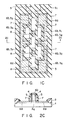
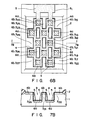
- pedestal regions 3i to 3 7 protruding from the surface of the substrate 1 are formed in rows on a device region 1 by means of, for example, known selective epitaxial growth (SEG). More specifically, the pedestal regions 3 3 to 3 5 are arranged at regularly spaced intervals along the row of the pedestal regions 3 1 and 3 2 which are also arranged at regularly spaced intervals. The pedestal regions 3 6 and 3 7 are also arranged at regularly spaced intervals along the row of the pedestal regions 3i and 3 2 .
- the rows of pedestal regions have an equal space between adjacent pedestal regions.
- the space LD between pedestal regions is shorter than the length LA of each pedestal region.
- the spaced LE between adjacent rows is shorter than the space LD between adjacent pedestal regions.
- an oxide layer serving as a gate insulating layer 4 is formed over the surface of the device region 1 1 including surfaces of the pedestal regions 3 1 to 3 7 by means of, for example, thermal oxidation.
- a polysilicon layer is deposited over the entire surface of the resultant structure by means of, for example, chemical vapor deposition (CVD).
- CVD chemical vapor deposition
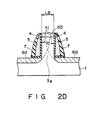
- the polysilicon layer is etched by means of, for example, RIE which is known as an anisotropic etching technique so that it may remain only on side surfaces of the pedestal regions 3i to 3 7 , thereby forming gate electrodes 5.
- the gate electrodes 5 formed on side surfaces of the pedestal regions 3 1 to 3 7 are linked together and serve as a single gate electrode in the device region 1 1 .
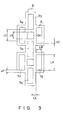
- Fig. 3 is a schematic representation of a plan view of the device in the state of Fig. 1 B.
- the length LA and width LB of the pedestal regions are about 1.4 ⁇ m and 0.5 ⁇ m, respectively.
- the gate insulating layer 4 (not shown in Fig. 3) formed on the surfaces of the pedestal regions has a thickness of about 100 ⁇ m and the gate electrode has a thickness LF of about 0.3 ⁇ m.
- the space LE between the rows of pedestal regions is filled up with the gate electrode 5, it may be set to two or less times the thickness LF of the gate electrode 5. Since the thickness LF of the gate electrode 5 is 0.3 ⁇ m as described above, the space LE may be 0.6 ⁇ m or less. In this embodiment, to ensure a sufficient thickness of the gate electrode 5 on the gate insulating layer 4 between pedestal regions, the space LE is set to be, for example, of the order of 0.5 ⁇ m taking some allowance into account.
- the space LD between the pedestal regions 3 4 and 3 3 arranged in a row be set to at least twice the thickness LF of the gate electrode 5. Since the thickness LF of the gate electrode 5 is 0.3 ⁇ m, if the space LD is 1.0 ⁇ m, then the length LG of each side of the opening CH will be Being very thin, the thickness of the gate insulating layer 4 is neglected here.
- each of the pedestal regions 3 1 , 3 3 and 3 4 is 1.4 ⁇ m, it is required, to secure the spacing LD of 1.0 ⁇ m between the pedestal regions 3 3 and 3 4 , that the length LC of overlap between the pedestal regions 3 1 and 3 3 -(3 4 ) be Since a pedestal region in one row overlaps a pedestal region in another row and the space LE between rows of pedestal regions is set to two or less times that the thickness of the gate electrode 5, the space between each of the pedestal regions and the other can be filled up with the gate electrode 5. Thus, the single gate electrode 5 will suffice for the pedestal regions 3i to 3 7 arranged in rows.
- a mask formed of, for example, a photo resist may be provided on the polysilicon layer 5 formed on the isolation region 2 to thereby form a contact hole 5 1 .
- n-type impurities of, for example, arsenic, which are opposite in conductivity type to the substrate 1 are implanted into the substrate 1 and top portions of the pedestal regions 3i to 3 7 using the gate electrode 5 and the isolation region 2 as a mask, whereby source/drain regions 6a and 6b are formed within the substrate and the top portions of the pedestal regions.
- an oxide layer 7 is formed over the entire surface by means of, for example, CVD. Then, the oxide layer 7 is subjected to anisotropic etching by means of, for example, RIE so that the oxide layer is left on the side walls of the pedestal regions. Thus, the gate electrode 5 is insu-lated from other conductive regions by the oxide layer 7. The removal of the oxide layer 7 to expose the surface of the substrate 1 and the top portions of the pedestal regions 3i to 3 7 permits contact holes 8 to be formed on a self-alignment basis.
- a contact hole (not shown) communicating with the contact area 5i of the gate electrode 5 is formed in the oxide layer 7.
- a conductive layer which is in contact with the source/ drain regions 6a and 6b is formed and then patterned in accordance with a predetermined wiring pattern, and the entire surface of the resultant structure is covered with a surface protective film, whereby a MOS transistor with high current drivability is produced.
- the channel region of the MOS transistor according to the first embodiment is formed of the inside side walls of the pedestal regions 3i to 3 7 .
- the MOS transistor may operate with the diffusion layers 6a within the semiconductor substrate 1 as source/drain and the diffusion layers 6b of the pedestal regions 3i to 3 7 as drain/source or with one of the diffusion layers 6a as source, the other as drain and the diffusion layers 6b of the pedestal regions as a conductive portion for channel-to- channel connection.
- the channel width W of one pedestal region is given by In the present embodiment, there are plural pedestal regions in one device region. Assuming the number of the pedestal regions to be n, then the channel width W per device will be
- the minimum spacing LE between rows of the pedestal regions is selected to be two or less times that the thickness LF of the gate electrode 5 and the pedestal regions in the central row overlap the pedestal regions in other rows, thereby permitting a single gate electrode 5 to connect all of the pedestal regions together.
- a depletion layer is produced within the pedestal region by the gate electrode.
- the gate bias and impurity concentration of the MOS transistor constructed as described above are, for example, 3V, 1 x 10 16 cm- 3 , respectively.
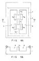
- Figs. 4A, 4B and 4C are plan views, in the order of steps of manufacture, of a semiconductor device according to a second embodiment of the present invention and Figs. 5A, 5B and 5C are cross-sectional views of Figs. 1 A, 1B and 1C.
- Like reference characters are used to designate corresponding parts to those in the first embodiment.
- an isolation region 2 is formed on the major surface of, for example, a p-type substrate 1 by means of, for example, LOCOS.
- a concavity 9 is formed within the substrate 1 by means of a photoetching method using a photo resist.
- the substrate 1 is selectively etched so that pedestal regions 3s to 3 14 protruding from the bottom of the concavity 9 are formed.
- the pedestal regions 3 10 to 3 12 are arranged at regularly spaced intervals along the pedestal regions 3s and 3 9 at regu-larly spaced intervals, and moreover the pedestal regions 3 13 and 3 14 are arranged at regularly spaced intervals along the pedestal regions 3 10 to 3 12 .
- the pedestal regions 3s to 3 14 are arranged in substantially the same relation as in the first embodiment.
- an oxide layer serving as a gate insulating layer is subsequently formed over the surface of the device region including the surfaces of the pedestal regions by means of, for example, thermal oxidation.
- a polysilicon layer which is then subjected to anisotropic etching by means of, for example, RIE to leave it on side walls of the pedestal regions 3 8 to 3 14 and concavity 9, thereby forming gate electrodes 5.
- the area between each of the pedestal regions and another is filled up with the gate electrodes 5 oxide layer is subsequently subjected to anisotropic etching by means of, for example, RIE so that the oxide layer is left on the side walls of the pedestal regions 3 18 to 3 27 as illustrated in Figs. 4C and 5C.
- electrode 5 extending from the substrate 1 to the isolation region 2 is covered with the oxide layer 7 so that it may not exposed.
- the gate electrode 5 is insulated from other conductive regions. If, in this state, the surface of the substrate 1 and the surfaces of the pedestal regions 3i ⁇ to 3 24 are exposed, contact holes 8 can be formed on a self-alignment basis.
- a contact hole (not shown) communicating with the contact area 5 1 of the gate electrode 5 is formed in the oxide layer 7.
- conductive layers which are in contact with the source/drain regions 6a and 6b is formed and then patterned in accordance with a predetermined wiring pattern.
- the entire surface of the resultant structure is covered with a surface protective film, whereby a MOS transistor according to the third embodiment is produced.
- a MOS transistor with higher current drivability and smaller surface area than those of the second and third embodiments can be produced.
- the contact holes for the source/drain diffusion layers 6a and 6b are formed using a self aligned process.
- the contact holes may be formed by a photoetching method using a photo resist, that is, by a masking process.
- an oxide layer 7 is formed over the entire surface of a device which has been produced in accordance with the same steps as those used for producing the structure shown in Figs. 6B and 7B by means of, for example, CVD.
- a contact hole 9 communicating with a source/diffusion layer 6a and a contact hole 10 communicating with a source/drain diffusion layer 6b are formed in the oxide layer 7 by means of a photoetching method using a photo resist.
- the contact holes 9 and 10 are alternately formed in alignment with one another. As can be seen from Fig. 6D, the contact holes 9 are in alignment with one another along a diagonal line and so are the contact holes 10.
- metal lines 11 which contact the source/drain diffusion layers 6a through the contact holes 9 and metal lines 12 which contact the source/drain diffusion layers 6b through the contact holes 10 can be formed.
- the metal lines can be formed by a single layer of aluminum.
- a MOS-FET is produced.
- a MESFET which is formed on a GaAs substrate may be produced.
- a gate insulating layer there is no need for a gate insulating layer.
- GaAs itself is semiinsulating, an isolation region which is represented by a field insulating layer need not necessarily be formed.
Landscapes
- Insulated Gate Type Field-Effect Transistor (AREA)
Applications Claiming Priority (2)
| Application Number | Priority Date | Filing Date | Title |
|---|---|---|---|
| JP2014032A JPH07112067B2 (ja) | 1990-01-24 | 1990-01-24 | 半導体装置 |
| JP14032/90 | 1990-01-24 |
Publications (3)
| Publication Number | Publication Date |
|---|---|
| EP0439165A2 true EP0439165A2 (de) | 1991-07-31 |
| EP0439165A3 EP0439165A3 (en) | 1992-02-05 |
| EP0439165B1 EP0439165B1 (de) | 1996-07-10 |
Family
ID=11849811
Family Applications (1)
| Application Number | Title | Priority Date | Filing Date |
|---|---|---|---|
| EP91100893A Expired - Lifetime EP0439165B1 (de) | 1990-01-24 | 1991-01-24 | Feldeffekttransistor mit vertikaler Struktur und Verfahren zur Herstellung |
Country Status (5)
| Country | Link |
|---|---|
| US (1) | US5185646A (de) |
| EP (1) | EP0439165B1 (de) |
| JP (1) | JPH07112067B2 (de) |
| KR (1) | KR940003604B1 (de) |
| DE (1) | DE69120689T2 (de) |
Cited By (1)
| Publication number | Priority date | Publication date | Assignee | Title |
|---|---|---|---|---|
| US5317184A (en) * | 1992-11-09 | 1994-05-31 | Harris Corporation | Device and method for improving current carrying capability in a semiconductor device |
Families Citing this family (15)
| Publication number | Priority date | Publication date | Assignee | Title |
|---|---|---|---|---|
| JP2748072B2 (ja) * | 1992-07-03 | 1998-05-06 | 三菱電機株式会社 | 半導体装置およびその製造方法 |
| US5453637A (en) * | 1994-05-18 | 1995-09-26 | United Microelectronics Corp. | Read-only memory cell configuration with steep trenches |
| US5936874A (en) | 1997-06-19 | 1999-08-10 | Micron Technology, Inc. | High density semiconductor memory and method of making |
| US5949700A (en) * | 1998-05-26 | 1999-09-07 | International Business Machines Corporation | Five square vertical dynamic random access memory cell |
| US6107133A (en) * | 1998-05-28 | 2000-08-22 | International Business Machines Corporation | Method for making a five square vertical DRAM cell |
| US6225158B1 (en) | 1998-05-28 | 2001-05-01 | International Business Machines Corporation | Trench storage dynamic random access memory cell with vertical transfer device |
| US6538292B2 (en) * | 2001-03-29 | 2003-03-25 | Macronix International Co. Ltd. | Twin bit cell flash memory device |
| KR100753098B1 (ko) * | 2004-12-28 | 2007-08-29 | 주식회사 하이닉스반도체 | 채널길이를 증가시킨 반도체 소자 및 그의 제조 방법 |
| US7491995B2 (en) | 2006-04-04 | 2009-02-17 | Micron Technology, Inc. | DRAM with nanofin transistors |
| JP5229587B2 (ja) * | 2006-04-04 | 2013-07-03 | マイクロン テクノロジー, インク. | 成長型ナノFinトランジスタ |
| US8354311B2 (en) | 2006-04-04 | 2013-01-15 | Micron Technology, Inc. | Method for forming nanofin transistors |
| US8734583B2 (en) | 2006-04-04 | 2014-05-27 | Micron Technology, Inc. | Grown nanofin transistors |
| JP5614915B2 (ja) * | 2007-09-27 | 2014-10-29 | ピーエスフォー ルクスコ エスエイアールエルPS4 Luxco S.a.r.l. | 半導体装置、半導体装置の製造方法並びにデータ処理システム |
| JP5712436B2 (ja) * | 2009-10-06 | 2015-05-07 | 国立大学法人東北大学 | 半導体装置 |
| CN114899237A (zh) * | 2022-05-13 | 2022-08-12 | 上海艾为电子技术股份有限公司 | 双向半导体器件、制造方法、电路及电子设备 |
Family Cites Families (17)
| Publication number | Priority date | Publication date | Assignee | Title |
|---|---|---|---|---|
| US4470060A (en) * | 1981-01-09 | 1984-09-04 | Semiconductor Energy Laboratory Co., Ltd. | Liquid crystal display with vertical non-single crystal semiconductor field effect transistors |
| US4449285A (en) * | 1981-08-19 | 1984-05-22 | The Secretary Of State For Defence In Her Britannic Majesty's Government Of The United Kingdom Of Great Britain And Northern Ireland | Method for producing a vertical channel transistor |
| JPS59204280A (ja) * | 1983-05-07 | 1984-11-19 | Matsushita Electric Works Ltd | 縦型mosトランジスタ |
| US4786953A (en) * | 1984-07-16 | 1988-11-22 | Nippon Telegraph & Telephone | Vertical MOSFET and method of manufacturing the same |
| JPS6189674A (ja) * | 1984-10-09 | 1986-05-07 | Matsushita Electric Ind Co Ltd | 半導体装置およびその製造方法 |
| US5017977A (en) * | 1985-03-26 | 1991-05-21 | Texas Instruments Incorporated | Dual EPROM cells on trench walls with virtual ground buried bit lines |
| US4636825A (en) * | 1985-10-04 | 1987-01-13 | Fairchild Semiconductor Corporation | Distributed field effect transistor structure |
| JPH07112064B2 (ja) * | 1986-02-10 | 1995-11-29 | 株式会社東芝 | 絶縁ゲート電界効果型トランジスタ |
| JP2537202B2 (ja) * | 1986-07-07 | 1996-09-25 | 株式会社東芝 | 半導体装置 |
| US4890144A (en) * | 1987-09-14 | 1989-12-26 | Motorola, Inc. | Integrated circuit trench cell |
| JPH0620134B2 (ja) * | 1987-07-30 | 1994-03-16 | 株式会社東芝 | 半導体装置 |
| JPH01268172A (ja) * | 1988-04-20 | 1989-10-25 | Fujitsu Ltd | 半導体装置 |
| JPH01293666A (ja) * | 1988-05-23 | 1989-11-27 | Seiko Instr Inc | 絶縁ゲート電界効果トランジスタ |
| JPH07105477B2 (ja) * | 1988-05-28 | 1995-11-13 | 富士通株式会社 | 半導体装置及びその製造方法 |
| JPH0214578A (ja) * | 1988-07-01 | 1990-01-18 | Fujitsu Ltd | 半導体装置 |
| JPH0770721B2 (ja) * | 1988-07-06 | 1995-07-31 | 株式会社東芝 | 半導体装置 |
| JP2667465B2 (ja) * | 1988-09-14 | 1997-10-27 | 株式会社東芝 | 半導体装置 |
-
1990
- 1990-01-24 JP JP2014032A patent/JPH07112067B2/ja not_active Expired - Fee Related
-
1991
- 1991-01-23 US US07/644,510 patent/US5185646A/en not_active Expired - Lifetime
- 1991-01-24 DE DE69120689T patent/DE69120689T2/de not_active Expired - Fee Related
- 1991-01-24 KR KR1019910001146A patent/KR940003604B1/ko not_active Expired - Fee Related
- 1991-01-24 EP EP91100893A patent/EP0439165B1/de not_active Expired - Lifetime
Cited By (1)
| Publication number | Priority date | Publication date | Assignee | Title |
|---|---|---|---|---|
| US5317184A (en) * | 1992-11-09 | 1994-05-31 | Harris Corporation | Device and method for improving current carrying capability in a semiconductor device |
Also Published As
| Publication number | Publication date |
|---|---|
| JPH03218679A (ja) | 1991-09-26 |
| EP0439165B1 (de) | 1996-07-10 |
| DE69120689T2 (de) | 1996-12-05 |
| US5185646A (en) | 1993-02-09 |
| DE69120689D1 (de) | 1996-08-14 |
| KR940003604B1 (ko) | 1994-04-25 |
| EP0439165A3 (en) | 1992-02-05 |
| JPH07112067B2 (ja) | 1995-11-29 |
Similar Documents
| Publication | Publication Date | Title |
|---|---|---|
| EP0439165A2 (de) | Feldeffekttransistor mit vertikaler Struktur und Verfahren zur Herstellung | |
| KR920001403B1 (ko) | 반도체집적회로장치의 제조방법 | |
| US5442584A (en) | Semiconductor memory device and method for fabricating the same dynamic random access memory device construction | |
| US5945712A (en) | Semiconductor device having a SOI structure with substrate bias formed through the insulator and in contact with one of the active diffusion layers | |
| US5191401A (en) | MOS transistor with high breakdown voltage | |
| JP2991489B2 (ja) | 半導体装置 | |
| KR102655099B1 (ko) | 트랜지스터 구조 및 관련 인버터 | |
| US4988639A (en) | Method of manufacturing semiconductor devices using trench isolation method that forms highly flat buried insulation film | |
| KR0149527B1 (ko) | 반도체 소자의 고전압용 트랜지스터 및 그 제조방법 | |
| KR900000180B1 (ko) | 반도체 기억장치의 제조방법 | |
| KR100393218B1 (ko) | 절연막 위의 실리콘 구조를 갖는 반도체 소자 및 그제조방법 | |
| US5643832A (en) | Semiconductor device and method for fabrication thereof | |
| US4979013A (en) | Semiconductor memory device | |
| US20080111197A1 (en) | Semiconductor device including a misfet having divided source/drain regions | |
| US5508545A (en) | Semiconductor device including a pair of transistors having a common channel region, and method of making the same | |
| US5304838A (en) | Vertical resistive element for integrated circuit miniaturization | |
| US5447883A (en) | Method of manufacturing semiconductor device | |
| US6184101B1 (en) | Method of manufacturing semiconductor device requiring less manufacturing stages | |
| JP3535542B2 (ja) | 半導体メモリ装置及びその製造方法 | |
| US6153915A (en) | CMOS semiconductor device | |
| US4926235A (en) | Semiconductor device | |
| KR970000227B1 (ko) | 반도체 메모리 장치 및 그 제조방법 | |
| KR20000045456A (ko) | 반도체소자의 제조방법 | |
| US5081058A (en) | Method of manufacturing an insulated gate field effect transistor allowing precise control of operating characteristics | |
| KR100281889B1 (ko) | 필드 실드 분리영역을 갖는 반도체장치 및 그 제조방법 |
Legal Events
| Date | Code | Title | Description |
|---|---|---|---|
| PUAI | Public reference made under article 153(3) epc to a published international application that has entered the european phase |
Free format text: ORIGINAL CODE: 0009012 |
|
| 17P | Request for examination filed |
Effective date: 19910124 |
|
| AK | Designated contracting states |
Kind code of ref document: A2 Designated state(s): DE FR GB |
|
| PUAL | Search report despatched |
Free format text: ORIGINAL CODE: 0009013 |
|
| AK | Designated contracting states |
Kind code of ref document: A3 Designated state(s): DE FR GB |
|
| 17Q | First examination report despatched |
Effective date: 19940318 |
|
| GRAH | Despatch of communication of intention to grant a patent |
Free format text: ORIGINAL CODE: EPIDOS IGRA |
|
| GRAA | (expected) grant |
Free format text: ORIGINAL CODE: 0009210 |
|
| AK | Designated contracting states |
Kind code of ref document: B1 Designated state(s): DE FR GB |
|
| GRAH | Despatch of communication of intention to grant a patent |
Free format text: ORIGINAL CODE: EPIDOS IGRA |
|
| REF | Corresponds to: |
Ref document number: 69120689 Country of ref document: DE Date of ref document: 19960814 |
|
| ET | Fr: translation filed | ||
| PLBE | No opposition filed within time limit |
Free format text: ORIGINAL CODE: 0009261 |
|
| STAA | Information on the status of an ep patent application or granted ep patent |
Free format text: STATUS: NO OPPOSITION FILED WITHIN TIME LIMIT |
|
| 26N | No opposition filed | ||
| PGFP | Annual fee paid to national office [announced via postgrant information from national office to epo] |
Ref country code: GB Payment date: 19980115 Year of fee payment: 8 |
|
| PGFP | Annual fee paid to national office [announced via postgrant information from national office to epo] |
Ref country code: DE Payment date: 19980202 Year of fee payment: 8 |
|
| PG25 | Lapsed in a contracting state [announced via postgrant information from national office to epo] |
Ref country code: GB Free format text: LAPSE BECAUSE OF NON-PAYMENT OF DUE FEES Effective date: 19990124 |
|
| REG | Reference to a national code |
Ref country code: FR Ref legal event code: D6 |
|
| GBPC | Gb: european patent ceased through non-payment of renewal fee |
Effective date: 19990124 |
|
| PG25 | Lapsed in a contracting state [announced via postgrant information from national office to epo] |
Ref country code: DE Free format text: LAPSE BECAUSE OF NON-PAYMENT OF DUE FEES Effective date: 19991103 |
|
| PGFP | Annual fee paid to national office [announced via postgrant information from national office to epo] |
Ref country code: FR Payment date: 20060110 Year of fee payment: 16 |
|
| REG | Reference to a national code |
Ref country code: FR Ref legal event code: ST Effective date: 20070930 |
|
| PG25 | Lapsed in a contracting state [announced via postgrant information from national office to epo] |
Ref country code: FR Free format text: LAPSE BECAUSE OF NON-PAYMENT OF DUE FEES Effective date: 20070131 |