EP0440446A2 - Anordnung und Verfahren zur Schattenspeicherverwaltung und Wiederabbildung eines reservierten Speichers in einem Mikrocomputer - Google Patents
Anordnung und Verfahren zur Schattenspeicherverwaltung und Wiederabbildung eines reservierten Speichers in einem Mikrocomputer Download PDFInfo
- Publication number
- EP0440446A2 EP0440446A2 EP91300718A EP91300718A EP0440446A2 EP 0440446 A2 EP0440446 A2 EP 0440446A2 EP 91300718 A EP91300718 A EP 91300718A EP 91300718 A EP91300718 A EP 91300718A EP 0440446 A2 EP0440446 A2 EP 0440446A2
- Authority
- EP
- European Patent Office
- Prior art keywords
- memory
- shadow
- reserved memory
- portions
- original
- Prior art date
- Legal status (The legal status is an assumption and is not a legal conclusion. Google has not performed a legal analysis and makes no representation as to the accuracy of the status listed.)
- Withdrawn
Links
Images

Classifications
-
- G—PHYSICS
- G06—COMPUTING OR CALCULATING; COUNTING
- G06F—ELECTRIC DIGITAL DATA PROCESSING
- G06F12/00—Accessing, addressing or allocating within memory systems or architectures
- G06F12/02—Addressing or allocation; Relocation
- G06F12/06—Addressing a physical block of locations, e.g. base addressing, module addressing, memory dedication
- G06F12/0638—Combination of memories, e.g. ROM and RAM such as to permit replacement or supplementing of words in one module by words in another module
Definitions
- the present invention is a system and method for efficiently managing the reserved memory of a microcomputer.
- reserved memory typically includes portions which can comprise video memory, the basic input/output system (BIOS) whose contents are accessed during and after the initialization of the microcomputer, and memory set aside for use by peripheral devices.
- BIOS basic input/output system
- video RAM random access memory
- BIOS and video ROM are stored on an EPROM (erasable programmable read-only memory). This type of memory device is slower than other read/write memory devices, such as dynamic random access memory (DRAM). Since the video ROM and BIOS are typically utilized very frequently, these ROMs are often copied to a memory device (referred to herein as new system memory) having faster access time.
- EPROM erasable programmable read-only memory
- DRAM dynamic random access memory
- shadowing In view of the desirability of copying the slower, original reserved memory to a new, faster memory, a technique known as "shadowing" was devised. This technique allows for the copying of select portions of the original reserved memory to a new system memory, and then subsequently accessing the copied portions residing on the new system memory in lieu of accessing the selected portions of the original reserved memory.
- the selected portions of the original reserved memory and the corresponding portions of the new system memory are at the same memory address locations. (The new system memory having address locations corresponding to the original system memory is referred to herein as shadow memory.)
- shadowing is performed by copying the contents of the selected portions of the original reserved memory to be shadowed to some temporary memory location. Once these selected portions are transferred into these temporary memory locations, the selected portions of the original reserved memory are disabled, and the corresponding portions of shadow memory are enabled. Then, in a second step, the contents of these temporary locations are copied into the shadow memory at the same memory address locations from which they originally came. Thereafter, access to the selected portions of the original reserved memory results in the access of corresponding portions of the shadow memory.
- the problem with the conventional approach of shadowing is that it requires a two step process, in that the selected portions of the original reserved memory require a first step of being written to a temporary memory location, and then require a second step of being written to the corresponding portions in the shadow memory.
- the conventional approach also utilized a scheme in which a first indicator is used to determine whether the original reserved memory or the shadow memory is to be accessed, and a second indicator to determine if write-access to the shadow memory is to be permitted.
- the purpose of the second indicator is to prevent the shadow memory to be inadvertently written to once the contents of original reserved memory had been copied to the shadow memory. Without this second indicator, corruption of the shadow memory could otherwise result.
- a problem with the above two-indicator approach is that it wastes states. For example, there would be no purpose in activating the second indicator unless the first indicator indicated that the shadow memory was to be accessed.
- Another conventional scheme is to re-map the highest address that the microcomputer is capable of addressing to portions of shadow memory.
- the disadvantage of this conventional method is that the memory location from which the free memory is re-mapped sometimes does not border on existing memory locations, and thus the total available memory is not contiguous. That is, there is a gap between the top location of system memory and the bottom location of the additional memory made available by the re-mapping.
- conventional re-mapping schemes do not permit typical software applications to access this free reserved memory.
- the conventional re-mapping schemes only allow the free reserved memory to be accessed for special purposes, such as for disk cache memory.
- computer programs need to be customized to take advantage of this free memory in conventional microcomputer systems and methods.
- the present invention overcomes the deficiencies of the related art noted above by providing a system and method for managing the reserved memory of a microcomputer so that portions of the reserved memory which are frequently accessed can be accessed quickly, and for permitting reserved memory which is not utilized to be used as free memory accessible by typical software applications. More specifically, the present invention relates to a system and method for shadowing selected portions of original reserved memory (as defined above) using a shadow memory on a new system memory in a microcomputer, and for re-mapping additional system memory whose memory locations begin immediately above the highest distinct physical address of the new system memory, to unused portions (free reserved memory portions) of the shadow memory.
- the present invention first determines which portions of the original reserved memory have been selected to be shadowed. It then copies the contents of the selected portion of the original reserved memory to a corresponding portion of shadow memory. The selection decision can be made based on any number of factors, including the whim of a user.
- the present invention uses a single indicator for each portion of original reserved memory in controlling the shadowing process.
- the indicator indicates that a first state is active. This causes the original reserved memory to be read from, and the shadow memory to be written to without the indicator being changed.
- the copying process consists of data being read from a memory address, and then written back to the same address, with the net effect being that the contents of the memory address being read from the original reserved memory are copied into the shadow memory.
- the indicator will indicate that a second state is active. In this second state, when a read is attempted, the shadow memory is read from. If a write is attempted, nothing will happen. This effectively write-protects the shadow memory.
- the present invention also allows otherwise inaccessible free reserved memory to be utilized, by re-mapping accessible memory addresses to the free reserved memory. Based upon which portions of original reserved memory have been selected to be shadowed, the present invention first re-arranges the portions of shadow memory so that non-contiguous portions of free reserved memory become contiguous. It then and determines the total size of these free portions. The highest location of actual, physical new system memory is detected, and additional system memory addresses are allocated immediately above this highest location. The size of this additional system memory will correspond to the size of the free reserved memory portions.
- any read or write access to the additional system memory will be re-directed to corresponding portions of the free reserved memory.
- typical software applications can take advantage of free, unused portions of shadow memory. It should be emphasized, however, that this additional system memory does not physically exist, but is only used as a platform for re-directing read/write accesses to unused portions of shadow memory.
- the present invention is a system and method for efficiently managing the reserved memory of a microcomputer. More specifically, the present invention relates to a system and method for copying at least one selected portion of reserved memory (referred to herein as original reserved memory) in a microcomputer to a corresponding portion of a faster shadow memory for subsequent use, and for the efficient utilization of unused and otherwise unaccessible reserved memory by re-mapping an accessible memory location to this unused memory to.
- original reserved memory referred to herein as original reserved memory
- the copying of the selected portions of original reserved memory are accomplished first, and then the re-mapping occurs. Also in a preferred embodiment, both the copying and the re-mapping occur during the initialization of the microcomputer.
- FIG. 1 A broad overview of the present invention is shown in Figures 1 and 2.
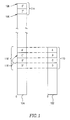
- an original reserved memory 110 which is part of an original system memory 102, is shown.
- the original reserved memory 110 comprises address locations which are grouped together for purposes of discussion into portions A-D. In one embodiment, these portions represent arbitrary subdivisions (that is, of no particular size) into which system subroutines or reserved storage locations can reside.
- FIG. 1 Also shown in Figure 1 is a new system memory 104 having within it certain memory locations corresponding to the address locations of the original reserved memory 110. These corresponding memory locations are referred to collectively as a shadow memory, which are indicated by 110'. The address locations encompassed by original reserved memory 110 and the shadow memory 110' are not accessible by typical software applications for general storage purposes.
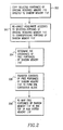
- a block 202 describes the first step in the memory management operation, which states that selected portions of original reserved memory 110 are to be copied "directly" from the original reserved memory 102 to the corresponding portions of the new system memory 104.
- a processing unit such as a central processing unit (CPU) of the microcomputer (not shown) to corresponding portions of shadow memory 110' without the use of any intermediate memory locations.
- CPU central processing unit
- shadow memory 110' without the use of any intermediate memory locations.
- a block 203 shows the next step of causing any accesses to the selected portions of the original reserved memory 110 to be re-directed to the corresponding portions of the shadow memory 110'
- any subsequent read or write accesses to a memory location within the portion designated A are redirected to the corresponding location at A'.
- This block 204 indicates that a determination must be made as to which portions of shadow memory 110' are unused, and thus free.
- This unused memory results from not selecting portions of original reserved memory 110 to be shadowed. For example, if the portion of reserved memory designated D ( Figure 1) has not been selected to be shadowed, then the corresponding portion of shadow memory designated D' will remain unused.
- a block 206 contents of those portions of shadow memory 110' which are utilized (that is, which store the contents of a selected portion of original reserved memory 110) are copied to portions of shadow memory 110' contiguous with other utilized portions of shadow memory 110'. In this way, utilized portions of shadow memory 110' are contiguous, as are the portions of free reserved memory.
- FIG. 1 An example of the above is shown by Figure 1, which shows that portions A' and C' of the shadow memory 110' are utilized by the system, and blocks B and D are not. As shown diagrammatically by an arrow 116, the contents of portion C' are then transferred to portion B', and thus in effect the two portions B' and C' are switched. In this way, utilized portions A' and C' are contiguous in shadow memory 110', as are portions B' and D' which contain the free reserved memory.
- FIG. 1 shows the example where free reserved memory portions B' and D' are re-mapped from the memory locations of new user memory designated by portions B'' and D'', creating the appearance of an additional system memory 114.
- the additional system memory 114 begins at the memory location shown by the highest distinct physical address of new system memory 106 and ends at the address at the top of the re-mapped portion 108.
- memory portions C' and D' appear to have been physically moved to the memory locations beginning at the highest distinct physical address of new system memory 106.
- the memory addresses corresponding to the additional system memory 114 appear to the software application (not shown) to be usable, accessible memory locations.
- the additional system memory 114 has been re-mapped to the free reserved memory within shadow memory 110'.
- This re-mapping then allows a typical software application to utilize free reserved memory that would otherwise not be accessible. It should be emphasized, however, that no additional physical memory is actually associated with additional system memory 114. It only appears that way to a typical software application.
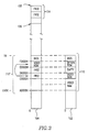
- Figure 3 shows a preferred embodiment of the anticipated contents of original reserved memory 110. These contents include a BIOS, option ROM, video ROM and video RAM. It should be understood that the contents of original reserved memory 110 as shown in Figure 3 only relate to a preferred embodiment, and that other items (such as memory files) can also be part of original reserved memory 110.
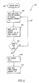
- Figure 4 shows diagrammatically a preferred embodiment for shadowing selected portions of original reserved memory 110 during initialization of the microcomputer (not shown).
- the original reserved memory 110 is partitioned into portions of equal length. Each of these portions has associated with it a bit, called a shadow bit, preferably stored in a register (not shown). Each shadow bit controls the shadowing for each of the portions of the original system memory 110 when selected, as described below.
- the shadow bits are reset to 0 (as shown by oval 401), and an address pointer (not shown) is set to the first memory location of a selected portion of original reserved memory 110. Then, beginning with a block 402, a double word of data from a selected portion of original reserved memory 110 is read by the CPU (not shown).
- the CPU After the CPU has read the double word of data, the CPU is then instructed to write the double word of data back to the same address that it had originally read the double word of data from, as shown by a block 404.
- the present invention actually causes the double word of data to be written directly to a corresponding portion of the shadow memory 110'. It should be noted that since the original reserved memory 110 and the new reserved memory 110' have identical memory addresses, only one of these memories can be enabled and accessed at any one time. Thus, the present invention controls which of the two reserved memories (either the original reserved memory 110 or new reserved memory 110') to read from and write to. It should be understood that a CPU as used above is used only by way of example, and that other types of processing units could also be used.
- the present invention determines if there are any more words of data to be read from the selected portion of the reserved memory 110, as is shown by a decision box 406. If there is more memory to read, then the next double word of data is read from the selected portion of the original reserved memory 110, and the cycle continues until the entire selected portion of original reserved memory 110 is copied, as is shown by the loop made up of an arrow 407, block 402, block 404, and decision block 406. If there is no more memory to read, then the shadow bit is set to 1, as indicated by a block 408.
- the shadow bit is used as an indication as to which of the system memories (original system memory 102 or new system memory 104) is enabled.
- the shadow bit is merely an indication of the mode of operation of the present invention (which is explained in more detail below), and that any means for indicating such modes could also be used. It should also be understood that while the reading and writing of a double word of data was performed by the CPU, that any unit of data which the CPU (or any other processing unit such as a direct memory access controller) can load and store could also be used.
- the original reserved memory 110 and shadow memory 110' both reside at system memory locations having addresses in the range between, for example, A0000H (H meaning hexidecimal) and FFFFFH (this address range generally referred to herein as the reserved memory range). These addresses are used in a preferred embodiment since they correspond to industry standards for IBM PCs and compatibles. However, it should be understood that original reserved memory 110 and shadow memory 110' could also be at a different address, and be of different sizes.
- shadow memory 110' there may be portions of shadow memory 110' which are not being utilized, and thus could be used by typical software applications for general storage purposes should they be able to access these free reserved memory portions. Since typical software applications are generally not designed to address reserved memory 110' for general storage purposes, re-mapping of the addresses must be accomplished to make this free reserved memory accessible.
- the BIOS and video ROM are selected to be shadowed.
- all other portions of shadow memory 110' corresponding to non-selected portions of original reserved memory 110 are not utilized, and thus contain free reserved memory.
- the first step that the present invention takes is to cause the utilized and free portions of shadow memory 110' to be contiguous.
- An example of this first step is as follows. The contents of the video ROM from the portion of shadow memory 110' beginning at address C0000H, are copied to the portion beginning at address E0000H, as indicated by an arrow 402.
- those portions of shadow memory 110' corresponding to those portions of original reserved memory 110 containing the video ROM and BIOS form a contiguous portion of utilized reserved memory
- the portions of shadow memory 110' containing the option ROM and video RAM form a contiguous section of free reserved memory.
- the present invention determines the highest memory location of new system memory 104.
- This highest distinct physical address of new system memory is shown by 106 in Figure 3.
- Figure 3 shows an example where the additional system memory 114 is re-mapped to shadow memory 110' at addresses A0000H - DFFFFH. In this way, a typical software application which attempts to use memory locations from 0 to 256 kilobytes (Kbytes) above the highest distinct physical address of new system memory 106 actually is accessing free reserved memory.
- shadow memory 110' is subdivided into portions, each portion being 64 Kbytes in size. Also in a preferred embodiment, only the BIOS, option ROM, and video ROM portions of original reserved memory 110 can be shadowed. It should be understood, however, that other arrangements are possible, enabling other portions of original reserved memory 110 to be shadowed.
- the decision regarding which portions of original reserved memory are to be selected for shadowing is made by a user prior to the initialization of the microcomputer. This selection information is maintained in configuration information within a non-volatile memory, so that it is retained when the main power to the microcomputer is discontinued.
- the BIOS When the microcomputer is initialized, the BIOS reads the information in this non-volatile memory, and detects which of the portions of original reserved memory 110 have been selected to be shadowed.
- a shadow bit located in an I/O register 508 (as will be shown in Figure 5 below), is used to determine the mode of operation, or state of the shadowing mechanism for a selected portion of the original reserved memory 110.
- this shadow bit is reset to 0.
- the shadow bit being 0 indicates that memory is read from original reserved memory 110 and written to shadow memory 110'.
- any read accesses to a memory location within the reserved memory range will result in the memory within the original reserved memory 110 being read from.
- an attempt to write to a memory location within the reserved memory range will result in the memory within the shadow memory 110' being written to.
- this shadow memory 110' is a form of DRAM.
- the shadow bits 520 in I/O register 508 are reset to 0 during initialization of the microcomputer.
- the BIOS 524 then directs the CPU to read a double word of data at an address of a selected portion of original reserved memory 110 that is to be shadowed.
- An inhibit circuit 512 receives this address via address line 510.
- the inhibit circuit receives signals via a read/write line 504 indicating whether a read or a write cycle is occurring.
- a 0 from the BIOS 524 over read/write line 504 indicates that a read cycle is occurring, and a 1 indicates that a write cycle is occurring.
- the inhibit circuit 512 determines that the address to be read from is that from original reserved memory 110, as opposed to shadow memory 110'. Then, the inhibit circuit 512 sends a 1 over a disable line 514 to a logic circuit 516. As a result, the logic circuit 516 sends a 1 over chip enable line 518, disabling system memory. Also, the logic circuit 516 sends a 0 over host local memory signal line 520, which enables the original system memory 102. Thus, the data which is read is read from the original reserved memory 110 on the original system memory 102.
- the BIOS 524 then directs the CPU to write the double word of data back to the same address as it was read from.
- Inhibit circuit 512 upon receiving a 0 from the BIOS via read/write line 504 indicating that a write cycle is occurring, and noting that the shadow bits 520 in I/O register 508 are 0, sends a 0 over disable line 514 to logic circuit 516.
- Logic circuit then sends a 0 over chip enable line 518 to enable new system memory 104, and sends a 1 over host local memory signal line 520 to disable original system memory 102.
- the BIOS 524 writes to the memory location at from which it previously read, it is actually writing to the shadow memory 110' on new system memory 104.
- BIOS 524 sends information to I/O register 508 via I/O port 522, specifying which portions of original reserved memory 110 have been copied to new reserved memory 110'.
- the shadow bits 520 within the I/O register 508 representing portions of original reserved memory 110 which have been copied to shadow memory 110' are then set equal to 1.
- the inhibit circuit 512 On subsequent read cycles, the inhibit circuit 512 will receive the address via address line 510 of the memory location to be read. The inhibit circuit 512 is only sensitive to addresses within the reserved memory range. If the bits in I/O register 508 indicate to the I/O register 508 that the address is to a portion of original reserved memory 110 which had been selected to be shadowed, the inhibit circuit sends a 0 over disable line 514 to logic circuit 516, which enables shadow memory 110' and disables original reserved memory 110 as described above. Thus, the read will occur from shadow memory 110'. If the address has not been from a selected portion of original reserved memory 110, the read will occur from the original reserved memory 110 itself.
- logic circuit 516 On subsequent write cycles, if the address to be written is within the reserved memory range and if the inhibit circuit 512 notes that the address is within a portion of original reserved memory which had been selected to be shadowed, then logic circuit 516 will disable both the shadow memory 110' and the original reserved memory 110. Thus, logic circuit 516 sends a 1 over chip enable line 518, and a 1 over host local memory signal line 520. In this way, the shadow memory 110' is effectively write-protected at this point.
- only three specified portions of original reserved memory 110 are permitted to be shadowed. Specifically, these three portions are each 64 Kbytes in size, and begin at C0000 H (video ROM), E0000H (option ROM) and F0000H (BIOS). It should be understood that the present invention contemplates the use of a shadowing mechanism which is not limited to shadowing the specific above-noted three portions of original reserved memory 110, and is also not limited to shadowing exactly three portions of original reserved memory 110. It should also be understood that the above-noted portions of original reserved memory 110 could be of any size, and are not limited to 64 Kbytes.
- the above-noted shadowing technique consequently allows portions of the original reserved memory 110 to be efficiently and selectively copied to a shadow memory 110' which is typically faster than the original reserved memory 110. Since portions of the original reserved memory 110 such as the BIOS are frequently accessed, such shadowing enables the microcomputer as a whole to operate more quickly.
- re-mapping entails taking unused portions of the shadow memory 110 (that is, free reserved memory), and re-mapping accessible memory locations to these unused portions, so that the unused portions of shadow memory 110' are accessible to typical software applications.
- re-mapping is automatically accomplished by the BIOS during the initialization of the microcomputer.
- the non-volatile memory used for designating which portions of original system memory 110 are to be shadowed is read by the BIOS, and a those portions to be re-mapped to are determined. It should be noted that those portions of shadow memory 110' which have been shadowed are not re-mapped to, since those shadowed portions of shadow memory 110' are utilized.
- the BIOS detects this, and automatically re-maps to only portions A0000H-BFFFFH. It should be understood, however, that there is no inherent constraint on which portions of shadow memory 110' can be re-mapped to, nor on the number or size of such portions.
- BIOS 524 reads the non-volatile memory containing information regarding which portions of original reserved memory 110 have been selected to be shadowed, and from that determines which portions of shadow memory 110' are to be re-mapped to. BIOS 524 sends this information to I/O port 602, which passes the information through line 604 to re-map register 608.
- re-map register 608 contains a total of 2 re-map bits 626, indicative of which portions of the shadow memory 110' are to be re-mapped.
- the BIOS 524 also places in a top of memory register 628 the highest distinct physical address of new system memory 106. As indicated above, the additional system memory 114 which is accessible by typical software applications is to begin at this highest distinct physical address. Thus, the top of memory register 628 contains the starting location of additional system memory 114. The size of additional system memory 114 can be inferred from the settings of the re-map bits 626.
- the high bits of this address are received via a high bit line 614 into a re-map enable circuit 618.
- the re-map enable circuit 618 examines the high bits from the address originally sent via address line 610, and accesses the information in re-map register 608 indicative of the size of additional system memory 114, and the information in top of memory register 628, which determines the location of additional system memory 114. From this information, the re-map enable circuit 618 calculates whether the address received via address line 610 is part of additional system memory 114.
Landscapes
- Engineering & Computer Science (AREA)
- Theoretical Computer Science (AREA)
- Physics & Mathematics (AREA)
- General Engineering & Computer Science (AREA)
- General Physics & Mathematics (AREA)
- Memory System (AREA)
- Executing Machine-Instructions (AREA)
Applications Claiming Priority (2)
| Application Number | Priority Date | Filing Date | Title |
|---|---|---|---|
| US472057 | 1990-01-31 | ||
| US07/472,057 US5202994A (en) | 1990-01-31 | 1990-01-31 | System and method for shadowing and re-mapping reserved memory in a microcomputer |
Publications (2)
| Publication Number | Publication Date |
|---|---|
| EP0440446A2 true EP0440446A2 (de) | 1991-08-07 |
| EP0440446A3 EP0440446A3 (en) | 1992-04-22 |
Family
ID=23874031
Family Applications (1)
| Application Number | Title | Priority Date | Filing Date |
|---|---|---|---|
| EP19910300718 Withdrawn EP0440446A3 (en) | 1990-01-31 | 1991-01-30 | System and method for shadowing and re-mapping reserved memory in a microcomputer |
Country Status (3)
| Country | Link |
|---|---|
| US (2) | US5202994A (de) |
| EP (1) | EP0440446A3 (de) |
| JP (1) | JPH04213131A (de) |
Cited By (2)
| Publication number | Priority date | Publication date | Assignee | Title |
|---|---|---|---|---|
| EP0567237A1 (de) * | 1992-04-24 | 1993-10-27 | International Business Machines Corporation | Verfahren und Vorrichtung zur Erhöhung der benutzbaren Speicherbereiches |
| EP1282037A1 (de) * | 2001-08-03 | 2003-02-05 | Drecq Daniel Technologies D 2 T | Echtzeitschnittstellentreiber |
Families Citing this family (33)
| Publication number | Priority date | Publication date | Assignee | Title |
|---|---|---|---|---|
| CA2003821C (en) * | 1989-04-20 | 1996-12-03 | Richard J. Molnar | Process controller single memory chip shadowing technique |
| JPH03168828A (ja) * | 1989-11-29 | 1991-07-22 | Canon Inc | 情報処理装置 |
| US5428758A (en) * | 1991-05-10 | 1995-06-27 | Unisys Corporation | Method and system for remapping memory from one physical configuration to another physical configuration |
| KR100274099B1 (ko) * | 1991-08-02 | 2001-01-15 | 비센트 비.인그라시아 | 점진적으로 프로그램가능한 비휘발성 메모리 및 이를 구비한 집적 회로와 비휘발성 메모리 프로그래밍 방법 |
| US5603011A (en) * | 1992-12-11 | 1997-02-11 | International Business Machines Corporation | Selective shadowing and paging in computer memory systems |
| US5574866A (en) * | 1993-04-05 | 1996-11-12 | Zenith Data Systems Corporation | Method and apparatus for providing a data write signal with a programmable duration |
| US5748922A (en) * | 1993-04-05 | 1998-05-05 | Packard Bell Nec | Method and apparatus for reading data from a write only port |
| US5687379A (en) * | 1993-04-05 | 1997-11-11 | Packard Bell Nec | Method and apparatus for preventing unauthorized access to peripheral devices |
| US5526503A (en) * | 1993-10-06 | 1996-06-11 | Ast Research, Inc. | Virtual addressing buffer circuit |
| JP2931749B2 (ja) * | 1993-12-08 | 1999-08-09 | 株式会社東芝 | データ記録再生装置とサーボ処理方法 |
| JPH07210395A (ja) * | 1994-01-10 | 1995-08-11 | Fujitsu Ltd | ファームウェアメンテナンス方式 |
| US6421776B1 (en) * | 1994-10-14 | 2002-07-16 | International Business Machines Corporation | Data processor having BIOS packing compression/decompression architecture |
| US5692187A (en) * | 1995-02-14 | 1997-11-25 | General Magic | Shadow mechanism having masterblocks for a modifiable object oriented system |
| US5819306A (en) * | 1995-02-14 | 1998-10-06 | General Magic | Shadow mechanism for a modifiable object oriented system |
| US6125435A (en) * | 1995-09-13 | 2000-09-26 | Lexar Media, Inc. | Alignment of cluster address to block addresses within a semiconductor non-volatile mass storage memory |
| US5842012A (en) * | 1996-05-15 | 1998-11-24 | Vlsi Technology, Inc. | Efficient soft reset in a personal computer |
| US6327640B1 (en) * | 1997-03-07 | 2001-12-04 | Advanced Micro Devices, Inc. | Overlapping peripheral chip select space with DRAM on a microcontroller with an integrated DRAM controller |
| US5905889A (en) | 1997-03-20 | 1999-05-18 | International Business Machines Corporation | Resource management system using next available integer from an integer pool and returning the integer thereto as the next available integer upon completion of use |
| KR100313996B1 (ko) * | 1998-01-08 | 2001-12-28 | 구자홍 | 컴퓨터시스템의바이오스데이터저장장치및방법 |
| US6219770B1 (en) * | 1998-03-23 | 2001-04-17 | Compaq Computer Corporation | Method and apparatus for managing copy on write operations in a virtual memory |
| US6876660B1 (en) * | 1999-02-16 | 2005-04-05 | Cisco Technology, Inc. | Method for implementing automatic protection switching (APS) using cell replication |
| US6282647B1 (en) * | 1999-06-02 | 2001-08-28 | Adaptec, Inc. | Method for flashing a read only memory (ROM) chip of a host adapter with updated option ROM bios code |
| US6438672B1 (en) * | 1999-06-03 | 2002-08-20 | Agere Systems Guardian Corp. | Memory aliasing method and apparatus |
| US6446139B1 (en) * | 1999-06-28 | 2002-09-03 | Adaptec, Inc. | Multiple chip single image BIOS |
| US6704840B2 (en) * | 2001-06-19 | 2004-03-09 | Intel Corporation | Computer system and method of computer initialization with caching of option BIOS |
| US6725289B1 (en) * | 2002-04-17 | 2004-04-20 | Vmware, Inc. | Transparent address remapping for high-speed I/O |
| CA2523788A1 (en) * | 2003-05-19 | 2004-12-02 | James Hardie International Finance B.V. | Building material, building system and method of installing the same |
| US7174436B1 (en) * | 2003-10-08 | 2007-02-06 | Nvidia Corporation | Method and system for maintaining shadow copies of data using a shadow mask bit |
| US7516291B2 (en) | 2005-11-21 | 2009-04-07 | Red Hat, Inc. | Cooperative mechanism for efficient application memory allocation |
| US7555641B2 (en) * | 2006-03-20 | 2009-06-30 | Intel Corporation | Efficient resource mapping beyond installed memory space by analysis of boot target |
| CN101819518B (zh) * | 2009-02-26 | 2013-09-11 | 国际商业机器公司 | 在事务内存中快速保存上下文的方法和装置 |
| US10019193B2 (en) * | 2015-11-04 | 2018-07-10 | Hewlett Packard Enterprise Development Lp | Checkpointing a journal by virtualization of non-volatile random access memory |
| CN117573583A (zh) * | 2024-01-12 | 2024-02-20 | 上海励驰半导体有限公司 | 数据处理方法、装置、芯片及交通设备 |
Family Cites Families (8)
| Publication number | Priority date | Publication date | Assignee | Title |
|---|---|---|---|---|
| IT1020819B (it) * | 1974-09-18 | 1977-12-30 | Olivetti & Co Spa | Macchina contabile a configurazione variabile |
| US4475176A (en) * | 1981-08-06 | 1984-10-02 | Tokyo Shibaura Denki Kabushiki Kaisha | Memory control system |
| US4459658A (en) * | 1982-02-26 | 1984-07-10 | Bell Telephone Laboratories Incorporated | Technique for enabling operation of a computer system with a consistent state of a linked list data structure after a main memory failure |
| NZ209664A (en) * | 1983-09-29 | 1987-05-29 | Tandem Computers Inc | Memory board address assignments: automatic reconfiguration |
| US4564922A (en) * | 1983-10-14 | 1986-01-14 | Pitney Bowes Inc. | Postage meter with power-failure resistant memory |
| US4713756A (en) * | 1985-02-28 | 1987-12-15 | Westinghouse Electric Corp. | Non-volatile memory device for a programmable controller |
| JPH0223440A (ja) * | 1988-07-13 | 1990-01-25 | Toshiba Corp | パーソナルコンピュータ |
| US5237669A (en) * | 1991-07-15 | 1993-08-17 | Quarterdeck Office Systems, Inc. | Memory management method |
-
1990
- 1990-01-31 US US07/472,057 patent/US5202994A/en not_active Expired - Lifetime
-
1991
- 1991-01-30 EP EP19910300718 patent/EP0440446A3/en not_active Withdrawn
- 1991-01-31 JP JP3010792A patent/JPH04213131A/ja active Pending
-
1992
- 1992-09-25 US US07/951,650 patent/US5301328A/en not_active Expired - Lifetime
Cited By (3)
| Publication number | Priority date | Publication date | Assignee | Title |
|---|---|---|---|---|
| EP0567237A1 (de) * | 1992-04-24 | 1993-10-27 | International Business Machines Corporation | Verfahren und Vorrichtung zur Erhöhung der benutzbaren Speicherbereiches |
| EP1282037A1 (de) * | 2001-08-03 | 2003-02-05 | Drecq Daniel Technologies D 2 T | Echtzeitschnittstellentreiber |
| WO2003014922A3 (fr) * | 2001-08-03 | 2004-02-26 | Drecq Daniel Technologies D 2 | Programme informatique de pilotage d'interface en temps reel |
Also Published As
| Publication number | Publication date |
|---|---|
| JPH04213131A (ja) | 1992-08-04 |
| EP0440446A3 (en) | 1992-04-22 |
| US5202994A (en) | 1993-04-13 |
| US5301328A (en) | 1994-04-05 |
Similar Documents
| Publication | Publication Date | Title |
|---|---|---|
| US5202994A (en) | System and method for shadowing and re-mapping reserved memory in a microcomputer | |
| US6542971B1 (en) | Memory access system and method employing an auxiliary buffer | |
| US7519754B2 (en) | Hard disk drive cache memory and playback device | |
| US4500954A (en) | Cache bypass system with post-block transfer directory examinations for updating cache and/or maintaining bypass | |
| KR100563222B1 (ko) | 메모리 액세스 보호 | |
| US7613870B2 (en) | Efficient memory usage in systems including volatile and high-density memories | |
| EP1804156A2 (de) | Gemeinsamer Speicher und Steuerung | |
| US5906000A (en) | Computer with a cache controller and cache memory with a priority table and priority levels | |
| EP0544252A2 (de) | Datenverwaltungssystem für Halbleiterspeicher mit beschränkter Programmierung und I.C.-Speicherkarte mit solchem Datenverwaltungssystem | |
| US20050182893A1 (en) | Controller for controlling nonvolatile memory | |
| US6282644B1 (en) | Apparatus and method for storing BIOS data of computer system | |
| US20080010418A1 (en) | Method for Accessing a Non-Volatile Memory via a Volatile Memory Interface | |
| US20080010420A1 (en) | Method for Accessing Control Registers via a Memory Device | |
| JPH10207768A (ja) | エンジン動作中におけるフラッシュ・メモリにアクセスするための方法および装置 | |
| US20080010419A1 (en) | System and Method for Issuing Commands | |
| US6738887B2 (en) | Method and system for concurrent updating of a microcontroller's program memory | |
| JPH07114500A (ja) | 不揮発性メモリ記憶装置 | |
| US20080016296A1 (en) | Data processing system | |
| US20080007569A1 (en) | Control protocol and signaling in a new memory architecture | |
| US5873128A (en) | Data processing system with dynamic address translation function | |
| JPH04133117A (ja) | 情報処理装置 | |
| JPS5924428B2 (ja) | 表示装置 | |
| JPH0520196A (ja) | デイスク・キヤツシユ制御装置 | |
| JPH0210446A (ja) | バッファ記憶装置 | |
| JP4724289B2 (ja) | データ処理装置およびデータ処理装置のメモリアクセス制御方法 |
Legal Events
| Date | Code | Title | Description |
|---|---|---|---|
| PUAI | Public reference made under article 153(3) epc to a published international application that has entered the european phase |
Free format text: ORIGINAL CODE: 0009012 |
|
| AK | Designated contracting states |
Kind code of ref document: A2 Designated state(s): DE FR GB IT |
|
| PUAL | Search report despatched |
Free format text: ORIGINAL CODE: 0009013 |
|
| AK | Designated contracting states |
Kind code of ref document: A3 Designated state(s): DE FR GB IT |
|
| 17P | Request for examination filed |
Effective date: 19920818 |
|
| 17Q | First examination report despatched |
Effective date: 19950412 |
|
| STAA | Information on the status of an ep patent application or granted ep patent |
Free format text: STATUS: THE APPLICATION IS DEEMED TO BE WITHDRAWN |
|
| 18D | Application deemed to be withdrawn |
Effective date: 19951024 |