EP0441533A2 - Appareil pour le triage et stockage de données - Google Patents
Appareil pour le triage et stockage de données Download PDFInfo
- Publication number
- EP0441533A2 EP0441533A2 EP91300775A EP91300775A EP0441533A2 EP 0441533 A2 EP0441533 A2 EP 0441533A2 EP 91300775 A EP91300775 A EP 91300775A EP 91300775 A EP91300775 A EP 91300775A EP 0441533 A2 EP0441533 A2 EP 0441533A2
- Authority
- EP
- European Patent Office
- Prior art keywords
- magnitude
- register
- registers
- data
- data word
- Prior art date
- Legal status (The legal status is an assumption and is not a legal conclusion. Google has not performed a legal analysis and makes no representation as to the accuracy of the status listed.)
- Withdrawn
Links
Images


Classifications
-
- G—PHYSICS
- G06—COMPUTING OR CALCULATING; COUNTING
- G06F—ELECTRIC DIGITAL DATA PROCESSING
- G06F7/00—Methods or arrangements for processing data by operating upon the order or content of the data handled
- G06F7/22—Arrangements for sorting or merging computer data on continuous record carriers, e.g. tape, drum, disc
- G06F7/24—Sorting, i.e. extracting data from one or more carriers, rearranging the data in numerical or other ordered sequence, and rerecording the sorted data on the original carrier or on a different carrier or set of carriers sorting methods in general
Definitions
- the present invention relates generally to the field of computer memory and storage devices. More particularly, the present invention is directed to a self-sorting storage device that automatically inserts incoming data words between words of lesser and greater magnitude in a manner that stores the data in rank order.
- Stack a dedicated area of memory known as a "stack”, or “pushdown stack”, which is particularly useful for quickly storing and retrieving data.
- Data is generally written to and read from the stack with simple one-word statements. For example, "PUSH A” is a typical command for loading the contents of Register “A” onto the stack. Similarly, “POP A” would result in the data word located at the top of the stack being loaded into Register A.
- Stack data can generally be accessed faster, e.g., in a single clock cycle, than data stored in other areas of memory.
- FIFO first-in-first-out
- LIFO last-in-first-out
- apparatus for sorting and storing incoming data words according to their magnitudes comprises: means, such as a sequence of registers, for storing a sequence of data words; and sorting means coupled to the registers for receiving incoming data words and loading them into the registers in rank order in accordance with their magnitudes.
- the stored data words are maintained in sequential locations (or registers, if a stack of registers is used) with lesser values preceding greater values.
- the stored data words are maintained in sequential locations with greater values preceding lesser values.
- the means for storing the data words comprises a stack of a fixed number (e.g. eight) of registers.
- the sorting means comprises means for comparing the magnitude of at least one stored data word with the magnitude of the incoming data word, and for providing an output signal indicative of whether the incoming data word is less than the stored data word.
- the most preferred embodiment further comprises control means, coupled to the comparator and sorting means, for providing a control signal to the sorting means; and means (such as a plurality of multiplexers) responsive to the control signal, for storing the incoming data word in the sequence in rank order. Derivation of the control signal is dependent upon the comparator output signals and an externally generated mode signal.
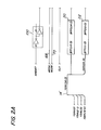
- Figure 1 is a simplified block diagram of a self-sorting storage device according to the present invention.
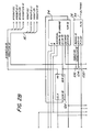
- FIGS. 2A - 2F are a detailed schematic diagram of a self-sorting stack embodying the present invention.
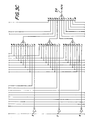
- Figures 3A - 3E are a schematic diagram of a preferred comparator circuit for use in the self-sorting stack of Figure 2.
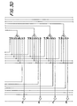
- Figure 4 is a diagram illustrating one embodiment of pin connections of a preferred controller for use in the self-sorting stack of Figure 2.
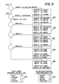
- Figure 5 is a flowchart of a preferred operation for operating the controller of Figure 4.
- the invention broadly comprises means for receiving incoming data words and storing the incoming words in rank order according to their magnitudes.
- the means for storing the data preferably comprises data registers, but may also include other types of storage devices, for example, RAM, bubble memory, etc. It is the means and method by which the data is automatically sorted that forms the basis of the instant invention.
- FIG. 1 there is illustrated a simplified block diagram of a sorting device according to the present invention.
- Figure 1 is merely a broad representation of the invention.
- the sorting device comprises sorting means 10 for receiving incoming data words on a line 14 and outputting those words to a plurality of storage devices (e.g. registers) 12a, 12b, 12c, 12d etc.
- storage devices e.g. registers
- Sorting means 10 is capable of accessing the storage devices in a parallel fashion so that an incoming data word can be stored within any register, depending upon the value, or magnitude, of the data word being stored. In this way, the stored data is maintained in rank order.
- data is maintained in a "stack" of data registers in increasing order, although with a few obvious modifications the data may be maintained in decreasing order.
- a sorting device that sorts and stores the data in decreasing order is therefore contemplated as being within the scope of the invention.
- the self-sorting stack illustrated in Figure 2 comprises a plurality of fifteen bit wide four-to-one multiplexers 24, 28, 32, 36, 40, 44, 48, 52; a plurality of fifteen bit registers 12a', 12b', 12c', 12d', 12e', 12f', 12g', 12h'; and a plurality of twelve bit comparators 26, 30, 34, 38, 42, 46 and 50.
- Multiplexers 24, 28, 32, 36, 40, 44, 48, 52 are controlled by controller 110 (not shown in Fig. 2). Controller 110 is discussed below in connection with Figure 4. Though the invention is described herein for sorting fifteen bit data words, it should be understood that this represents merely one implementation of the invention, and that the invention is not so limited.
- Incoming data words are received on line 14'.
- Each data word comprises fifteen bits of digital data and is received by buffers 20 and 22.
- Buffer 20 receives all fifteen bits of the incoming words on line 14' and transmits the word to the "D3" input of multiplexers 24, 28, 32, etc.
- Buffer 22 receives twelve bits of the incoming word on line 14' and outputs these twelve bits to the "P" inputs of comparators 26, 30, 34, 38, 42, 46, 50.
- multiplexer 24, 28, 32, 36, 40, 44, 48, 52 associated with each of the storage registers 12a', 12b', 12c', 12d', 12e', 12f', 12g', 12h' respectively; and there are four data input terminals, "D0", "D1", “D2" and "D3" respectively, for each multiplexer.
- the D3 inputs receive new data from buffer 20.
- the D2 inputs except for the last multiplexer in the sequence 52, receive data from the register immediately below (e.g. D2 of multiplexer 24 receives data from register 12b').
- the D inputs receive data from their associated registers (e.g. D1 of multiplexer 24 receives data from register 12a').
- the D0 input of each multiplexer except for the first multiplexer in the sequence 24, receives data from the register immediately above (e.g. D0 of multiplexer 28 receives data from register 12a').
- the D0 input of multiplexer 24 and the D2 input of multiplexer 52 are grounded.
- each multiplexer 24, 28, 32 etc. The basic function of each multiplexer 24, 28, 32 etc. is to control whether its associated register (i) receives new, or "incoming", data, (ii) receives data from the register immediately above or below it, or (3) remains unchanged.
- Control logic for controlling the multiplexers is contained in controller 110, which is described below with reference to Figures 4 and 5.
- Control lines for each multiplexer designated 68, 70 for multiplexer 24; 72, 74, for multiplexer 28; etc., are coupled to controller 110.
- the controller 110 provides control signals to the "A" and "B" inputs of each multiplexer. The control logic is discussed below with reference to Figures 4 and 5.
- Each comparator 26, 30, 34 etc. receives new data on its "P” input (or terminal), and data from its associated register on its “Q” input. For example, referring to comparator 26, its P input is driven by buffer 22 over line 102, and its Q input is driven by its associated register 12a' over line 104.
- the output signal of each comparator designated “PLTQ” is TRUE when the magnitude of P is less than the magnitude of Q, and false otherwise.
- the PLTQ signal of each comparator is input to controller 110 ( Figure 4) over lines 54, 56, 58, 60, etc. Each PLTQ signal is transmitted to a different input terminal, designated "CMPLT0", “CMPLT1", “CMPLT2” etc. respectively, of controller 110.
- Each comparator also has an input entitled "REGVALID” which receives bit zero of the data word stored in its associated register. Bit zero is the "valid bit” of the data, and, when zero, indicates that the associated register is empty. When the valid bit of a data word in a register is zero, or FALSE, then the output signal of its associated comparator is forced TRUE, which indicates to controller 110 that the incoming data is less in magnitude than the current contents of the register. By setting the comparator in this manner, the magnitude of an incoming data word is defined as being less than data words whose valid bit is FALSE, indicating an empty register. Empty registers are thus kept at the bottom of the stack.
- Each of the multiplexers 24, 28, 32 etc. also has an input designated "NZEROVAL".
- NZEROVAL of a particular multiplexer is FALSE
- the "valid bit" of the data word in that multiplexer's associated register is forced FALSE, indicating that the associated register is empty.
- the NZEROVAL inputs are driven by reset circuitry 100. When actuated, reset circuitry 100 therefore clears bit zero of registers 12a', 12b', 12c', etc.
- Line 16' Data is retrieved from registers 12a', 12b', 12c' etc. via line 16'.
- line 16' preferrably comprises one conductor for each bit of the data word being retrieved.
- data words are taken from the first register in the sequence, i.e. 12a', and subsequent data words are "pushed up" in the stack. This operation is automatically performed by multiplexers 24, 28, 32 etc. under the direction of controller 110.
- controller 110 To fully appreciate the operation of the preferred embodiment, one should have an understanding of the control logic. The controller and control logic are discussed with reference to figures 4 and 5 below. This discussion, however, will be preceded by a very brief discussion of preferred circuitry for implementing comparators 26, 30, 34, 38, 42, 46 and 50.
- FIG. 3 therein is depicted preferred comparator circuitry for use in the self-sorting stack of Fig. 2.
- circuitry of Fig. 3 will be discussed with reference to comparator 26, although in fact the same circuitry is employed in all of the comparators.
- the P, Q, and REGVALID inputs to comparator 26 are provided over lines 102, 104, and 106 respectively.
- the circuitry shown is a combinatorial logic circuit whereby comparisons are performed in parallel. Note that no comparison is made for the contents of the last register in the sequence, i.e. register 12h', since if the new data word is not less than the contents of any of the preceding registers, then by default it is stored in the last register. Since the function of the comparators is described above with reference to Figure 2 and the circuitry shown in Figure 3 employs basic digital circuit techniques, the manner in which the circuitry operates will be apparent to those skilled in the art. Further discussion of Figure 3 is therefore unnecessary.
- CMPLT0 inputs to the controller, designated "CMPLT0”, “CMPLT1”, “CMPLT2”, “CMPLT3”, “CMPLT4", “CMPLT5" and “CMPLT6"
- CMPLT0 inputs to the controller
- MODE inputs to the controller
- the input designated “MODE” is provided over line 112 by an external source. The external source is not considered part of the invention.
- the MODE signal comprises two bits, the function of which will be discussed with reference to Fig. 5.
- controller 110 The outputs of controller 110 are designated "MUX0[0]", “MUX0[1]”, “MUX1[0]”, “MUX1[1]”, “MUX2[0]”, “MUX2[1]", “MUX3[0]”, “MUX3[1]”, “MUX4[0]”, “MUX4[1]”, “MUX5[0]”, “MUX5[1]”, “MUX6[0]”, and "MUX6[1]”.
- These outputs drive the A & B inputs of the multiplexers. For example MUX0[0] is transmitted over line 68 to input A of multiplexer 24; similarly MUX0[1] is transmitted over line 70 to input B of multiplexer 24.
- the controller is a combinatorial circuit. It is the responsibility of the external source using the invention to properly apply or receive data and apply the corresponding MODE before asserting a clock signal CLK (Fig. 2A) that causes the data transfer desired.
- MODE IDLE, UNUSED .
- a determination is made of whether MODE IDLE or UNUSED. If so, the two bits of MUX0 (i.e., MUX0[0] and MUX0[1]), MUX1, MUX2, MUX3 etc. to MUX 7 are set to SAME, or "1", block 126. As discussed above, these outputs drive the A & B terminals of multiplexers 24, 28, 32 etc.
- MUX0[0] and MUX0[1] drive inputs A and B, respectively, of multiplexer 24; MUX1[0] and MUX1[1] drive inputs A and B respectively of multiplexer 28; MUX2[0] and MUX2[1] drive inputs A and B of multiplexer 32; and so on.
- MODE LOAD . If the mode selected is LOAD, new data will be inserted into the stack at a location dependent upon the various outputs of comparators 26, 30, 34, 38, 42, 46 and 50.
- the CMPLT0 input of controller 110 is tested to determine whether it is "1" (or TRUE). If TRUE, this indicates that the magnitude of the incoming data is less than the magnitude of the data word stored in first register 12a'. In this case, as shown at block 130, the two bits of MUX0 are set equal to NEWDATA (i.e. "3") and the remaining outputs (MUX1, MUX2, MUX3, MUX4, MUX5, MUX6 and MUX7) are set to ABOVE (i.e. "1").
- CMPLT0 is not TRUE
- CMPLT1 is not TRUE, similar steps are executed to determine where in the stack the incoming data should be located. If none of controller 110's inputs (i.e. CMPLT0 - CMPLT6) are TRUE, by default the incoming data is directed to the last register in the sequence, register 12h'. This is indicated at block 136 where MUX0 through MUX6 are all set to SAME and MUX7 is set to NEWDATA.
- UNLOAD UNLOAD .
- the UNLOAD procedure is represented at block 138.
- the data word in register 12a' is removed and the contents of all subsequent registers (12b'-12h') are pushed up to the immediately preceding register in the sequence.
- the last register in the sequence having valid data will automatically have its valid bit set to show an empty register.
- these registers will be shown as empty, making a reset between uses of the stack unnecessary.
- controller 110 is a combinatorial circuit.
- the following are logic equations describing a preferred implementation of the controller 110 and correspond to the flowchart of Figure 5.
- the operation of the self-sorting stack just described may be summarized as follows: The eight registers of the stack are cleared, showing that their respective entries are not valid. When a new data word is to be loaded in the stack, it is simultaneously compared to the contents of each of the eight registers. If the first word is invalid, then the data is inserted in the first register. If the first word is valid, a determination is made as to whether it is less than the incoming data. If it is, then the existing data in the stack is pushed down one register and the new data is inserted in the first register. If the new data is not less than the data in the first register, it is compared to the data in the second register using the same procedure and results, and so on, through all eight registers. The new data word will therefore only be inserted after data of lesser magnitude. All comparisons are made in one clock cycle.
- the preferred embodiment is implemented with a plurality of multiplexers, registers, and associated comparators, and a single controller for controlling the multiplexers. All of this may be integrated into a single device using known integrated circuit technology.
Landscapes
- Engineering & Computer Science (AREA)
- General Engineering & Computer Science (AREA)
- Theoretical Computer Science (AREA)
- Computer Hardware Design (AREA)
- Physics & Mathematics (AREA)
- General Physics & Mathematics (AREA)
- Time-Division Multiplex Systems (AREA)
- Information Retrieval, Db Structures And Fs Structures Therefor (AREA)
- Executing Machine-Instructions (AREA)
Applications Claiming Priority (2)
| Application Number | Priority Date | Filing Date | Title |
|---|---|---|---|
| US07/478,126 US5222243A (en) | 1990-02-09 | 1990-02-09 | Sorting apparatus having plurality of registers with associated multiplexers and comparators for concurrently sorting and storing incoming data according to magnitude |
| US478126 | 1990-02-09 |
Publications (2)
| Publication Number | Publication Date |
|---|---|
| EP0441533A2 true EP0441533A2 (fr) | 1991-08-14 |
| EP0441533A3 EP0441533A3 (en) | 1993-01-07 |
Family
ID=23898635
Family Applications (1)
| Application Number | Title | Priority Date | Filing Date |
|---|---|---|---|
| EP19910300775 Withdrawn EP0441533A3 (en) | 1990-02-09 | 1991-01-31 | Apparatus for sorting and storing data |
Country Status (3)
| Country | Link |
|---|---|
| US (1) | US5222243A (fr) |
| EP (1) | EP0441533A3 (fr) |
| JP (1) | JPH04213722A (fr) |
Cited By (3)
| Publication number | Priority date | Publication date | Assignee | Title |
|---|---|---|---|---|
| WO1995025302A1 (fr) * | 1994-03-17 | 1995-09-21 | Michael Colin Parsons | Processeur de donnees utilise pour selectionner des elements de donnees possedant les valeurs de grandeur les plus elevees et les stocker en ordre croissant |
| EP1459466A4 (fr) * | 2001-12-27 | 2005-01-26 | Interdigital Tech Corp | Trieur d'insertion |
| EP1482403A3 (fr) * | 2003-05-29 | 2007-03-21 | Ericsson AB | Table autotriante à plusieurs clés |
Families Citing this family (4)
| Publication number | Priority date | Publication date | Assignee | Title |
|---|---|---|---|---|
| US5303381A (en) * | 1990-07-19 | 1994-04-12 | Canon Kabushiki Kaisha | Method and apparatus for sorting sequential input signals by concurrently comparing successive input signals among signals in first and second memory sections |
| US5410719A (en) * | 1992-05-27 | 1995-04-25 | Hewlett-Packard Company | Field compositor for merging data and including cells each receiving three control and two data inputs and generating one control and one data output therefrom |
| US20070233868A1 (en) * | 2006-03-31 | 2007-10-04 | Tyrrell John C | System and method for intelligent provisioning of storage across a plurality of storage systems |
| US12210371B2 (en) * | 2023-02-22 | 2025-01-28 | L3Harris Technologies, Inc. | Single-clock insertion sort scheme |
Family Cites Families (12)
| Publication number | Priority date | Publication date | Assignee | Title |
|---|---|---|---|---|
| US3931612A (en) * | 1974-05-10 | 1976-01-06 | Triad Systems Corporation | Sort apparatus and data processing system |
| NL8006163A (nl) * | 1980-11-12 | 1982-06-01 | Philips Nv | Inrichting voor het sorteren van datawoorden volgens de waarden van telkens daarbij behorende attribuutgetallen. |
| US4628483A (en) * | 1982-06-03 | 1986-12-09 | Nelson Raymond J | One level sorting network |
| NL8203844A (nl) * | 1982-10-04 | 1984-05-01 | Philips Nv | Geintegreerde, als bouwsteen uitgevoerde sorteerinrichting voor datawoorden en geintegreerde, dataverwerkende, processor voorzien van zo een meegeintegreerde sorteerinrichting. |
| US4567572A (en) * | 1983-02-22 | 1986-01-28 | The United States Of America As Represented By The Director Of The National Security Agency | Fast parallel sorting processor |
| JPS59229643A (ja) * | 1983-06-13 | 1984-12-24 | Fujitsu Ltd | ソ−ト演算回路 |
| DE3322706A1 (de) * | 1983-06-24 | 1985-01-10 | Fa. Carl Zeiss, 7920 Heidenheim | Schaltungsanordnung zur schnellen rangordnungsauswahl oder -sortierung |
| US4833655A (en) * | 1985-06-28 | 1989-05-23 | Wang Laboratories, Inc. | FIFO memory with decreased fall-through delay |
| EP0271626B1 (fr) * | 1986-12-16 | 1992-03-04 | International Business Machines Corporation | Mécanisme de contournement pour des unités connectées en "daisy chain" |
| US5068822A (en) * | 1988-03-16 | 1991-11-26 | Digital Equipment Corporation | Single-stage extensible sorter for sorting data and efficiently reading out sorted data, incorporating single-bit devices |
| US4991134A (en) * | 1988-03-30 | 1991-02-05 | International Business Machines Corporation | Concurrent sorting apparatus and method using FIFO stacks |
| US4958141A (en) * | 1988-07-15 | 1990-09-18 | Hughes Aircraft Company | Real time rank ordering logic circuit |
-
1990
- 1990-02-09 US US07/478,126 patent/US5222243A/en not_active Expired - Fee Related
-
1991
- 1991-01-31 EP EP19910300775 patent/EP0441533A3/en not_active Withdrawn
- 1991-02-08 JP JP3017712A patent/JPH04213722A/ja active Pending
Cited By (4)
| Publication number | Priority date | Publication date | Assignee | Title |
|---|---|---|---|---|
| WO1995025302A1 (fr) * | 1994-03-17 | 1995-09-21 | Michael Colin Parsons | Processeur de donnees utilise pour selectionner des elements de donnees possedant les valeurs de grandeur les plus elevees et les stocker en ordre croissant |
| US5878358A (en) * | 1994-03-17 | 1999-03-02 | Mp Research Ltd. | Data processor for selecting data elements having the highest magnitude values and storing them in ascending order |
| EP1459466A4 (fr) * | 2001-12-27 | 2005-01-26 | Interdigital Tech Corp | Trieur d'insertion |
| EP1482403A3 (fr) * | 2003-05-29 | 2007-03-21 | Ericsson AB | Table autotriante à plusieurs clés |
Also Published As
| Publication number | Publication date |
|---|---|
| US5222243A (en) | 1993-06-22 |
| JPH04213722A (ja) | 1992-08-04 |
| EP0441533A3 (en) | 1993-01-07 |
Similar Documents
| Publication | Publication Date | Title |
|---|---|---|
| EP0054588B1 (fr) | Appareil interactif de recherche de données | |
| EP0312239A2 (fr) | Dispositif de commande pour un tampon "peps" par message | |
| US5805086A (en) | Method and system for compressing data that facilitates high-speed data decompression | |
| GB1563620A (en) | Multistage sorter with concurrent access to interstage buffer memories | |
| US4873667A (en) | FIFO buffer controller | |
| JPH0330898B2 (fr) | ||
| US4969164A (en) | Programmable threshold detection logic for a digital storage buffer | |
| JPH0728624A (ja) | ソート装置及びソート方法 | |
| EP0234038A2 (fr) | Appareil pour identifier le module LRU dans une mémoire | |
| US5081608A (en) | Apparatus for processing record-structured data by inserting replacement data of arbitrary length into selected data fields | |
| US4758899A (en) | Data compression control device | |
| US5222243A (en) | Sorting apparatus having plurality of registers with associated multiplexers and comparators for concurrently sorting and storing incoming data according to magnitude | |
| EP0333346A2 (fr) | Circuit de triage de données câblé | |
| US4896306A (en) | Electronic scheduler capable of searching schedule data based on time | |
| US5019969A (en) | Computer system for directly transferring vactor elements from register to register using a single instruction | |
| US4633489A (en) | Interface unit inserted between a data transfer unit and a processor unit | |
| EP0166577A2 (fr) | Appareil et procédé de tri et d'emmagasinage d'informations | |
| US4528648A (en) | Memory management system | |
| EP0227348A2 (fr) | Circuit et méthode de mémoire adressable par contenu | |
| JPH09128241A (ja) | ファジーロジックプロセッサの言語入力値の所属関数値に対する配列方法および装置 | |
| US6763422B2 (en) | Cache memory capable of reducing area occupied by data memory macro units | |
| US5732011A (en) | Digital system having high speed buffering | |
| US5161217A (en) | Buffered address stack register with parallel input registers and overflow protection | |
| JP3357243B2 (ja) | 画像処理装置における設定データ変更装置 | |
| US6671781B1 (en) | Data cache store buffer |
Legal Events
| Date | Code | Title | Description |
|---|---|---|---|
| PUAI | Public reference made under article 153(3) epc to a published international application that has entered the european phase |
Free format text: ORIGINAL CODE: 0009012 |
|
| AK | Designated contracting states |
Kind code of ref document: A2 Designated state(s): DE FR GB |
|
| PUAL | Search report despatched |
Free format text: ORIGINAL CODE: 0009013 |
|
| AK | Designated contracting states |
Kind code of ref document: A3 Designated state(s): DE FR GB |
|
| 17P | Request for examination filed |
Effective date: 19930316 |
|
| 17Q | First examination report despatched |
Effective date: 19951002 |
|
| STAA | Information on the status of an ep patent application or granted ep patent |
Free format text: STATUS: THE APPLICATION IS DEEMED TO BE WITHDRAWN |
|
| 18D | Application deemed to be withdrawn |
Effective date: 19960801 |