EP0443512B1 - Elément électrique composé ayant une structure multicouche empilée - Google Patents
Elément électrique composé ayant une structure multicouche empilée Download PDFInfo
- Publication number
- EP0443512B1 EP0443512B1 EP91102336A EP91102336A EP0443512B1 EP 0443512 B1 EP0443512 B1 EP 0443512B1 EP 91102336 A EP91102336 A EP 91102336A EP 91102336 A EP91102336 A EP 91102336A EP 0443512 B1 EP0443512 B1 EP 0443512B1
- Authority
- EP
- European Patent Office
- Prior art keywords
- coil
- conductors
- layer
- conductor
- stacked
- Prior art date
- Legal status (The legal status is an assumption and is not a legal conclusion. Google has not performed a legal analysis and makes no representation as to the accuracy of the status listed.)
- Expired - Lifetime
Links
- 239000002131 composite material Substances 0.000 title claims description 21
- 239000004020 conductor Substances 0.000 claims description 150
- 238000004804 winding Methods 0.000 claims description 42
- 239000003990 capacitor Substances 0.000 claims description 19
- 239000000696 magnetic material Substances 0.000 claims description 13
- 238000000034 method Methods 0.000 description 18
- 238000004519 manufacturing process Methods 0.000 description 7
- 230000008569 process Effects 0.000 description 6
- 238000007639 printing Methods 0.000 description 5
- 230000001747 exhibiting effect Effects 0.000 description 4
- 230000003247 decreasing effect Effects 0.000 description 3
- 230000010354 integration Effects 0.000 description 3
- 238000005245 sintering Methods 0.000 description 3
- 229910000859 α-Fe Inorganic materials 0.000 description 3
- 230000004907 flux Effects 0.000 description 2
- 238000007650 screen-printing Methods 0.000 description 2
- 239000000758 substrate Substances 0.000 description 2
- 230000009471 action Effects 0.000 description 1
- 238000000429 assembly Methods 0.000 description 1
- 230000000712 assembly Effects 0.000 description 1
- 239000011230 binding agent Substances 0.000 description 1
- 239000000919 ceramic Substances 0.000 description 1
- 229910010293 ceramic material Inorganic materials 0.000 description 1
- 230000000694 effects Effects 0.000 description 1
- 238000005516 engineering process Methods 0.000 description 1
- 230000008020 evaporation Effects 0.000 description 1
- 238000001704 evaporation Methods 0.000 description 1
- 238000003475 lamination Methods 0.000 description 1
- 239000000463 material Substances 0.000 description 1
- 230000004048 modification Effects 0.000 description 1
- 238000012986 modification Methods 0.000 description 1
- 238000000059 patterning Methods 0.000 description 1
- 230000035699 permeability Effects 0.000 description 1
- 238000000206 photolithography Methods 0.000 description 1
- 238000007747 plating Methods 0.000 description 1
- 239000002904 solvent Substances 0.000 description 1
- 238000004544 sputter deposition Methods 0.000 description 1
Images


Classifications
-
- H—ELECTRICITY
- H01—ELECTRIC ELEMENTS
- H01F—MAGNETS; INDUCTANCES; TRANSFORMERS; SELECTION OF MATERIALS FOR THEIR MAGNETIC PROPERTIES
- H01F27/00—Details of transformers or inductances, in general
- H01F27/28—Coils; Windings; Conductive connections
-
- H—ELECTRICITY
- H01—ELECTRIC ELEMENTS
- H01F—MAGNETS; INDUCTANCES; TRANSFORMERS; SELECTION OF MATERIALS FOR THEIR MAGNETIC PROPERTIES
- H01F17/00—Fixed inductances of the signal type
- H01F17/0006—Printed inductances
- H01F17/0013—Printed inductances with stacked layers
-
- H—ELECTRICITY
- H01—ELECTRIC ELEMENTS
- H01F—MAGNETS; INDUCTANCES; TRANSFORMERS; SELECTION OF MATERIALS FOR THEIR MAGNETIC PROPERTIES
- H01F17/00—Fixed inductances of the signal type
- H01F17/0006—Printed inductances
-
- H—ELECTRICITY
- H01—ELECTRIC ELEMENTS
- H01F—MAGNETS; INDUCTANCES; TRANSFORMERS; SELECTION OF MATERIALS FOR THEIR MAGNETIC PROPERTIES
- H01F17/00—Fixed inductances of the signal type
- H01F17/0006—Printed inductances
- H01F17/0013—Printed inductances with stacked layers
- H01F2017/0026—Multilayer LC-filter
Definitions
- the present invention relates generally to a composite electric part of a stacked multi-layer structure, and more particularly to an electric part of a composite structure which incorporates coils and capacitors implemented in a stacked or laminated multi-layer configuration.
- the capacitor layers can be realized in an integrated structure relatively easily by resorting to a stacked-layer capacitor manufacturing technique known heretofore.
- a stacked-layer capacitor manufacturing technique known heretofore.
- difficulty is often encountered in implementing the coil layers in an integrally stacked structure.
- the techniques which can be utilized to this end are limited, although several proposals have heretofore been made, as typified by the one disclosed in Japanese Patent Publication No. 39521/1982.
- magnetic layers of a ferrite material and electric conductors constituting a coil are stacked alternately by employing a printing process, which is then followed by sintering the stacked layer structure thus formed at a high temperature.
- a printing process which is then followed by sintering the stacked layer structure thus formed at a high temperature.
- a method is commonly adopted which comprises a step of forming by printing a film conductor of a length corresponding to about a half-turn of the coil on a substrate, a step of applying a magnetic film thereon with end portions of the conductor being exposed, and a step of printing a film conductor corresponding to the remaining half-turn on the magnetic layer in such manner that an electric connection is made to the first mentioned conductor.
- the composite electric part of the stacked multi-layer structure finds a variety of numerous applications such as for implementations of trap elements, low-pass filters, high-pass filters, band-pass filters, equalizers, IFTs and the like. Accordingly, values of capacities and inductance of the multi-layer composite electric part as well as network configuration of the capacitors and the coils has to be susceptible to selection over a wide range. In this connection, it is noted that the value and the network configuration of the capacitor can easily be adjusted over a wide range by selecting appropriately the number of the stacked layers, the number of electrodes or plates, manner of interconnection and other factors.
- the value of inductance is necessarily determined in dependence on the number of the stacked layers because of the three-dimensional structure in which the coil conductors are disposed in continuation to one another in the directions in which the layers are stacked. Accordingly, for selecting the inductance value or more particularly for increasing that value, the number of the layers has to be increased correspondingly. Consequently, as the inductance value increases, the number of the layers to be stacked is also increased correspondingly, which results in an increased overall thickness of the stacked coil structure in contradiction to the demand for a miniaturized thin structure.
- the stacked layer coil there has also been proposed such a coil structure in which a plurality of individual spiral coil conductors wound with a pitch in a same direction are embedded in axial juxtaposition within a body of a magnetic material.
- the leading end and the trailing end of each of the plural coil conductors are disposed in the same direction.
- the leading end of each coil conductor assumes a position beneath the magnetic layer, then the trailing end thereof is positioned on the top thereof. Accordingly, for connecting the coil conductors such that magnetic fields are generated in a same direction, the trailing end of the coil conductor located at the top of the magnetic layer has to be led out and connected to the leading end of the other coil conductor located at the bottom.
- JEE JOURNAL OF ELECTRONIC ENGINEERING, vol.26, no. 274, October 1989, Tokyo JP, Pages 116-118, TAKAYA: "SURFACE MOUNTING TECHNOLOGIES FOR CHIP TRANSFORMERS; FILTERS AND INDUCTORS” discloses conventional laminated transformers including two or more conductor coils stacked vertically one on the other or arranged side-by-side. Each of these transformers is simply formed by an assembly of two or more coils each of which is formed by a single conductor. Such a transformer occupies a relatively large space.
- a laminated inductor as it is also disclosed in the same document is formed by a single spirally wound conductor. Therefore the inductance which may be obtained within a predetermined space is relatively small.
- PATENT ABSTRACTS OF JAPAN vol. 13, no 207, (E-758)(3555) 16 May 1989 and corresponding JP-A-1 24407 discloses a transformer formed of two coils. Since the two coils turning in opposite directions are laterally displaced from each other, the magnetic flux is partly short-circuited, thereby reducing the net flux encircling the coils.
- a composite electric part of a stacked multi-layer structure composed of a capacitor layer and a coil layer
- the coil layer comprises at least one coil buried in a magnetic material
- said at least one coil comprises at least one combination of at least two coil conductors wound around respective winding axes extending coaxially with each other, each coil conductor being wound in a direction spirally opposite to the one of the preceding coil conductor, to which it is connected, whereby said coil conductors are mutually vertically superposed and connected mutually such that magnetic fields generated by said coil conductors are in the same direction.
- the individual coil conductors are wound spirally in the directions opposite to each other around the respective axes extending substantially coaxially, as a result of which there is realized an integrated structure in which the individual coil conductors are stacked one another at substantially same positions or locations . Consequently, the space occupied by the coil conductors and hence by the coil itself is significantly decreased. In this manner, there can be realized a composite electric part of a stacked multi-layer structure which incorporates the coil capable of exhibiting a high inductance value notwithstanding of implementation in a miniature size with a reduced thickness.
- the plurality of coil conductors include combinations each of two coil conductors wound oppositely to each other as viewed in a direction along a general winding axis, connection of the trailing end of one coil conductor to the leading end of the other coil conductor allows an electric current to flow through the coil in a same direction. Further, since the trailing end portion of one coil conductor is positioned in the same direction or orientation as the leading end portion of the other conductor, continuous connection of both coil conductors within the magnetic material can be realized extremely easily.
- the coil incorporated in the coil layer can be used not only as an inductor but also as parts of a transformer.
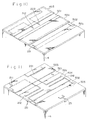
- Fig. 1 is a plan view showing, by way of example, a composite electric part of a stacked multi-layer structure according to an embodiment of the present invention and Fig. 2 is a sectional view for illustrating the stacked multi-layer structure.
- reference numeral 1 denotes generally a capacitor layer
- 2 denotes a coil layer
- reference numerals 301 to 312 denote terminal electrodes, respectively.
- the capacitor layer 1 is implemented in such a structure in which capacitor networks 11 to 13 are buried or embedded internally within a dielectric ceramic material 10.
- Each of the capacitor networks 11 to 13 is realized by interconnecting in a desired circuit configuration the individual capacitor elements each of which is formed by disposing electrodes in opposition to each other with a dielectric ceramic layer being interposed therebetween.
- the circuit configurations of the capacitor networks 11 to 13 can be selected arbitrarily by taking into account the applications for which they are intended.
- These capacitor networks 11 to 13 are connected to given ones of the terminal electrodes 301 to 312 to be led externally.
- the coil layer 2 is integrally stacked onto the capacitor layer 1 by resorting to suitable means such as sintering or bonding.
- the coil layer 2 is stacked on and over one surface of the capacitor layer 1.
- a pair of coil layers 2 may be laminated over both surfaces of the capacitor layer 1, as shown in Fig. 3.
- a pair of capacitor layers 1 are stacked on both surfaces of the coil layer 2, although not shown in the drawing.
- the coil layer 2 can be implemented in such a structure in which coils 21 to 24 are embedded or buried in a magnetic material 20 such as ferrite or the like.
- the number of the coils 21 to 24 as well as the numbers of turns thereof may arbitrarily be selected in accordance with a circuit configuration to be implemented.
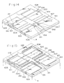
- Figs. 4 and 5 are pictorial views each illustrating in the form of a model a structure which is to be imparted to at least one of the coils 21 to 24 of Fig. 6.
- at least one of the coils 21 to 24 includes two electric coil conductors 201 and 202.
- reference numeral 203 denotes a connecting portion at which the coil conductors 201 and 202 are connected to each other and numerals 204 and 205 denote terminals, respectively.
- the coil conductors 201 and 202 are wound such that turns or windings thereof follow helical paths around respective winding axes 0, which are substantially coincident with each other (i.e. the winding axis of the coil conductor 201 extends through a space defined by the windings or turns of the coil conductor 202 and vice versa). For this reason, only a single general winding axis O is shown in the drawing.
- the winding direction a1 of the coil conductor 201 is opposite to the winding direction b1 of the coil conductor 202 as viewed in the direction in which the general winding axis O extends.
- the winding direction a1 of the coil conductor 201 is counterclockwise while the winding direction b1 of the coil conductor 202 is clockwise as viewed with reference to the direction of the general winding axis O.
- the coil conductors 201 and 202 are connected to each other by the connecting portion 203 such that magnetic fields of the same direction are generated by both the coil conductors 201 and 202 under the action of a current when it flows through these coil conductors.
- the trailing end of the coil conductor 201 and the leading end of the coil conductor 202 may be connected to each other through the connecting portion 203.
- the winding direction a1 of the coil conductor 201 is opposite to that b1 of the coil conductor 202 as viewed in the direction along the general winding axis O, there can be realized a coil structure by the coil conductors 201 and 202 in which the current flows in the same direction by connecting mutually the trailing end of the former and the leading end of the latter at the connecting portion 203.
- the terminal portions 204 and 205 are connected, respectively, to given ones of the terminal electrodes 301 to 312 shown in Figs. 1 and 2.
- inductance value L(H) of the whole coil structure or assembly is approximately four times as high as that of the coil structure formed of the single coil conductor on the assumption that the numbers n1 and n2 of turns of the coil conductors 201 and 202 are substantially equal to each other.
- both coil conductors 201 and 202 can be interconnected interiorly of the magnetic material 20 without need for leading outwardly these coil conductors 201 and 202 for the purpose of interconnection. This in turn means that the interconnecting structure for the coil conductors 201 and 202 can be much simplified with the connecting procedure being extremely facilitated.
- FIG. 5 there is shown a coil structure according to another embodiment of the invention.
- This coil structure comprises three coil conductors 200, 201 and 202 which are helically wound around respective winding axes which substantially coincide with one another. For this reason, only one general winding axis O is shown in Fig. 5.
- the winding direction a o of the coil conductor 200 is opposite to that b1 of the coil conductor 201 while the winding direction b1 of the coil conductor 201 is opposite to that a1 of the coil conductor 202, as viewed in the direction along the general winding axis O.
- coil conductors 200, 201 and 202 are so connected to one another that magnetic fields of one and the same direction are produced by the current flowing through the coil realized by interconnecting these coil conductors 200, 201 and 202.
- the trailing end of the coil conductor 200 is connected to the leading end of the coil conductor 201 through a connecting portion 203 while the trailing end of the coil conductor 201 is connected to the leading end of the coil conductor 202 through a connecting portion 203.
- the coil according to the instant embodiment can assure a higher inductance value than that of the coil structure shown in Fig. 4.
- the coil conductors 201 and 202 are wound helically, wherein the respective winding axes of the coil conductors 201 and 202 are substantially coincident with each other, as defined hereinbefore in conjunction with the embodiment shown in Fig. 4.
- the trailing end of the coil conductor 200 and the leading end of the coil conductor 201 make appearance at a same level in a coplanar relation to each other. Same holds true for the trailing end of the coil conductor 201 and the leading end of the coil conductor 202.
- the connecting portions 203 to this end can be disposed interiorly of the magnetic material for interconnection of the coil conductors mentioned above.
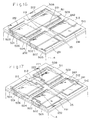
- the coil assembly according to the embodiment illustrated in Fig. 6 is composed of coils each of the structure which corresponds to that described above by reference to Fig. 4. More specifically, the coils 21 to 24 include pairs of coil conductors 211; 212, ..., 241; 242, respectively. Considering the coil conductors 211 and 212, by way of example, they are wound helically around the respective axes which substantially coincide with each other in the winding axis direction O21. Further, the winding direction a1 of the coil conductor 211 is opposite to that b1 of the coil conductor 212 as viewed in the winding axis direction O21.
- the coil conductors 211 and 212 are connected to each other through a connecting portion 213 such that magnetic fields of a same direction are generated by them.
- reference numerals 214 and 215 denote terminals which are connected to given ones of the terminal electrodes 301 to 312 shown in Figs. 1 and 2. It should however be appreciated that the terminal members 214 and 215 may be connected together, wherein the portion connected through the connecting portion 312 may be disconnected or separated to thereby form these terminal members.
- the connecting portion 213 may be used as the leading end with the other coil conductor being stacked thereon.
- the other coils 22 to 24 are implemented basically similarly to the coil 21 and constituted by combinations of the coil conductors 211; 222, ..., 241; 242, respectively, with the winding directions a2; b2, a3; b3 and a4; b4 being opposite to each other, respectively, wherein the respective winding axes coincide substantially with each another, and wherein the individual coil conductors of the coils 22 to 24 are connected, respectively, such that magnetic fields of a same direction are generated.
- the coils 23 and 24 share in common the terminal 25, they may have respective terminals, as is illustrated in Fig. 7 which shows a version of the embodiment shown in Fig. 6. It should further be mentioned that some of the coils 21 to 24 may be implemented equally by a single coil conductor.
- the coil 21 among others. It can be seen that the two coil conductors 211 and 212 constituting the coil 21 are so interconnected that the magnetic fields of a same direction are generated by them. Accordingly, the number N of turns of the coil is equal to a sum (n1 + n2) of the numbers of turns n1 and n2 of the two coil conductors 211 and 212, respectively.
- the inductance value L(H) of the coil is in proportion to a square of a sum of the mumbers of turns n , as described hereinbefore. Thus, there can be realized an extremely high inductance value L.
- both the coils are constituted by helical windings which are offset with a given pitch in the same direction.
- the coil conductors 211 and 212 are opposite to each other in respect to the winding directions a1 and b1, as viewed along the general winding axis O21, wherein the trailing end portion of the coil conductor 211 and the leading end portion of the coil conductor 212 are disposed at the same level in a coplanar relation to each other so as to be easily interconnected by a connecting portion 213.
- the coil conductors 211 and 212 can be connected to each other interiorly of the magnetic material 20, which in turn means that the interconnection can be realized through much simplified and facilitated procedure.
- the other coils 22 to 24 can be constructed in the same manner as described above.
- the coil assembly shown in Fig. 6 may easily be constituted by the individual coils each composed of a greater number of the coil conductors such as described previously in conjunction with Fig. 5.
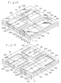
- a method or process for manufacturing the coil layer of the stacked multi-layer composite electric part according to the invention will be made in conjunction with a manufacturing method based on a known lamination process such as disclosed in Japanese Patent Publication No. 39521/1982, it should be understood that there may equally be adopted other film forming techniques such as high-precision patterning technique known as photolithography, sputtering, evaporation, plating or the like. When these methods are adopted, a coil assembly incorporating coil conductors in a higher definition pattern can be implemented in a structure including a greater number of layers.
- magnetic layers 501 and 502 are applied by printing over a surface of a substrate 4 with a space therebetween. More specifically, the magnetic layers 501 and 502 can be formed in a predetermined pattern by applying through a screen printing process a magnetic paste prepared by mixing together pulverized ferrite, a binder and a solvent.
- electric conductors 212, 222, 231 and 241 which are to constitute coil conductors are formed on the magnetic layers 501 and 502, as shown in Fig. 9.
- a screen printing of an electrically conductive paste may be resorted to.
- magnetic layers 503 to 505 are formed in such a manner as to cover the spaces between the magnetic layers 501 and 502 with end portions of the conductors 212, 222, 231 and 241 being exposed, as can be seen in Fig. 10.
- magnetic layers 506 and 507 are so printed as to fill the gaps making appearance among the magnetic layers 503 to 505, as is illustrated in Fig. 12.
- electrical conductors 211 and 221 are formed, respectively, on the magnetic layers 503 and 506 in continuation to the conductors 211 and 221 formed already, while electrical conductors 212 and 222 are formed, respectively, on the magnetic layer 504 and 506 in continuation to the existing conductors 212 and 222.
- electric conductors 231 and 241 are formed on the magnetic layers 504 and 507 in continuation to the conductors 231 and 241, respectively, which have already been formed on the magnetic layer 504.
- electric conductors 232 and 242 are formed on the magnetic layers 505 and 507 in continuation to the conductor 505.
- conductors 211 and 212, the conductors 221 and 222, the conductors 211 and 232 and the conductors 241 and 242 are, respectively, so formed that these paired conductors extend in the directions opposite to each other.
- the coil conductors (211; 212), (221; 222), (231; 232) and (241; 242) each having a desired number of turns are connected together at the leading and trailing ends through connecting portions 213, 223, 233 and 243, respectively, as shown in Fig. 22. In this way, the inductor structure shown in Fig. 6 can be realized.
Landscapes
- Engineering & Computer Science (AREA)
- Power Engineering (AREA)
- Microelectronics & Electronic Packaging (AREA)
- Coils Or Transformers For Communication (AREA)
- Fixed Capacitors And Capacitor Manufacturing Machines (AREA)
Claims (2)
- Elément électrique composite ayant une structure multicouche empilée composée d'une couche à capacités (1) et d'une couche à bobines (2), la couche à bobine (2) comprenant:
au moins une bobine (21, 22, 23, 24) noyée dans une matière magnétique (20),
dans lequel ladite au moins une bobine comprend au moins une combinaison d'au moins deux conducteurs de bobines (200, 201, 202; 211, 212; 221, 222; 231, 232; 241, 242) enroulés en spirale autour d'axes d'enroulements respectifs s'étendant coaxialement l'un avec l'autre, chaque conducteur de bobine étant enroulé dans un sens opposé à celui du conducteur à bobine précédent auquel il est connecté, ce qui entraîne que lesdits conducteurs de bobines sont mutuellement superposés de façon verticale et mutuellement connectés de façon telle que les champs magnétiques générés par lesdits conducteurs de bobines sont dans la même direction. - Elément électrique composite ayant une structure multicouche empilée selon la revendication 1, dans lequel l'extrémité avant de l'un desdits conducteurs de bobines est positionnée au même niveau que l'extrémité arrière du conducteur de bobine précédent, en relation coplanaire l'une avec l'autre.
Applications Claiming Priority (2)
| Application Number | Priority Date | Filing Date | Title |
|---|---|---|---|
| JP38767/90 | 1990-02-20 | ||
| JP2038767A JP3048592B2 (ja) | 1990-02-20 | 1990-02-20 | 積層複合部品 |
Publications (2)
| Publication Number | Publication Date |
|---|---|
| EP0443512A1 EP0443512A1 (fr) | 1991-08-28 |
| EP0443512B1 true EP0443512B1 (fr) | 1995-03-01 |
Family
ID=12534444
Family Applications (1)
| Application Number | Title | Priority Date | Filing Date |
|---|---|---|---|
| EP91102336A Expired - Lifetime EP0443512B1 (fr) | 1990-02-20 | 1991-02-19 | Elément électrique composé ayant une structure multicouche empilée |
Country Status (6)
| Country | Link |
|---|---|
| US (1) | US5157576A (fr) |
| EP (1) | EP0443512B1 (fr) |
| JP (1) | JP3048592B2 (fr) |
| KR (1) | KR950011634B1 (fr) |
| DE (1) | DE69107633T2 (fr) |
| MY (1) | MY105380A (fr) |
Families Citing this family (25)
| Publication number | Priority date | Publication date | Assignee | Title |
|---|---|---|---|---|
| JP2563198Y2 (ja) * | 1992-03-20 | 1998-02-18 | ティーディーケイ株式会社 | 積層型ヘリカルフィルタ |
| JP3141562B2 (ja) * | 1992-05-27 | 2001-03-05 | 富士電機株式会社 | 薄膜トランス装置 |
| EP0588503B1 (fr) * | 1992-09-10 | 1998-10-07 | National Semiconductor Corporation | Circuit intégré d'élément de mémoire magnétique et sa méthode de fabrication |
| DE69323383T2 (de) * | 1992-10-12 | 1999-06-10 | Matsushita Electric Industrial Co., Ltd., Kadoma, Osaka | Verfahren zur Herstellung eines elektronischen Bauelementes |
| JPH06244359A (ja) * | 1993-02-19 | 1994-09-02 | Takashi Murai | 多層チップ |
| US5610433A (en) * | 1995-03-13 | 1997-03-11 | National Semiconductor Corporation | Multi-turn, multi-level IC inductor with crossovers |
| US5831331A (en) * | 1996-11-22 | 1998-11-03 | Philips Electronics North America Corporation | Self-shielding inductor for multi-layer semiconductor integrated circuits |
| JPH10200360A (ja) * | 1997-01-07 | 1998-07-31 | Tdk Corp | 積層バルントランス |
| US6080468A (en) * | 1997-02-28 | 2000-06-27 | Taiyo Yuden Co., Ltd. | Laminated composite electronic device and a manufacturing method thereof |
| JP3055488B2 (ja) * | 1997-03-03 | 2000-06-26 | 日本電気株式会社 | 多層プリント基板及びその製造方法 |
| JPH10261546A (ja) * | 1997-03-19 | 1998-09-29 | Murata Mfg Co Ltd | 積層コンデンサ |
| US5920241A (en) * | 1997-05-12 | 1999-07-06 | Emc Technology Llc | Passive temperature compensating LC filter |
| JP3328168B2 (ja) * | 1997-06-26 | 2002-09-24 | イノテック株式会社 | 半導体デバイス |
| US6380608B1 (en) * | 1999-06-01 | 2002-04-30 | Alcatel Usa Sourcing L.P. | Multiple level spiral inductors used to form a filter in a printed circuit board |
| JP2001036372A (ja) * | 1999-07-15 | 2001-02-09 | Murata Mfg Co Ltd | ディレイライン |
| JP3259717B2 (ja) * | 1999-08-20 | 2002-02-25 | 株式会社村田製作所 | 積層型インダクタ |
| FR2823365B1 (fr) * | 2001-04-05 | 2003-08-15 | Sbea Technologies | Enroulement electrique, son procede de realisation et composant electromagnetique integrant au moins un tel enroulement |
| US6667536B2 (en) | 2001-06-28 | 2003-12-23 | Agere Systems Inc. | Thin film multi-layer high Q transformer formed in a semiconductor substrate |
| US6639298B2 (en) | 2001-06-28 | 2003-10-28 | Agere Systems Inc. | Multi-layer inductor formed in a semiconductor substrate |
| JP2006278566A (ja) * | 2005-03-28 | 2006-10-12 | Tdk Corp | 積層電子部品及びその製造方法 |
| US8558636B2 (en) * | 2007-03-30 | 2013-10-15 | Intel Corporation | Package embedded equalizer |
| JP5447503B2 (ja) * | 2009-03-18 | 2014-03-19 | 株式会社村田製作所 | 電子部品 |
| JP6050667B2 (ja) * | 2012-12-04 | 2016-12-21 | デクセリアルズ株式会社 | コイルモジュール、非接触電力伝送用アンテナユニット、及び電子機器 |
| JP6329422B2 (ja) * | 2014-04-21 | 2018-05-23 | オリンパス株式会社 | 医療器具、挿入補助具、および医療システム |
| KR102194727B1 (ko) | 2015-04-29 | 2020-12-23 | 삼성전기주식회사 | 인덕터 |
Family Cites Families (7)
| Publication number | Priority date | Publication date | Assignee | Title |
|---|---|---|---|---|
| GB1440304A (en) * | 1974-11-29 | 1976-06-23 | Mullard Ltd | Transmission line pulse transformers |
| FR2379229A1 (fr) * | 1977-01-26 | 1978-08-25 | Eurofarad | Composants electroniques multi-couches inductifs et leur procede de fabrication |
| GB2045540B (en) * | 1978-12-28 | 1983-08-03 | Tdk Electronics Co Ltd | Electrical inductive device |
| US4613843A (en) * | 1984-10-22 | 1986-09-23 | Ford Motor Company | Planar coil magnetic transducer |
| JPS6427305A (en) * | 1987-07-22 | 1989-01-30 | Murata Manufacturing Co | Lc filter |
| US4959631A (en) * | 1987-09-29 | 1990-09-25 | Kabushiki Kaisha Toshiba | Planar inductor |
| EP0411922B1 (fr) * | 1989-08-01 | 1994-03-30 | TDK Corporation | Inductances du type à enroulements composés, à couches empilées comprenant des inductances ayant une auto-inductance et ayant une inductance mutuelle et leur méthode de fabrication |
-
1990
- 1990-02-20 JP JP2038767A patent/JP3048592B2/ja not_active Expired - Fee Related
-
1991
- 1991-02-19 DE DE69107633T patent/DE69107633T2/de not_active Expired - Fee Related
- 1991-02-19 US US07/657,699 patent/US5157576A/en not_active Expired - Lifetime
- 1991-02-19 MY MYPI91000264A patent/MY105380A/en unknown
- 1991-02-19 EP EP91102336A patent/EP0443512B1/fr not_active Expired - Lifetime
- 1991-02-20 KR KR1019910002738A patent/KR950011634B1/ko not_active Expired - Fee Related
Also Published As
| Publication number | Publication date |
|---|---|
| DE69107633T2 (de) | 1995-10-19 |
| JP3048592B2 (ja) | 2000-06-05 |
| JPH03241862A (ja) | 1991-10-29 |
| DE69107633D1 (de) | 1995-04-06 |
| KR920000206A (ko) | 1992-01-10 |
| EP0443512A1 (fr) | 1991-08-28 |
| US5157576A (en) | 1992-10-20 |
| KR950011634B1 (ko) | 1995-10-07 |
| MY105380A (en) | 1994-09-30 |
Similar Documents
| Publication | Publication Date | Title |
|---|---|---|
| EP0443512B1 (fr) | Elément électrique composé ayant une structure multicouche empilée | |
| US6222427B1 (en) | Inductor built-in electronic parts using via holes | |
| EP0433176B1 (fr) | Circuit hybride multi-couche | |
| US5602517A (en) | Laminate type LC composite device having coils with opposing directions and adjacent leads | |
| EP0933788B1 (fr) | Composant électronique multicouche et sa méthode de fabrication | |
| US6249205B1 (en) | Surface mount inductor with flux gap and related fabrication methods | |
| JPH06333742A (ja) | 積層コイル | |
| JP3186776B2 (ja) | 電子部品の製造方法 | |
| JPH01151211A (ja) | 積層応用部品の構造 | |
| JP2682829B2 (ja) | 積層応用部品の構造 | |
| JP2986520B2 (ja) | 電子部品及びその製造方法 | |
| JPH0993069A (ja) | 多連ノイズフィルタ | |
| JPH06302436A (ja) | 積層型ノイズ吸収素子複合体 | |
| JPH038311A (ja) | 積層型トランス | |
| JP3048593B2 (ja) | 混成集積回路部品 | |
| JPH04101403A (ja) | 電子部品及びその製造方法 | |
| JP2835122B2 (ja) | 積層複合部品とその製造方法 | |
| JPS5928305A (ja) | インダクタンス素子とその製造方法 | |
| JPH0878991A (ja) | チップ型lcフィルタ素子 | |
| JPH04101404A (ja) | 電子部品及びその製造方法 | |
| JPH0238410Y2 (fr) | ||
| JPH0729815U (ja) | 積層lcフィルタおよびこれを用いた複合積層lcフィルタ | |
| JPH04276609A (ja) | 電子部品 | |
| JPH03159206A (ja) | 混成集積回路部品の構造 | |
| JPH04106910A (ja) | 電子部品 |
Legal Events
| Date | Code | Title | Description |
|---|---|---|---|
| PUAI | Public reference made under article 153(3) epc to a published international application that has entered the european phase |
Free format text: ORIGINAL CODE: 0009012 |
|
| AK | Designated contracting states |
Kind code of ref document: A1 Designated state(s): DE FR GB |
|
| 17P | Request for examination filed |
Effective date: 19920227 |
|
| 17Q | First examination report despatched |
Effective date: 19920520 |
|
| GRAA | (expected) grant |
Free format text: ORIGINAL CODE: 0009210 |
|
| AK | Designated contracting states |
Kind code of ref document: B1 Designated state(s): DE FR GB |
|
| REF | Corresponds to: |
Ref document number: 69107633 Country of ref document: DE Date of ref document: 19950406 |
|
| ET | Fr: translation filed | ||
| PLBE | No opposition filed within time limit |
Free format text: ORIGINAL CODE: 0009261 |
|
| STAA | Information on the status of an ep patent application or granted ep patent |
Free format text: STATUS: NO OPPOSITION FILED WITHIN TIME LIMIT |
|
| 26N | No opposition filed | ||
| REG | Reference to a national code |
Ref country code: GB Ref legal event code: IF02 |
|
| REG | Reference to a national code |
Ref country code: GB Ref legal event code: 746 Effective date: 20021121 |
|
| REG | Reference to a national code |
Ref country code: FR Ref legal event code: D6 |
|
| PGFP | Annual fee paid to national office [announced via postgrant information from national office to epo] |
Ref country code: FR Payment date: 20050208 Year of fee payment: 15 |
|
| PGFP | Annual fee paid to national office [announced via postgrant information from national office to epo] |
Ref country code: GB Payment date: 20050216 Year of fee payment: 15 |
|
| PGFP | Annual fee paid to national office [announced via postgrant information from national office to epo] |
Ref country code: DE Payment date: 20050217 Year of fee payment: 15 |
|
| PG25 | Lapsed in a contracting state [announced via postgrant information from national office to epo] |
Ref country code: GB Free format text: LAPSE BECAUSE OF NON-PAYMENT OF DUE FEES Effective date: 20060219 |
|
| PG25 | Lapsed in a contracting state [announced via postgrant information from national office to epo] |
Ref country code: DE Free format text: LAPSE BECAUSE OF NON-PAYMENT OF DUE FEES Effective date: 20060901 |
|
| GBPC | Gb: european patent ceased through non-payment of renewal fee |
Effective date: 20060219 |
|
| REG | Reference to a national code |
Ref country code: FR Ref legal event code: ST Effective date: 20061031 |
|
| PG25 | Lapsed in a contracting state [announced via postgrant information from national office to epo] |
Ref country code: FR Free format text: LAPSE BECAUSE OF NON-PAYMENT OF DUE FEES Effective date: 20060228 |