EP0444712A1 - Mehrfachgatter-Dünnfilmtransistor - Google Patents
Mehrfachgatter-Dünnfilmtransistor Download PDFInfo
- Publication number
- EP0444712A1 EP0444712A1 EP91103223A EP91103223A EP0444712A1 EP 0444712 A1 EP0444712 A1 EP 0444712A1 EP 91103223 A EP91103223 A EP 91103223A EP 91103223 A EP91103223 A EP 91103223A EP 0444712 A1 EP0444712 A1 EP 0444712A1
- Authority
- EP
- European Patent Office
- Prior art keywords
- gate
- thin film
- film transistor
- gates
- transistor
- Prior art date
- Legal status (The legal status is an assumption and is not a legal conclusion. Google has not performed a legal analysis and makes no representation as to the accuracy of the status listed.)
- Granted
Links
Images










Classifications
-
- H—ELECTRICITY
- H10—SEMICONDUCTOR DEVICES; ELECTRIC SOLID-STATE DEVICES NOT OTHERWISE PROVIDED FOR
- H10D—INORGANIC ELECTRIC SEMICONDUCTOR DEVICES
- H10D30/00—Field-effect transistors [FET]
- H10D30/60—Insulated-gate field-effect transistors [IGFET]
- H10D30/67—Thin-film transistors [TFT]
- H10D30/6729—Thin-film transistors [TFT] characterised by the electrodes
- H10D30/673—Thin-film transistors [TFT] characterised by the electrodes characterised by the shapes, relative sizes or dispositions of the gate electrodes
- H10D30/6733—Multi-gate TFTs
- H10D30/6734—Multi-gate TFTs having gate electrodes arranged on both top and bottom sides of the channel, e.g. dual-gate TFTs
-
- H—ELECTRICITY
- H10—SEMICONDUCTOR DEVICES; ELECTRIC SOLID-STATE DEVICES NOT OTHERWISE PROVIDED FOR
- H10D—INORGANIC ELECTRIC SEMICONDUCTOR DEVICES
- H10D30/00—Field-effect transistors [FET]
- H10D30/60—Insulated-gate field-effect transistors [IGFET]
- H10D30/67—Thin-film transistors [TFT]
- H10D30/6729—Thin-film transistors [TFT] characterised by the electrodes
- H10D30/673—Thin-film transistors [TFT] characterised by the electrodes characterised by the shapes, relative sizes or dispositions of the gate electrodes
- H10D30/6733—Multi-gate TFTs
-
- H—ELECTRICITY
- H10—SEMICONDUCTOR DEVICES; ELECTRIC SOLID-STATE DEVICES NOT OTHERWISE PROVIDED FOR
- H10D—INORGANIC ELECTRIC SEMICONDUCTOR DEVICES
- H10D30/00—Field-effect transistors [FET]
- H10D30/60—Insulated-gate field-effect transistors [IGFET]
- H10D30/611—Insulated-gate field-effect transistors [IGFET] having multiple independently-addressable gate electrodes influencing the same channel
-
- H—ELECTRICITY
- H10—SEMICONDUCTOR DEVICES; ELECTRIC SOLID-STATE DEVICES NOT OTHERWISE PROVIDED FOR
- H10D—INORGANIC ELECTRIC SEMICONDUCTOR DEVICES
- H10D30/00—Field-effect transistors [FET]
- H10D30/60—Insulated-gate field-effect transistors [IGFET]
- H10D30/67—Thin-film transistors [TFT]
- H10D30/6704—Thin-film transistors [TFT] having supplementary regions or layers in the thin films or in the insulated bulk substrates for controlling properties of the device
-
- H—ELECTRICITY
- H10—SEMICONDUCTOR DEVICES; ELECTRIC SOLID-STATE DEVICES NOT OTHERWISE PROVIDED FOR
- H10D—INORGANIC ELECTRIC SEMICONDUCTOR DEVICES
- H10D30/00—Field-effect transistors [FET]
- H10D30/60—Insulated-gate field-effect transistors [IGFET]
- H10D30/67—Thin-film transistors [TFT]
- H10D30/6704—Thin-film transistors [TFT] having supplementary regions or layers in the thin films or in the insulated bulk substrates for controlling properties of the device
- H10D30/6713—Thin-film transistors [TFT] having supplementary regions or layers in the thin films or in the insulated bulk substrates for controlling properties of the device characterised by the properties of the source or drain regions, e.g. compositions or sectional shapes
-
- H—ELECTRICITY
- H10—SEMICONDUCTOR DEVICES; ELECTRIC SOLID-STATE DEVICES NOT OTHERWISE PROVIDED FOR
- H10D—INORGANIC ELECTRIC SEMICONDUCTOR DEVICES
- H10D30/00—Field-effect transistors [FET]
- H10D30/60—Insulated-gate field-effect transistors [IGFET]
- H10D30/67—Thin-film transistors [TFT]
- H10D30/6729—Thin-film transistors [TFT] characterised by the electrodes
- H10D30/6737—Thin-film transistors [TFT] characterised by the electrodes characterised by the electrode materials
- H10D30/6739—Conductor-insulator-semiconductor electrodes
-
- H—ELECTRICITY
- H10—SEMICONDUCTOR DEVICES; ELECTRIC SOLID-STATE DEVICES NOT OTHERWISE PROVIDED FOR
- H10D—INORGANIC ELECTRIC SEMICONDUCTOR DEVICES
- H10D30/00—Field-effect transistors [FET]
- H10D30/60—Insulated-gate field-effect transistors [IGFET]
- H10D30/67—Thin-film transistors [TFT]
- H10D30/674—Thin-film transistors [TFT] characterised by the active materials
- H10D30/6741—Group IV materials, e.g. germanium or silicon carbide
- H10D30/6743—Silicon
- H10D30/6745—Polycrystalline or microcrystalline silicon
-
- H—ELECTRICITY
- H10—SEMICONDUCTOR DEVICES; ELECTRIC SOLID-STATE DEVICES NOT OTHERWISE PROVIDED FOR
- H10D—INORGANIC ELECTRIC SEMICONDUCTOR DEVICES
- H10D30/00—Field-effect transistors [FET]
- H10D30/60—Insulated-gate field-effect transistors [IGFET]
- H10D30/67—Thin-film transistors [TFT]
- H10D30/6757—Thin-film transistors [TFT] characterised by the structure of the channel, e.g. transverse or longitudinal shape or doping profile
-
- H—ELECTRICITY
- H10—SEMICONDUCTOR DEVICES; ELECTRIC SOLID-STATE DEVICES NOT OTHERWISE PROVIDED FOR
- H10D—INORGANIC ELECTRIC SEMICONDUCTOR DEVICES
- H10D8/00—Diodes
Definitions
- the present invention relates to a thin film transistor suitable for use as a switching element, and more specifically to a thin film transistor of a small off current or of a high on/off current ratio.
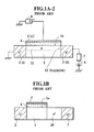
- FIG. 1A A prior-art thin film transistor is well known as shown in Fig. 1A, in which only the basic transistor structure is diagrammatically depicted.
- the transistor includes a channel forming region 1, source and drain regions 2 and 3, a gate insulating film 4, and a gate electrode 5.
- the channel forming region 1 is a semiconductor thin film formed of polysilicon or amorphous silicon, for instance having neither n-type nor p-type impurity doped intentionally or having a sufficiently low n-type or p-type impurity concentration.
- the source and drain regions 2 and 3 are a semiconductor thin film formed of polysilicon or amorphous silicon, for instance having a sufficiently high n-type or p-type impurity concentration, respectively as compared with that of the channel forming region, and arranged at first and second different positions adjoining to the channel forming region 1, respectively.
- the gate electrode 5 is formed over a principal plane 1a of the channel forming region 1 and between the source region 2 and the drain region 3, via the gate insulating film 4 formed of silicon oxide, for instance.
- the prior-art thin film transistor shown in Fig. 1A can be preferably used as a switching element.
- this prior-art thin film transistor shown in Fig. 1B is basically the same in structure as the previous prior-art transistor shown in Fig. 1A except that an offset region 20 of a semiconductor thin film formed of polysilicon or amorphous silicon, for instance having an n-type impurity concentration lower than that of the drain region 3 is interposed between the channel forming region 1 and the drain region 3. Therefore, the same reference numerals have been retained for similar elements which have the same functions, without repeating any detailed description of them.
- a negative control voltage is applied by the control voltage supply 8 to the gate electrode 5 with the source region 2 as zero voltage level, as shown in Fig. 1B-2
- a p-type channel layer 11 is formed within the channel forming region 1 and under the gate electrode 5 so as to expand from the gate insulating film 4 in the direction opposite to the gate electrode 5 and extend between the source region 2 and the offset region 20 in the same way as with the case of the prior-art transistor shown in Fig. 1A, a backward pn function 13 is formed between the n-type offset region 20 and the p-type channel layer 11, so that the range between the source and drain regions 2 and 3 is turned off and therefore current is not supplied from the voltage supply to the load 7.
- the prior-art thin film transistor shown in Fig. 1B can be preferably used as a switching element in the same way as with the case of the prior-art transistor shown in Fig. 1A.
- the p-type channel layer 11 is formed within the channel forming region 1 when the transistor is turned from on (as shown in Fig. 1A-1) to off (as shown in Fig. 1A-2).
- a depletion layer is formed at the pn junction 12 between the n-type drain region 3 and the p-type channel layer 11 in such a way as to extend toward both the drain region 3 and the channel layer 11, respectively.
- the drain region 3 is formed of a semiconductor having a relatively high n-type impurity atom concentration, the width of the depletion layer extending toward the drain region is relatively narrow.
- the depletion layer existing at this pn junction 12 is relatively narrow in width, when the transistor is kept turned off, a relatively high electric field is generated at the depletion layer of the pn junction 12 between the drain region 3 and the channel layer 11, so that there exists a problem in that a relatively large leakage current flows from the drain region 3 to the source region 2 through traps existing at the depletion layer extending between the drain region 3 and the channel layer 11 in the transistor turn-off state.
- a p-type channel layer 11 is formed within the channel forming region 1 when the transistor is turned from on (as shown in Fig. 1B-1) to off (as shown in Fig. 1B-2).
- a depletion layer is formed at the pn junction 13 between the n-type offset region 20 and the p-type channel layer 11 in such a way as to extend toward both the offset region 20 and the channel layer 11, respectively.
- the width of the depletion layer extending toward the offset region 20 is relatively wide. That is, since the depletion layer existing at the pn junction 13 is relatively wide in width, when the transistor is kept turned off, a relatively low electric field is generated at the depletion layer at the pn junction 13 between the offset region 20 and the channel layer 11, so that a relatively low leakage current flows from the drain region 3 to the source region 2 through defects existing (if any) at both the depletion layers extending toward the offset range 3 and the channel layer 11 in the transistor turn-off state. That is, in the transistor shown in Fig. 1B, it is possible to markedly reduce the leakage current flowing from the drain region 3 to the source region 2 when the transistor is kept turned off.
- the primary object of the present invention is to provide a novel thin film transistor which can increase the on current and decrease the off current flowing between the drain region and the source region, that is, can improve the on/off current ratio of the thin film transistor.
- the thin film transistor according to the present invention comprises: (a) a source region (2) formed of a first conductive type semiconductor film; (b) a drain region (3) formed of the first conductive type semiconductor film; (c) a channel forming region (1) formed of a semiconductor thin film having a low impurity concentration between said source and drain regions; (d) a first gate (51) formed over a first principal plane (1a) of said channel forming region via a first gate insulating film (41), for turning on or off the thin film transistor; and (e) a second gate (52) formed over said channel forming region via a second gate insulating film (42), for reducing current flowing between said source and drain regions when the transistor is turned off.
- first and second voltages are applied to said first and second gates (51, 52) to form first conductive type channel layers (101, 102) in said channel forming region under said first and second gate insulating films (41, 42) when the transistor is turned on, but a third voltage opposite to the first voltage is applied to the first gate (51) to form a second conductive type channel layer (103) in said channel forming region under said first gate insulating film (41) and the second voltage is applied to the second gate (52) to form the first conductive type channel layer (102) in said channel forming region under said second gate insulating film (42) when the transistor turned off, so that a pn junction (100) is formed in said channel forming region (1) under between said first and second gate insulating films (41, 42) to reduce off current flowing between said source and drain regions.
- first and second voltages are applied to said first and second gates (51, 52) to form a first conductive type channel layers (101, 102) in said channel forming region under said first and second gate insulating films (41, 42) when the transistor is turned on, but a third voltage opposite to the first voltage is applied to the first and second gates to form a second conductive type channel layer (103) in said channel forming region under said second gate insulating film (42) and the same second conductive type channel layer (104) having a carrier concentration lower than that (103) under said first gate insulating film (41) in said channel forming region under said second gate insulating film (42) when the transistor is turned off, so that a wide depletion layer (110) is formed between said source or drain region (2, 3) and the second conductive type semiconductor layer (104) to reduce off current flowing between said source and drain regions.
- said first gate (51) and said second gate (52) are formed on a first principal plane (1a) of said channel forming region.
- said first gate (51) is formed on a first principal plane (1a) of said channel forming region and said second gate (52) is formed on a second principal plane (1b) opposite to the first principal plane of said channel forming region.
- the transistor further comprises a third gate (53) formed over said channel forming region via a third gate insulating film (53) so as to sandwich the first gate between said second and third gates, and further said first gate (51) and said second and third gates (52, 53) are all formed on a first principal plane (1a) of said channel forming region.
- the transistor further comprises a third gate (53) formed over said channel forming region via a third gate insulating film (43) so as to sandwich the first gate between said second and third gates, and further said first gate (51) is formed on a first principal plane (1a) of said channel forming region and said second and third gates (52, 53) are formed on a second principal plane (1b) opposite to the first principal plane of said channel forming region.
- a diode or a capacitor is connected from the first gate to the second gate, or a conductive wire or a diode is connected from the drain region to the second gate.
- two diodes or two capacitors are connected from the first gate to the second and third gates, or conductive wires or diodes are connected from the drain region to the second and third gates, respectively.
- the thin film transistor according to the present invention since at least one subgate is provided in addition to the main gate, it is possible to form at least one pn junction induced by two different polarity electric fields in the channel forming region under between the source and drain region by applying a first voltage to the main gate and a second voltage to the subgate when the transistor turned off. As a result, it is possible to markedly reduce the turn-off leakage current flowing between the source and drain regions.
- the thin film transistor can be used in the same way as the ordinary three-terminal transistors.
- the thin film transistor can be formed in accordance with the ordinary transistor manufacturing process, without any special manufacturing steps, it is possible to improve the production yield and therefore manufacture the thin film transistor at low cost.
- the feature of the present invention is to provide at least one additional subgate to the ordinary thin film transistor having a source, a drain and a gate, to reduce the turn-off leakage current.
- the present invention will be explained in detail hereinbelow by taking the case of n-channel thin film transistor by way of example. However, it is of course possible to apply the present invention to p-channel thin film transistor.
- Fig. 2 shows a first embodiment thereof.
- the thin film transistor comprises a channel forming region 1, a source region 2, a drain region 3, a first gate insulating film 41, a second gate insulating film 42, a first gate electrode 51, and a second gate electrode 52.
- the channel forming region 1 is formed of a semiconductor thin film having neither n-type nor p-type impurity doped intentionally or a sufficiently low n-type or p-type impurity concentration.
- the source and drain regions 2 and 3 are formed of a semiconductor thin film having a sufficiently high n-type or p-type impurity concentration, respectively, as compared with that of the channel forming region 1, at first and second positions adjoining to the channel forming region 1, respectively.
- the source and drain regions 2 and 3 can be formed by implanting n-type or p-type impurity into the channel forming region 1 of a polycrystal semiconductor (e.g. polysilicon) at two different positions (two opposing sides) of the channel forming region 1.
- a polycrystal semiconductor e.g. polysilicon
- the channel forming region 1 is a range formed between the source and drain regions 2 and 3 by implanting impurity into a thin film substrate. Further, it is also possible to form the semiconductor thin film of the source and drain regions 2 and 3 separately from the semiconductor thin film of the channel forming region 1.
- the semiconductor thin film of the channel forming region 1 and the source and drain regions 2 and 3 is a microcrystal, polycrystal or amorphous semiconductor.
- the first gate electrode 51 is formed over a principal plane 1a of the channel forming region 1 and near the source region 2 so as to cover a range between the source and drain regions 2 and 3, via a first gate insulating film 41.
- the second gate electrode 52 is also formed over the principal plane 1a of the channel forming region 1 and near the drain region 3 so as to cover a range between the source and drain regions 2 and 3 over which the first gate electrode 51 is not formed, via a second gate insulating film 42.
- the first and second gate insulating films 41 and 42 are physically connected to each other or overlapped and extend all over the principal plane 1a between the source and drain regions 2 and 3. Further, although not shown, the first and second gate electrodes 51 and 52 are physically overlapped or connected to or disconnected from each other.
- the first and second gate insulating films 41 and 42 are formed of the same material (e.g. SiO2), and the thickness of the first gate insulating film 41 is the same as that of the second gate insulating film 42.
- a first n-type channel layer 101 is formed within the channel forming region 1 and under the first gate electrode 51 so as to expand from the first gate insulating film 41 in the direction opposite to the first gate electrode 51 and extend to the source region 2
- a second n-type channel layer 102 is formed within the channel forming region 1 and under the second gate electrode 52 so as to expand from the second gate insulating film 42 in the direction opposite to the second gate electrode 52 and extend to the drain region 3
- the range between the source and drain regions 2 and 3 are turned on, so that current is supplied from the voltage supply 6 to the load 7.
- a negative control voltage is applied from the first control voltage supply 81 to only the first gate electrode 51 with the source region 2 as zero voltage level as shown in Fig. 2-2
- a third p-type channel layer 103 is formed within the channel forming region 1 and under the first gate electrode 51 so as to expand from the first gate insulating film 41 in the direction opposite to the first gate electrode 51 and extend to the source region 2
- a backward drain pn junction 100 is formed between the second and third channel layers 102 and 103 in reverse polarity relationship with respect to the voltage supply 6, so that the range between the source and drain regions 2 and 3 is turned off and therefore current is not supplied from the voltage supply 6 to the load 7.
- the thin film transistor shown in Fig. 2 can be preferably used as a switching element.
- the drain junction 12 is formed between the drain region 3 and the p-type channel layer 11 formed under the first (main) gate 5.
- an effective drain junction 100 is formed between the n-type channel layer 102 induced by an electric field under the second (sub) gate 52 and the p-type channel layer 103 formed under the first (main) gate 51, as depicted in Fig. 2-2.
- the drain junction 12 formed between the drain region 3 and the channel layer 11 there exists a problem in that many additional traps are inevitably produced during the manufacturing process (e.g. during the source and drain formation process) and therefore leakage current inevitably flows therethrough.
- the traps are lattice defects or impurity atoms which acquire carriers (i.e. electrons and holes).
- the carrier concentration must be decreased and therefore the resistance must be increased in the offset area 20 in order to reduce the off current.
- the n-type layer carrier concentration formed under the second gate electrode can be controlled by changing the voltage applied to the second electrode, the film thickness, the dielectric constant and the fixed charge of the second gate insulating film, without exerting any influence upon the off current characteristics, there exists an advantage in that it is possible to easily prevent the on current from being reduced.
- Fig. 2A shows a first modification of the first embodiment of the thin film transistor according to the present invention, in which the thickness of the second gate insulating film 42 is determined smaller than that of the first gate insulating film 41.
- this modification as far as the absolute value of the gate voltage applied to the first and second gate electrodes 51 and 52 is constant, since a higher electric field is generated under the second gate electrode 52 via the second thin gate insulating film 42, it is possible to increase the carrier concentration (n+) in the channel layer 104 formed under the second gate electrode 52, so that it is possible to eliminate a difference in carrier concentration between the drain 3 and the channel layer 104. Therefore, there exists such an advantage that the on current can be increased as compared with the transistor shown in Fig. 2.
- Fig. 2B shows a second modification of the first embodiment, in which the dielectric constant ⁇ 2 of the second gate insulating film 42 is determined larger than that ⁇ 1 of the first gate insulating film 41.
- this modification as far as the absolute value of the gate voltage is constant, since a higher electric field is generated under the second gate electrode 52, it is possible to increase the carrier concentration (n+) in the channel layer 104 formed under the second gate electrode 52, thus increasing the on current in the same way as in the first modification of the first embodiment shown in Fig. 2A.
- Fig. 2C shows a third modification of the first embodiment, in which the fixed charge Q2 of the second gate insulating film 42 is determined much larger than that Q1 of the first gate insulating film 41.
- this modification since a higher electric field is generated under the second gate electrode 52, it is possible to obtain the same advantage as in the first and second modifications of the first embodiment shown in Figs. 2A and 2B.
- the turn-off leakage current is reduced by the drain junction 100 formed between the third and fourth channel layers 103 and 104 within the channel forming region 1.
- the turn-off leakage current is reduced by the drain junction 110 formed between the drain region 3 and the fourth channel layer 104.
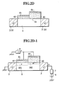
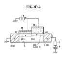
- Fig. 2D shows a fourth modification of the first embodiment, in which the thickness of the second gate insulating film 42 is determined larger than that of the first gate insulating film 41, being different from the first embodiment shown in Fig. 2.
- Fig. 2D-1 when a positive control voltage is applied from a common control voltage supply 8 to the first and second gate electrodes 51 and 52 with the source region 2 as zero voltage level, under the condition that a positive voltage is applied to the drain region 3 from a voltage supply 6 via a load 7, since a first n-type channel layer 101 is formed within the channel forming region 1 and under the first gate electrode 51 so as to expand from the first gate insulating film 41 in the direction opposite to the first gate electrode 51 and extend to the source region 2, and additionally a second n-type channel layer 102 is formed within the channel forming region 1 and under the second gate electrode 52 so as to expand from the second gate insulating film 42 in the direction opposite to the second gate electrode 52 and extend to the drain region 3 and the first channel layer 101, the range between the source and drain regions 2 and 3 are turned on, so that current is supplied from the voltage supply 6 to the load 7.
- a negative control voltage is applied from the control voltage supply 8 to the first and second gate electrodes 51 and 52 with the source region 2 as zero voltage level as shown in Fig. 2D-2
- a third p-type channel layer 103 is formed within the channel forming region 1 and under the first gate electrode 51 so as to expand from the first gate insulating film 41 in the direction opposite to the first gate electrode 51 and extend to the source region 2
- a fourth p-type channel layer 104 is formed within the channel forming region 1 and under the second gate electrode 52 so as to expand from the second gate insulating film 42 in the direction opposite to the second gate electrode 52 and extend to the drain region 3 and the third channel layer 103
- a pn junction 110 is formed between the drain region 3 and the fourth channel layer 104 in reverse polarity relationship with respect to the voltage supply 6, so that the range between the source and drain regions 2 and 3 is turned off and therefore current is not supplied from the voltage supply 6 to the load 7.
- the third and fourth p-type channel layers 103 and 104 are formed within the channel forming region 1 when the transistor is turned from on (as shown in Fig. 2D-1) to off (as shown in Fig. 2D-2).
- a depletion layer is formed at the pn junction 110 between the n-type drain region 3 and the fourth p-type channel layer 104 in such a way as to extend toward both the drain region 3 and the fourth channel layer 104, respectively.
- the fourth channel layer 104 can be formed by a low electric field due to the thick second gate insulating film 42, the carrier concentration of the fourth channel layer 104 is sufficiently low. Therefore, it is possible to widen the width of the depletion layer extending toward the fourth channel layer 104. That is, the depletion layer 110 formed between the drain region 3 and the fourth channel layer 104 is relatively wide.
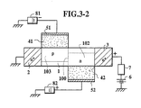
- Fig. 3 shows a second embodiment of the thin film transistor according to the present invention.
- the second gate electrode 52 and the second gate insulating film 42 are formed on another principal plane of the channel forming layer 1.
- first gate electrode 51 and the first gate insulating film 41 are formed on a first principal plane 1a of the channel forming region 1
- second gate electrode 52 and the second gate insulating film 42 are formed on a second principal plane 1b opposite to the first principal plane 1a.
- Fig. 3-1 shows the turn-on state where two positive control voltages are applied to the first and second gate electrodes 51 and 52, respectively and Fig. 3-2 shows the turn-off state where a negative control voltage is applied to the first gate electrode 51 and the positive control voltage is kept applied to the second gate electrode 52.
- an effective drain junction 100 is formed between the n-type channel layer 102 induced by an electric field under the second (sub-) gate electrode 52 and the p-type channel layer 103 formed under the first (main) gate electrode 51, as depicted in Fig. 3-2. Therefore, it is possible to markedly reduce the leakage current when the transistor is kept turned off.
- Fig. 4 shows a third embodiment of the thin film transistor according to the present invention.
- a third control (second sub-) gate insulating film 43 is additionally formed on the same principal plane 1a of the channel forming region 1 in such a way that the first (main) gate electric 51 is interposed between the second and third (two sub-) gate electrodes 52 and 53.
- Fig. 4-1 shows the turn-on state where two positive control voltages are applied to the first, second and third gate electrodes 51, 52 and 53, respectively and Fig. 4-2 shows the turn-off state where a negative control voltage is applied to the first gate electrode 51 and the positive control voltage is kept applied to the second and third gate electrodes 52 and 53.
- two effective drain junctions 100A and 100B can be formed between the p-type channel layer 103 formed under the first (main) gate electrode 51 and the n-type channel layers 102A and 102B induced by two electric fields under the second and third (two sub-) gate electrodes 52 and 53, respectively.
- the structure is such that a positive voltage is always applied to the first gate electrode, and the on/off states of the thin film transistor is controlled by a voltage applied to the second and third gate electrodes.
- a negative voltage is applied to the second and third gate electrodes, p regions are formed under the second and third gate electrodes. Therefore, since two pn junctions 100A and 100B are formed between the p regions and the middle n region always formed under the first gate electrode as shown in Fig.
- the feature of this embodiment is as follows: Since the n region formed under the first gate electrode is not directly connected to the source electrode under the turn-on condition, it is possible to increase the on current even if the carrier concentration of this area is not so high. Accordingly, these exists an advantage such that it is possible to reduce the voltage always applied to the first gate electrode.
- Fig. 5 shows a fourth embodiment of the thin film transistor according to the present invention.
- the second and third gate electrodes 52 and 53 and the second and third gate insulating films 42 and 43 are formed on another principal plane 1b of the channel forming layer 1.
- first gate electrode 51 and the first gate insulating film 41 are formed on a first principal plane 1a of the channel forming region 1
- second and third gate electrodes 52 and 53 and the second and third gate insulating films 42 and 43 are formed on a second principal plane 1b opposite to the first principal plane 1a.
- Fig. 5-1 shows the turn-on state where two positive control voltages are applied to the first, second and third gate electrodes 51, 52 and 53, respectively and Fig. 5-2 shows the turn-off state where a negative control voltage is applied to the first gate electrode 51 and the positive control voltage is kept applied to the second and third gate electrodes 52 and 53.
- effective drain junction 100A is formed between the n-type channel layer 102A induced by an electric field under the second (sub-) gate electrode 52 and the p-type channel layer 103 formed under the first (main) gate electrode 51, as depicted in Fig. 5-2. Therefore, it is possible to securely reduce the leakage current when the transistor is kept turned off.
- the structure is such that a positive voltage is always applied to the first gate electrode, and the on/off states of the thin film transistor is controlled by a voltage applied to the second and third gate electrodes.
- a negative voltage is applied to the second and third gate electrodes, p regions are formed under the second and third gate electrodes. Therefore, since two pn junctions 100A and 100B are formed between the p regions and the middle n region always formed under the first gate electrode as shown in Fig.
- the n region formed under the first gate electrode is not directly connected to the source electrode under the turn-on condition, it is possible to increase the on current even if the carrier concentration of this area is not so high. Accordingly, these exists an advantage such that it is possible to reduce the voltage always applied to the first gate electrode.
- Figs. 6A and 6B show more practical cross-sectional views showing the third embodiment of the thin film transistor using a pn junction produced by the gate voltage shown in Figs. 4, 4-1, and 4-2.
- the thin film transistor is formed on an insulating glass substrate 60 in such a way that the first gate electrode 51 is separated from the second and third gate electrodes 52 and 53.
- Fig. 6C shows a similar more practical cross-sectional view showing the third embodiment of the thin film transistor using a pn junction produced by the gate voltage shown in Figs. 4, 4-1, and 4-2.
- the source and drain regions 2 and 3 are formed by a manufacturing step different from that of forming the channel forming region 1.
- Figs. 7A and 7B show more practical cross-sectional views showing the sixth modification of the third embodiment of the thin film transistor using a wide depletion layer shown in Figs. 4, 4-1, and 4-2.
- the thin film transistor is formed on an insulating glass substrate 60 in such a way that the first gate electrode 51 is connected to the second and third gate electrodes 52 and 53.
- Figs. 8A and 8B show more practical cross-sectional views showing the fourth embodiment of the thin film transistor shown in Figs. 5, 5-1, and 5-2.
- the thin film transistor is formed on an insulating glass substrate 60 in such a way that the first gate electrode 51 is separated from the second and third gate electrodes 52 and 53.
- the transistor since at least one subgate is additionally formed, the transistor is of four-terminal element.
- the transistor since the fourth modification of the first embodiment as shown in Fig. 2D, since the first (main) gate electrode 51 is connected externally to the second or third (sub-) gate electrode 52 or 53, it is possible to consider these modifications as three-terminal elements.
- the manufacturing process of the first embodiment is not so complicated, as compared with that of the prior-art thin film transistor shown in Fig. 2A in which an offset region 20 of a semiconductor thin film is additionally formed between the channel forming region 1 and the drain region 3.
- an offset region 20 of a semiconductor thin film is additionally formed between the channel forming region 1 and the drain region 3.
- Figs. 9A, 9B, 9C and 9D show four methods of modifying the first embodiment of the four-terminal thin film transistor shown in Fig. 2 to a three terminal device.
- a diode 10 is connected between the first gate electrode 51 and the second gate electrode 52 in the forward direction from the first gate electrode to second gate electrode. Therefore, when a positive control voltage is applied to both the first and second gate electrodes 51 and 52 to turn on the transistor, two n-type channel layers 101 and 102 can be formed under the first and second gate insulating films 41 and 42, respectively.
- Fig. 9B shows another method, in which another diode 20 is connected between the second gate electrode 52 and the drain region 3 in the forward direction from the drain region 3 to the second gate electrode 52.
- this method since the n-type channel layer 104 can be kept formed under the second gate insulating film 42, irrespective of the turn-on or off condition of the transistor, it is possible to more reliably form a pn drain junction 100 in the channel forming region 1.
- Fig. 9C shows another method, in which the second gate electrode 52 is directly connected to the drain region 3 by a wire to always apply a positive voltage to the second gate electrode 52.
- This method may be the simplest way of obtaining the three-terminal transistor.
- Fig. 9D shows another method, in which the diode 10 shown in Fig. 9B is replaced with a capacitor 15. As far as a high speed switching signal is applied to the first gate electrode 51, it is possible to obtain the similar effect as in the method shown in Fig. 9B.
- Figs. 10A, 10B, 10C and 10D show four similar methods of modifying the third embodiment of the four-terminal thin film transistor shown in Fig. 4 to a three-terminal device.
- a diode 10 is connected between the first gate electrode 51 and the second and third gate electrodes 52 and 53 in the forward direction from the first gate electrode to second and third gate electrodes. Therefore, when a positive control voltage is applied to all the first, second and third gate electrodes 51, 52 and 53 to turn on the transistor, three n-type channel layers can be formed under the first, second and third gate insulating films 41, 42 and 43, respectively.
- Fig. 10B shows another method, in which another diode 10A is further connected between the first gate electrode 51 and the third gate electrode 53 in the forward direction from the first gate electrode to the third gate electrode 53 and additionally other diodes 20 and 20B are connected between the second and third gate electrodes 52 and 53 and the drain region 3 in the forward direction from the drain region 3 to the second and third gate electrodes 52 and 53.
- this method since the n-type channel layers can be kept formed under the second and third gate insulating films 42 and 43, irrespective of the turn-on or off condition of the transistor, it is possible to more reliably form two pn drain junctions in the channel forming region 1.
- Fig. 10C shows another method, in which the second and third gate electrodes 52 and 53 are directly connected to the drain region 3 by wires to always apply a positive voltage to the second and third gate electrodes 52 and 53.
- This method may be the simplest way of obtaining the three-terminal transistor; however, since the second and third gate electrodes 52 and 53 are formed at a manufacturing step different from the step of manufacturing the source region 3, it is not necessarily simple to directly connect the second and third gate electrodes 52 and 53 to the drain region 3, from the standpoint of practical manufacturing steps.
- Fig. 10D shows another method, in which the diodes 10 and 10A shown in Fig. 10B are replaced with two capacitors 15 and 15A. As far as a high speed switching signal is applied to the first gate electrode 51, it is possible to obtain the similar effect as in the method shown in Fig. 10B.
- Figs. 11A, 11B, 11C and 11D are more practical cross-sectional views showing examples in which the third modifications of the third embodiment shown in Fig. 4C is modified to of the three-terminal thin film transistors as shown in Figs. 10A, 10B, 10C and 10D, respectively.
- the transistor is formed on an insulating glass substrate 60; the thickness of the second and third gate insulating films (41+42) is larger than that of the first gate insulating film 41, and further the first gate electrode 51 is formed of a p-type semiconductor layer and the second and third gate electrodes 52 and 53 are formed of an n-type semiconductor layer. Therefore, the diode 10 is formed between the two semiconductor layers 51 and 52, 53.
- the transistor is formed on an insulating glass substrate 60; the thickness of the second and third gate insulating films (41+42) is larger than that of the first gate insulating film 41; the first gate electrode 51 is formed or a p-type semiconductor layer and the second and third gate electrodes 52 and 53 are formed of an n-type semiconductor layer; and another a p-type semiconductor layer 64 is formed on the second and third gate electrodes 52 and 53 and a conductive layer 63 connected to the drain region 3 is formed on the p-type semiconductor layer 64. Therefore, the two diodes 10 and 10A are formed between the two semiconductor layers 51 and 52, 53, and additionally the two diodes 20 and 20A are formed between the two semiconductor layers 52, 53 and 64.
- the transistor is formed on an insulating glass substrate 60; the thickness of the second and third gate insulating films (41+42) is larger than that of the first gate insulating film 41; and the drain region 3 is directly connected to the second and third gate electrodes 52 and 53.
- the transistor is formed on an insulating glass substrate 60; the thickness of the second and third gate insulating films (41+42) is larger than that of the first gate insulating film 41; the first gate electrode 51 is formed of a p-type semiconductor layer and the second and third gate electrodes 52 and 53 are formed of an n-type semiconductor layer; and another a p-type semiconductor layer 64 is formed on the second and third gate electrodes 52 and 53 and a conductive layer 63 connected to the drain region 3 is formed on the p-type semiconductor layer 64. Therefore, the two capacitors 15 and 15A are formed between the two semiconductor layers 51 and 52, 53, and additionally the two diodes 20 and 20A are formed between the two semiconductor layers 52, 53 and 64.
- CMOS Complementary Metal Oxide Semiconductor
- DRAM Dynamic Random Access Memory
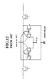
- Fig. 12 is a CMOS SRAM cell configured by prior-art thin film transistors.
- CMOS SRAM In manufacturing the CMOS SRAM, conventionally p-MOSFET and n-MOSFET are formed on a plane and connected to each other simply via an A l film pattern.
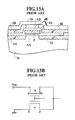
- a stacked CMOS structure To reduce the memory area of the CMOS SRAM, recently a stacked CMOS structure has been proposed, in which the CMOS can be formed by stacking polysilicon thin film transistors into three-dimentional form as shown in Fig. 13A.
- Fig. 13B is an equivalent circuit diagram corresponding to the stacked CMOS shown in Fig. 13A.
- the n-MOSFET is composed of n+-type silicon source and drain electrode layers 2A and 3A formed on a plane of a p-type single crystal silicon substrate 1a so as to form an active (channel forming) region AA in the silicon substrate 1a and between the source and drain electrodes 2A and 2B, a polysilicon common gate electrode 5 formed on the active region AA, and a silicon oxide gate insulating film 4A formed around the gate electrode 5 and on the active layer AA.
- the p-MOSFET (thin film transistor) stacked on the n-MOSFET is composed of p+-type polysilicon source and drain electrode layers 2B and 3B formed on the silicon oxide gate insulating film 4B so as to form another polysilicon active layer AB between the source and drain electrodes 2B and 3B and on the common gate electrode 5, and a protective insulating film 1b formed on the source and drain electrodes 2B and 3B.
- polysilicon gate electrode 5 is used in common for both the n- and p-MOSFETs.
- the CMOS SRAM shown in Fig. 12 can be formed by connecting these two CMOSFETs shown in Fig. 13.
- Fig. 14A shows a cross-sectional view of a stacked CMOS formed by the polysilicon thin film transistor according to the present invention as p-MOSFET
- Fig. 14B is an equivalent circuit diagram corresponding to the stacked CMOS shown in Fig. 14A.
- the drain electrode 3B of the p-MOSFET has a little offset away from the common gate electrode 5, and an additional subgate electrode 50 is formed on the offset active polysilicon layer AB by use of an A l film pattern, for instance.
- this subgate 50 serves effectively as p+-type drain electrode, so that it is possible to markedly reduce the p-MOSFET (thin film transistor) off current of the resulting in standby-power reduction of CMOSFET shown in Figs. 14A and 14B.
- Fig. 15A shows a cross-sectional view of another example of stacked CMOSs formed by polysilicon thin film transistor according to the present invention as p-MOSFET
- Fig. 15B is an equivalent circuit diagram corresponding to the stacked CMOS shown in Fig. 15A.
- the points different from the prior-art structure shown in Fig. 13A are that the drain electrode 3B of the p-MOSFET is a little offset away from the common gate electrode 5, and part of the source electrode 2A of the n-MOSFET is used in common as a subgate 50A formed under the offset active polysilicon layer AB.
- this subgate 50A serves effectively as a p+-type drain electrode, so that it is possible to markedly reduce the off current of the CMOSFETs shown in Figs. 15A and 15B.
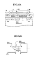
- Fig. 16A shows a cross-sectional view of another example of stacked CMOSs formed by two polysilicon thin film transistors according to the present invention
- Fig. 16B is an equivalent circuit diagram corresponding to the stacked CMOS shown in Fig. 16A.
- Fig. 13A The points different from the prior-art structure shown in Fig. 13A are that another gate 5A for the p-MOSFET is formed near the common electrode 5; and part of the source electrode 2A of the n-MOSFET is used in common as a subgate 50B formed under the middle active polysilicone layer AB between the two gate electrodes 5 and 5A.
- this subgate 50B serves effectively as an additional p+-type drain electrode, so that it is possible to markedly reduce the off current of the CMOSFETs shown in Figs. 16A and 16B.
- the power consumption can be improved when the SRAM is kept in the standby condition.
- Fig. 17 shows the drain current - gate voltage characteristics with the drain voltage kept at 10 V, in which the solid line shows the characteristics of the thin film transistor of the third embodiment (shown in Fig. 4 and an amorphous silicon film is used as the channel forming film) according to the present invention and the dashed line shows those of the prior-art amorphous silicon thin film transistor as shown in Fig. 1A.
- Fig. 17 indicates that the on current is almost the same in both, however, the off current of the amorphous silicon thin film transistor according to the present invention is as small as about 1/1000 or less as compared with that of the prior-art amorphous silicon thin film transistor.
- Fig. 18A shows the drain current - gate voltage characteristics with the drain voltage changed as parameter from 2.5 V to 20 V at a step of 2.5 V, for the prior-art polysilicon thin film transistor as shown in Fig. 1A.
- Fig. 18B shows the similar drain current - gate voltage characteristics with the drain voltage changed as parameter from 2.5 V to 20 V at a step of 2.5 V, for the thin film transistor of the third embodiment (shown in Fig. 4 and a polysilicon film is used as the channel forming film) according to the present invention.
- These graphs indicate that in the case of the prior-art polysilicon transistor, off current is high and further sharply increases with increasing negative gate voltage and with increasing positive drain voltage Vd.
- the off current of the polysilicon thin film transistor according to the present invention is as small as about 1/1000 or less at a gate voltage of -20 V and a drain voltage of 20 V. Additionally, it is possible to prevent the off current from being increased sharply with increasing positive drain voltage.
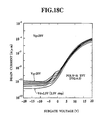
- Fig. 18C shows the drain current - subgate voltage characteristics with the drain voltage changed as parameter from 2.5 V to 20 V at a step of 2.5 V, for the thin film transistor of the third embodiment (shown in Fig. 4C and a polisilicon film is used as the channel forming film) according to the present invention, in which the first gate electrode 51 is replaced with the second and third gate electrodes 52 and 53. That is, in the case of Fig. 18C, a positive voltage is applied to the first (main) gate electrode 51 and a negative voltage is applied to the second and third (sub-) gate electrodes 52 and 53 to turn off the transistor. Fig. 18C also indicates that it is possible to markedly reduce the off current.
- n-p-n type transistors have mainly been described by way of example. Without being limited thereto, it is of course possible to apply the present invention to p-n-p type transistor. In this case, the n-type layer or region is replaced with the p-type layer or region or vice versa.
- the thin film transistor according to the present invention since at least one subgate is provided in addition to the main gate, in order to form (1) at least one pn drain junction induced by two opposite-polality electric fields in the channel forming region between the source and drain regions by applying a first voltage to the main gate and a second voltage opposite to the first voltage to the subgate or (2) at least thick depletion layers induced by two same-polarity different - intensity electric fields between the channel forming region and the source or drain region whenever the transistor is turned off, it is possible to markedly reduce the off current flowing between the source and drain regions in particular when a higher voltage is applied to the drain voltage and a higher negative voltage is applied to the main gate, without reducing the on current, thus markedly increasing the on/off current ratio of the thin film transistor.
- the thin film transistor can be used as in the same way as the ordinary three-terminal transistors.
- the thin film transistor can be formed in accordance with the ordinary transistor manufacturing process, without need of any special manufacturing steps, it is possible to improve the production yield and therefore manufacture the thin film transistor at low cost.
Landscapes
- Thin Film Transistor (AREA)
- Metal-Oxide And Bipolar Metal-Oxide Semiconductor Integrated Circuits (AREA)
Applications Claiming Priority (4)
| Application Number | Priority Date | Filing Date | Title |
|---|---|---|---|
| JP52409/90 | 1990-03-02 | ||
| JP5240990A JP2855155B2 (ja) | 1990-03-02 | 1990-03-02 | 薄膜トランジスタ |
| JP23020990A JP2869548B2 (ja) | 1990-08-31 | 1990-08-31 | 薄膜トランジスタ回路 |
| JP230209/90 | 1990-08-31 |
Publications (2)
| Publication Number | Publication Date |
|---|---|
| EP0444712A1 true EP0444712A1 (de) | 1991-09-04 |
| EP0444712B1 EP0444712B1 (de) | 1996-06-26 |
Family
ID=26393020
Family Applications (1)
| Application Number | Title | Priority Date | Filing Date |
|---|---|---|---|
| EP91103223A Expired - Lifetime EP0444712B1 (de) | 1990-03-02 | 1991-03-04 | Mehrfachgatter-Dünnfilmtransistor |
Country Status (4)
| Country | Link |
|---|---|
| US (1) | US5124769A (de) |
| EP (1) | EP0444712B1 (de) |
| KR (1) | KR940008262B1 (de) |
| DE (1) | DE69120440T2 (de) |
Cited By (8)
| Publication number | Priority date | Publication date | Assignee | Title |
|---|---|---|---|---|
| EP0570257A1 (de) * | 1992-05-15 | 1993-11-18 | Thomson-Csf | Feldeffekt-Halbleiteranordnung mit sekundärem Gate, Verfahren zur Herstellung und Verwendung in einer Matrix-Ansteuerungsanordnung |
| US6545328B1 (en) * | 1999-04-15 | 2003-04-08 | Sharp Kabushiki Kaisha | Semiconductor device |
| US6744082B1 (en) * | 2000-05-30 | 2004-06-01 | Micron Technology, Inc. | Static pass transistor logic with transistors with multiple vertical gates |
| EP1696480A3 (de) * | 2005-02-18 | 2009-07-29 | General Electric Company | Bauteil aus Freistehenden elektrostatisch dotierten Nanoröhrchen und Herstellungsverfahren dazu. |
| FR3004583A1 (fr) * | 2013-10-28 | 2014-10-17 | St Microelectronics Sa | Transistor mos a drain etendu en couche mince sur isolant |
| CN104241284A (zh) * | 2013-06-06 | 2014-12-24 | 旺宏电子股份有限公司 | 双模晶体管装置及其操作方法 |
| CN106783888A (zh) * | 2017-01-03 | 2017-05-31 | 京东方科技集团股份有限公司 | 显示屏及其控制方法、显示装置 |
| EP3982420A1 (de) * | 2020-10-08 | 2022-04-13 | Imec VZW | Dynamisch dotierter feldeffekttransistor und verfahren zu seiner steuerung |
Families Citing this family (49)
| Publication number | Priority date | Publication date | Assignee | Title |
|---|---|---|---|---|
| DE69128876T2 (de) * | 1990-11-30 | 1998-08-06 | Sharp Kk | Dünnfilm-Halbleitervorrichtung |
| JPH04241466A (ja) * | 1991-01-16 | 1992-08-28 | Casio Comput Co Ltd | 電界効果型トランジスタ |
| JP3255942B2 (ja) * | 1991-06-19 | 2002-02-12 | 株式会社半導体エネルギー研究所 | 逆スタガ薄膜トランジスタの作製方法 |
| JPH0590587A (ja) * | 1991-09-30 | 1993-04-09 | Sony Corp | 絶縁ゲート型電界効果トランジスタ |
| JPH0590586A (ja) * | 1991-09-30 | 1993-04-09 | Nec Corp | 薄膜トランジスタ |
| US5266515A (en) * | 1992-03-02 | 1993-11-30 | Motorola, Inc. | Fabricating dual gate thin film transistors |
| JP3254007B2 (ja) * | 1992-06-09 | 2002-02-04 | 株式会社半導体エネルギー研究所 | 薄膜状半導体装置およびその作製方法 |
| US5807772A (en) * | 1992-06-09 | 1998-09-15 | Semiconductor Energy Laboratory Co., Ltd. | Method for forming semiconductor device with bottom gate connected to source or drain |
| TW232751B (en) * | 1992-10-09 | 1994-10-21 | Semiconductor Energy Res Co Ltd | Semiconductor device and method for forming the same |
| US6624477B1 (en) | 1992-10-09 | 2003-09-23 | Semiconductor Energy Laboratory Co., Ltd. | Semiconductor device and method for manufacturing the same |
| JP3369244B2 (ja) * | 1993-03-12 | 2003-01-20 | 株式会社半導体エネルギー研究所 | 薄膜トランジスタ |
| JP3637069B2 (ja) | 1993-03-12 | 2005-04-06 | 株式会社半導体エネルギー研究所 | 半導体装置の作製方法 |
| US5569936A (en) * | 1993-03-12 | 1996-10-29 | Semiconductor Energy Laboratory Co., Ltd. | Semiconductor device employing crystallization catalyst |
| CN1542929B (zh) * | 1993-03-12 | 2012-05-30 | 株式会社半导体能源研究所 | 半导体器件的制造方法 |
| KR960012585B1 (en) * | 1993-06-25 | 1996-09-23 | Samsung Electronics Co Ltd | Transistor structure and the method for manufacturing the same |
| GB9325984D0 (en) * | 1993-12-20 | 1994-02-23 | Philips Electronics Uk Ltd | Manufacture of electronic devices comprising thin-film transistors |
| JPH07302912A (ja) * | 1994-04-29 | 1995-11-14 | Semiconductor Energy Lab Co Ltd | 半導体装置 |
| US5804837A (en) * | 1994-06-27 | 1998-09-08 | Samsung Electronics Co., Ltd. | Polysilicon thin-film transistor and method for fabricating the same |
| KR0151195B1 (ko) * | 1994-09-13 | 1998-10-01 | 문정환 | 박막 트랜지스터의 구조 및 제조방법 |
| US5670399A (en) * | 1995-12-06 | 1997-09-23 | Micron Technology, Inc. | Method of making thin film transistor with offset drain |
| US5648671A (en) * | 1995-12-13 | 1997-07-15 | U S Philips Corporation | Lateral thin-film SOI devices with linearly-graded field oxide and linear doping profile |
| KR0177785B1 (ko) * | 1996-02-03 | 1999-03-20 | 김광호 | 오프셋 구조를 가지는 트랜지스터 및 그 제조방법 |
| US5920085A (en) * | 1996-02-03 | 1999-07-06 | Samsung Electronics Co., Ltd. | Multiple floating gate field effect transistors and methods of operating same |
| KR100219117B1 (ko) * | 1996-08-24 | 1999-09-01 | 구자홍 | 박막트랜지스터 액정표시장치 및 그 제조방법 |
| US5953596A (en) * | 1996-12-19 | 1999-09-14 | Micron Technology, Inc. | Methods of forming thin film transistors |
| JP3391717B2 (ja) * | 1997-12-24 | 2003-03-31 | シャープ株式会社 | 反射型液晶表示装置 |
| JP4076648B2 (ja) | 1998-12-18 | 2008-04-16 | 株式会社半導体エネルギー研究所 | 半導体装置 |
| JP4008133B2 (ja) * | 1998-12-25 | 2007-11-14 | 株式会社半導体エネルギー研究所 | 半導体装置 |
| JP4202502B2 (ja) | 1998-12-28 | 2008-12-24 | 株式会社半導体エネルギー研究所 | 半導体装置 |
| US8158980B2 (en) | 2001-04-19 | 2012-04-17 | Semiconductor Energy Laboratory Co., Ltd. | Semiconductor device having a pixel matrix circuit that includes a pixel TFT and a storage capacitor |
| TWI246755B (en) * | 2001-01-29 | 2006-01-01 | Seiko Epson Corp | Semiconductor device, circuit board, electro-optical device, and electronic apparatus |
| JP4443063B2 (ja) * | 2001-02-28 | 2010-03-31 | 株式会社日立製作所 | 電界効果トランジスタ及びそれを使用した画像表示装置 |
| US20060007772A1 (en) * | 2002-03-19 | 2006-01-12 | O2Ic, Inc. | Non-volatile memory device |
| AU2002246316A1 (en) * | 2002-04-08 | 2003-10-27 | Council Of Scientific And Industrial Research | Process for the production of neodymium-iron-boron permanent magnet alloy powder |
| US7541614B2 (en) | 2003-03-11 | 2009-06-02 | Semiconductor Energy Laboratory Co., Ltd. | Integrated circuit, semiconductor device comprising the same, electronic device having the same, and driving method of the same |
| US20060081936A1 (en) * | 2004-09-28 | 2006-04-20 | Jae-Joon Kim | Semiconductor device for low power operation |
| KR101100426B1 (ko) * | 2005-05-10 | 2011-12-30 | 삼성전자주식회사 | 단결정 실리콘층을 포함하는 반도체 소자, 이를 포함하는반도체 장치 및 평면표시장치와 반도체 소자의 제조 방법 |
| US7459755B2 (en) * | 2006-05-25 | 2008-12-02 | Walker Andrew J | Dual-gate semiconductor devices with enhanced scalability |
| KR20110037220A (ko) * | 2009-10-06 | 2011-04-13 | 삼성모바일디스플레이주식회사 | 박막 트랜지스터, 그의 제조 방법 및 박막 트랜지스터를 구비하는 유기전계발광 표시 장치 |
| KR101056229B1 (ko) * | 2009-10-12 | 2011-08-11 | 삼성모바일디스플레이주식회사 | 박막 트랜지스터, 그의 제조 방법 및 박막 트랜지스터를 구비하는 유기전계발광 표시 장치 |
| WO2014170949A1 (ja) | 2013-04-16 | 2014-10-23 | ユニサンティス エレクトロニクス シンガポール プライベート リミテッド | 半導体装置の製造方法、及び、半導体装置 |
| KR102194235B1 (ko) * | 2013-09-05 | 2020-12-22 | 삼성전자주식회사 | 박막 트랜지스터 및 그 구동 방법 |
| US9299848B2 (en) * | 2014-03-14 | 2016-03-29 | Semiconductor Energy Laboratory Co., Ltd. | Semiconductor device, RF tag, and electronic device |
| KR102329267B1 (ko) * | 2014-09-29 | 2021-11-22 | 삼성디스플레이 주식회사 | 박막트랜지스터 기판, 이를 구비한 디스플레이 장치, 박막트랜지스터 기판 제조방법 및 디스플레이 장치 제조방법 |
| CN109037240B (zh) * | 2018-07-27 | 2020-11-10 | 京东方科技集团股份有限公司 | 阵列基板及其制作方法、显示面板、显示装置 |
| TWI695205B (zh) * | 2018-08-10 | 2020-06-01 | 友達光電股份有限公司 | 影像感測顯示裝置以及影像處理方法 |
| CN111987112B (zh) * | 2019-05-22 | 2024-07-05 | 群创光电股份有限公司 | 放射线感测装置 |
| US11393820B2 (en) * | 2020-10-26 | 2022-07-19 | Micron Technology, Inc. | Vertical digit line for semiconductor devices |
| KR102891376B1 (ko) * | 2020-12-14 | 2025-11-25 | 엘지디스플레이 주식회사 | 박막 트랜지스터 및 이를 포함하는 표시장치 |
Citations (5)
| Publication number | Priority date | Publication date | Assignee | Title |
|---|---|---|---|---|
| FR1505959A (fr) * | 1965-12-22 | 1967-12-15 | Philips Nv | Dispositif semi-conducteur |
| DE1514362B1 (de) * | 1964-07-31 | 1970-10-22 | Rca Corp | Feldeffekttransistor |
| US4065781A (en) * | 1974-06-21 | 1977-12-27 | Westinghouse Electric Corporation | Insulated-gate thin film transistor with low leakage current |
| EP0066675A1 (de) * | 1981-06-08 | 1982-12-15 | International Business Machines Corporation | Verfahren zur Herstellung der Feldeffekttransistoren |
| EP0166261A2 (de) * | 1984-06-27 | 1986-01-02 | Energy Conversion Devices, Inc. | Statisches Feld induzierte Halbleiteranordnungen |
Family Cites Families (7)
| Publication number | Priority date | Publication date | Assignee | Title |
|---|---|---|---|---|
| JPS57121277A (en) * | 1981-01-21 | 1982-07-28 | Hitachi Ltd | Semiconductor device and manufacture thereof |
| JPS58107676A (ja) * | 1981-12-21 | 1983-06-27 | Nec Corp | 半導体装置 |
| JPS6188565A (ja) * | 1984-10-05 | 1986-05-06 | Sony Corp | 電界効果型トランジスタ |
| US5012315A (en) * | 1989-01-09 | 1991-04-30 | Regents Of University Of Minnesota | Split-gate field effect transistor |
| US4984040A (en) * | 1989-06-15 | 1991-01-08 | Xerox Corporation | High voltage thin film transistor with second gate |
| US4984041A (en) * | 1989-07-28 | 1991-01-08 | Xerox Corporation | High voltage thin film transistor with second control electrode |
| US5017983A (en) * | 1989-08-03 | 1991-05-21 | Industrial Technology Research Institute | Amorphous silicon thin film transistor with a depletion gate |
-
1991
- 1991-03-01 US US07/663,372 patent/US5124769A/en not_active Expired - Lifetime
- 1991-03-02 KR KR1019910003499A patent/KR940008262B1/ko not_active Expired - Fee Related
- 1991-03-04 EP EP91103223A patent/EP0444712B1/de not_active Expired - Lifetime
- 1991-03-04 DE DE69120440T patent/DE69120440T2/de not_active Expired - Fee Related
Patent Citations (5)
| Publication number | Priority date | Publication date | Assignee | Title |
|---|---|---|---|---|
| DE1514362B1 (de) * | 1964-07-31 | 1970-10-22 | Rca Corp | Feldeffekttransistor |
| FR1505959A (fr) * | 1965-12-22 | 1967-12-15 | Philips Nv | Dispositif semi-conducteur |
| US4065781A (en) * | 1974-06-21 | 1977-12-27 | Westinghouse Electric Corporation | Insulated-gate thin film transistor with low leakage current |
| EP0066675A1 (de) * | 1981-06-08 | 1982-12-15 | International Business Machines Corporation | Verfahren zur Herstellung der Feldeffekttransistoren |
| EP0166261A2 (de) * | 1984-06-27 | 1986-01-02 | Energy Conversion Devices, Inc. | Statisches Feld induzierte Halbleiteranordnungen |
Non-Patent Citations (5)
| Title |
|---|
| INTERNATIONAL JOURNAL OF ELECTRONICS. vol. 54, no. 2, February 1983, LONDON GB pages 287 - 298; K. V. ANAND et al: "A novel p-n junction polycrystalline silicon gate MOSFET" * |
| PATENT ABSTRACTS OF JAPAN vol. 10, no. 263 (E-435)(2319) 09 September 1986, & JP-A-61 88565 (SONY CORP) 06 May 1986, * |
| PATENT ABSTRACTS OF JAPAN vol. 6, no. 218 (E-139)(1096) 02 November 1982, & JP-A-57 121277 (HITACHI SEISAKUSHO K.K.) 28 July 1982, * |
| PATENT ABSTRACTS OF JAPAN vol. 7, no. 214 (E-199)(1359) 21 September 1983, & JP-A-58 107676 (NIPPON DENKI K.K.) 27 June 1983, * |
| PROCEEDINGS OF THE IEEE. vol. 55, no. 7, July 1967, NEW YORK US pages 1217 - 1218; R. G. WAGNER et al: "A Dual Offset Gate Thin-Film Transistor" * |
Cited By (14)
| Publication number | Priority date | Publication date | Assignee | Title |
|---|---|---|---|---|
| EP0570257A1 (de) * | 1992-05-15 | 1993-11-18 | Thomson-Csf | Feldeffekt-Halbleiteranordnung mit sekundärem Gate, Verfahren zur Herstellung und Verwendung in einer Matrix-Ansteuerungsanordnung |
| FR2691289A1 (fr) * | 1992-05-15 | 1993-11-19 | Thomson Csf | Dispositif semiconducteur à effet de champ, procédé de réalisation et application à un dispositif à commande matricielle. |
| US6545328B1 (en) * | 1999-04-15 | 2003-04-08 | Sharp Kabushiki Kaisha | Semiconductor device |
| US6744082B1 (en) * | 2000-05-30 | 2004-06-01 | Micron Technology, Inc. | Static pass transistor logic with transistors with multiple vertical gates |
| US6991988B2 (en) | 2000-05-30 | 2006-01-31 | Micron Technology, Inc. | Static pass transistor logic with transistors with multiple vertical gates |
| EP1696480A3 (de) * | 2005-02-18 | 2009-07-29 | General Electric Company | Bauteil aus Freistehenden elektrostatisch dotierten Nanoröhrchen und Herstellungsverfahren dazu. |
| CN104241284B (zh) * | 2013-06-06 | 2017-05-17 | 旺宏电子股份有限公司 | 双模晶体管装置及其操作方法 |
| CN104241284A (zh) * | 2013-06-06 | 2014-12-24 | 旺宏电子股份有限公司 | 双模晶体管装置及其操作方法 |
| US9373714B2 (en) | 2013-10-28 | 2016-06-21 | Stmicroelectronics Sa | Extended-drain MOS transistor in a thin film on insulator |
| FR3004583A1 (fr) * | 2013-10-28 | 2014-10-17 | St Microelectronics Sa | Transistor mos a drain etendu en couche mince sur isolant |
| CN106783888A (zh) * | 2017-01-03 | 2017-05-31 | 京东方科技集团股份有限公司 | 显示屏及其控制方法、显示装置 |
| CN106783888B (zh) * | 2017-01-03 | 2020-06-30 | 京东方科技集团股份有限公司 | 显示屏及其控制方法、显示装置 |
| EP3982420A1 (de) * | 2020-10-08 | 2022-04-13 | Imec VZW | Dynamisch dotierter feldeffekttransistor und verfahren zu seiner steuerung |
| US12154979B2 (en) | 2020-10-08 | 2024-11-26 | Imec Vzw | Dynamically doped field-effect transistor and a method for controlling such |
Also Published As
| Publication number | Publication date |
|---|---|
| KR910017674A (ko) | 1991-11-05 |
| KR940008262B1 (ko) | 1994-09-09 |
| DE69120440D1 (de) | 1996-08-01 |
| US5124769A (en) | 1992-06-23 |
| EP0444712B1 (de) | 1996-06-26 |
| DE69120440T2 (de) | 1997-01-09 |
Similar Documents
| Publication | Publication Date | Title |
|---|---|---|
| US5124769A (en) | Thin film transistor | |
| US5808344A (en) | Single-transistor logic and CMOS inverters | |
| US5894157A (en) | MOS transistor having an offset resistance derived from a multiple region gate electrode | |
| US5523603A (en) | Semiconductor device with reduced time-dependent dielectric failures | |
| US6049110A (en) | Body driven SOI-MOS field effect transistor | |
| US5616944A (en) | Diode and semiconductor device having a controlled intrinsic or low impurity concentration region between opposite conductivity type semiconductor regions | |
| EP0564204A2 (de) | Halbleiteranordnung | |
| US5341009A (en) | Fast charging MOS capacitor structure for high magnitude voltage of either positive or negative polarity | |
| JPH02122665A (ja) | 電源バッテリの極性の反転に対して自己保護されている集積回路 | |
| US4084108A (en) | Integrated circuit device | |
| US5914513A (en) | Electronically tunable capacitor | |
| US20010015449A1 (en) | Semiconductor - oxide - semiconductor capacitor formed in intergtated circuit | |
| US3639813A (en) | Complementary enhancement and depletion mosfets with common gate and channel region, the depletion mosfet also being a jfet | |
| US4216490A (en) | Static induction transistor | |
| EP0480500B1 (de) | Feldeffekttransistor mit verteilter Schwellenspannung | |
| US5602410A (en) | Off-state gate-oxide field reduction in CMOS | |
| JPH025302B2 (de) | ||
| KR100540404B1 (ko) | 반도체 장치 | |
| JP2869548B2 (ja) | 薄膜トランジスタ回路 | |
| US3757145A (en) | Integrable igfet circuit | |
| EP0093557B1 (de) | Schnelle integrierte komplementäre Halbleiterschaltung | |
| KR0136384B1 (ko) | 반도체 소자 | |
| US12628413B2 (en) | Semiconductor device | |
| JPH01227478A (ja) | 半導体装置 | |
| JPS6110992B2 (de) |
Legal Events
| Date | Code | Title | Description |
|---|---|---|---|
| PUAI | Public reference made under article 153(3) epc to a published international application that has entered the european phase |
Free format text: ORIGINAL CODE: 0009012 |
|
| 17P | Request for examination filed |
Effective date: 19910304 |
|
| AK | Designated contracting states |
Kind code of ref document: A1 Designated state(s): DE FR GB |
|
| 17Q | First examination report despatched |
Effective date: 19930623 |
|
| RAP1 | Party data changed (applicant data changed or rights of an application transferred) |
Owner name: NIPPON TELEGRAPH AND TELEPHONE CORPORATION |
|
| GRAA | (expected) grant |
Free format text: ORIGINAL CODE: 0009210 |
|
| AK | Designated contracting states |
Kind code of ref document: B1 Designated state(s): DE FR GB |
|
| REF | Corresponds to: |
Ref document number: 69120440 Country of ref document: DE Date of ref document: 19960801 |
|
| ET | Fr: translation filed | ||
| PLBE | No opposition filed within time limit |
Free format text: ORIGINAL CODE: 0009261 |
|
| STAA | Information on the status of an ep patent application or granted ep patent |
Free format text: STATUS: NO OPPOSITION FILED WITHIN TIME LIMIT |
|
| 26N | No opposition filed | ||
| REG | Reference to a national code |
Ref country code: GB Ref legal event code: IF02 |
|
| PGFP | Annual fee paid to national office [announced via postgrant information from national office to epo] |
Ref country code: GB Payment date: 20080312 Year of fee payment: 18 |
|
| PGFP | Annual fee paid to national office [announced via postgrant information from national office to epo] |
Ref country code: FR Payment date: 20080214 Year of fee payment: 18 Ref country code: DE Payment date: 20080422 Year of fee payment: 18 |
|
| GBPC | Gb: european patent ceased through non-payment of renewal fee |
Effective date: 20090304 |
|
| REG | Reference to a national code |
Ref country code: FR Ref legal event code: ST Effective date: 20091130 |
|
| PG25 | Lapsed in a contracting state [announced via postgrant information from national office to epo] |
Ref country code: DE Free format text: LAPSE BECAUSE OF NON-PAYMENT OF DUE FEES Effective date: 20091001 |
|
| PG25 | Lapsed in a contracting state [announced via postgrant information from national office to epo] |
Ref country code: GB Free format text: LAPSE BECAUSE OF NON-PAYMENT OF DUE FEES Effective date: 20090304 Ref country code: FR Free format text: LAPSE BECAUSE OF NON-PAYMENT OF DUE FEES Effective date: 20091123 |