EP0570257A1 - Feldeffekt-Halbleiteranordnung mit sekundärem Gate, Verfahren zur Herstellung und Verwendung in einer Matrix-Ansteuerungsanordnung - Google Patents
Feldeffekt-Halbleiteranordnung mit sekundärem Gate, Verfahren zur Herstellung und Verwendung in einer Matrix-Ansteuerungsanordnung Download PDFInfo
- Publication number
- EP0570257A1 EP0570257A1 EP19930401148 EP93401148A EP0570257A1 EP 0570257 A1 EP0570257 A1 EP 0570257A1 EP 19930401148 EP19930401148 EP 19930401148 EP 93401148 A EP93401148 A EP 93401148A EP 0570257 A1 EP0570257 A1 EP 0570257A1
- Authority
- EP
- European Patent Office
- Prior art keywords
- drain
- channel
- source
- grid
- layer
- Prior art date
- Legal status (The legal status is an assumption and is not a legal conclusion. Google has not performed a legal analysis and makes no representation as to the accuracy of the status listed.)
- Withdrawn
Links
- 239000004065 semiconductor Substances 0.000 title claims abstract description 45
- 230000005669 field effect Effects 0.000 title claims abstract description 23
- 239000011159 matrix material Substances 0.000 title claims abstract description 9
- 238000000034 method Methods 0.000 title claims description 11
- 230000008569 process Effects 0.000 title description 3
- 238000004519 manufacturing process Methods 0.000 claims abstract description 17
- 230000010287 polarization Effects 0.000 claims abstract description 9
- 239000000758 substrate Substances 0.000 claims description 22
- 239000000463 material Substances 0.000 claims description 19
- 101100484930 Saccharomyces cerevisiae (strain ATCC 204508 / S288c) VPS41 gene Proteins 0.000 claims description 18
- 238000002513 implantation Methods 0.000 claims description 14
- 239000004020 conductor Substances 0.000 claims description 11
- 238000005468 ion implantation Methods 0.000 claims description 11
- 238000009413 insulation Methods 0.000 claims description 10
- 238000005530 etching Methods 0.000 claims description 9
- 239000011347 resin Substances 0.000 claims description 9
- 229920005989 resin Polymers 0.000 claims description 9
- 238000000151 deposition Methods 0.000 claims description 7
- 230000000694 effects Effects 0.000 claims description 4
- 239000011810 insulating material Substances 0.000 claims description 4
- 230000008021 deposition Effects 0.000 claims description 3
- 239000003989 dielectric material Substances 0.000 claims description 3
- 238000009825 accumulation Methods 0.000 abstract description 7
- 108091006146 Channels Proteins 0.000 description 30
- XUIMIQQOPSSXEZ-UHFFFAOYSA-N Silicon Chemical compound [Si] XUIMIQQOPSSXEZ-UHFFFAOYSA-N 0.000 description 22
- VYPSYNLAJGMNEJ-UHFFFAOYSA-N silicon dioxide Inorganic materials O=[Si]=O VYPSYNLAJGMNEJ-UHFFFAOYSA-N 0.000 description 20
- 229910052710 silicon Inorganic materials 0.000 description 13
- 239000010703 silicon Substances 0.000 description 13
- 229910052581 Si3N4 Inorganic materials 0.000 description 11
- 235000012239 silicon dioxide Nutrition 0.000 description 11
- 229910052681 coesite Inorganic materials 0.000 description 9
- 229910052906 cristobalite Inorganic materials 0.000 description 9
- 229910052751 metal Inorganic materials 0.000 description 9
- 239000002184 metal Substances 0.000 description 9
- 239000000377 silicon dioxide Substances 0.000 description 9
- 229910052682 stishovite Inorganic materials 0.000 description 9
- 229910052905 tridymite Inorganic materials 0.000 description 9
- 229910052782 aluminium Inorganic materials 0.000 description 8
- XAGFODPZIPBFFR-UHFFFAOYSA-N aluminium Chemical compound [Al] XAGFODPZIPBFFR-UHFFFAOYSA-N 0.000 description 8
- 229910021420 polycrystalline silicon Inorganic materials 0.000 description 8
- 239000005380 borophosphosilicate glass Substances 0.000 description 6
- 230000005684 electric field Effects 0.000 description 6
- 238000000137 annealing Methods 0.000 description 5
- 239000004411 aluminium Substances 0.000 description 4
- 238000005516 engineering process Methods 0.000 description 4
- 238000000623 plasma-assisted chemical vapour deposition Methods 0.000 description 4
- 230000000903 blocking effect Effects 0.000 description 3
- 230000007547 defect Effects 0.000 description 3
- 239000011521 glass Substances 0.000 description 3
- 238000007254 oxidation reaction Methods 0.000 description 3
- 230000004913 activation Effects 0.000 description 2
- QVGXLLKOCUKJST-UHFFFAOYSA-N atomic oxygen Chemical compound [O] QVGXLLKOCUKJST-UHFFFAOYSA-N 0.000 description 2
- 230000015572 biosynthetic process Effects 0.000 description 2
- 239000002019 doping agent Substances 0.000 description 2
- 238000002347 injection Methods 0.000 description 2
- 239000007924 injection Substances 0.000 description 2
- 239000012212 insulator Substances 0.000 description 2
- 239000004973 liquid crystal related substance Substances 0.000 description 2
- 238000011068 loading method Methods 0.000 description 2
- 230000007246 mechanism Effects 0.000 description 2
- 238000001465 metallisation Methods 0.000 description 2
- 230000003647 oxidation Effects 0.000 description 2
- 229910052760 oxygen Inorganic materials 0.000 description 2
- 239000001301 oxygen Substances 0.000 description 2
- 229920005591 polysilicon Polymers 0.000 description 2
- 239000010453 quartz Substances 0.000 description 2
- 230000009467 reduction Effects 0.000 description 2
- 229910052594 sapphire Inorganic materials 0.000 description 2
- 239000010980 sapphire Substances 0.000 description 2
- 238000000926 separation method Methods 0.000 description 2
- 206010019345 Heat stroke Diseases 0.000 description 1
- 102000004129 N-Type Calcium Channels Human genes 0.000 description 1
- 108090000699 N-Type Calcium Channels Proteins 0.000 description 1
- 208000007180 Sunstroke Diseases 0.000 description 1
- 241001639412 Verres Species 0.000 description 1
- 240000008042 Zea mays Species 0.000 description 1
- 230000002745 absorbent Effects 0.000 description 1
- 239000002250 absorbent Substances 0.000 description 1
- 239000000969 carrier Substances 0.000 description 1
- 230000008859 change Effects 0.000 description 1
- 229940082150 encore Drugs 0.000 description 1
- 238000010438 heat treatment Methods 0.000 description 1
- 238000002955 isolation Methods 0.000 description 1
- 230000000873 masking effect Effects 0.000 description 1
- 229910021421 monocrystalline silicon Inorganic materials 0.000 description 1
- 238000002161 passivation Methods 0.000 description 1
- 239000007787 solid Substances 0.000 description 1
- 230000007704 transition Effects 0.000 description 1
Images


Classifications
-
- H—ELECTRICITY
- H10—SEMICONDUCTOR DEVICES; ELECTRIC SOLID-STATE DEVICES NOT OTHERWISE PROVIDED FOR
- H10D—INORGANIC ELECTRIC SEMICONDUCTOR DEVICES
- H10D62/00—Semiconductor bodies, or regions thereof, of devices having potential barriers
- H10D62/10—Shapes, relative sizes or dispositions of the regions of the semiconductor bodies; Shapes of the semiconductor bodies
- H10D62/13—Semiconductor regions connected to electrodes carrying current to be rectified, amplified or switched, e.g. source or drain regions
- H10D62/149—Source or drain regions of field-effect devices
- H10D62/151—Source or drain regions of field-effect devices of IGFETs
-
- H—ELECTRICITY
- H10—SEMICONDUCTOR DEVICES; ELECTRIC SOLID-STATE DEVICES NOT OTHERWISE PROVIDED FOR
- H10D—INORGANIC ELECTRIC SEMICONDUCTOR DEVICES
- H10D30/00—Field-effect transistors [FET]
- H10D30/01—Manufacture or treatment
- H10D30/021—Manufacture or treatment of FETs having insulated gates [IGFET]
- H10D30/031—Manufacture or treatment of FETs having insulated gates [IGFET] of thin-film transistors [TFT]
- H10D30/0321—Manufacture or treatment of FETs having insulated gates [IGFET] of thin-film transistors [TFT] comprising silicon, e.g. amorphous silicon or polysilicon
- H10D30/0323—Manufacture or treatment of FETs having insulated gates [IGFET] of thin-film transistors [TFT] comprising silicon, e.g. amorphous silicon or polysilicon comprising monocrystalline silicon
- H10D30/0327—Manufacture or treatment of FETs having insulated gates [IGFET] of thin-film transistors [TFT] comprising silicon, e.g. amorphous silicon or polysilicon comprising monocrystalline silicon on sapphire substrates, e.g. of silicon-on-sapphire [SOS] transistor
-
- H—ELECTRICITY
- H10—SEMICONDUCTOR DEVICES; ELECTRIC SOLID-STATE DEVICES NOT OTHERWISE PROVIDED FOR
- H10D—INORGANIC ELECTRIC SEMICONDUCTOR DEVICES
- H10D30/00—Field-effect transistors [FET]
- H10D30/60—Insulated-gate field-effect transistors [IGFET]
- H10D30/67—Thin-film transistors [TFT]
- H10D30/6704—Thin-film transistors [TFT] having supplementary regions or layers in the thin films or in the insulated bulk substrates for controlling properties of the device
- H10D30/6713—Thin-film transistors [TFT] having supplementary regions or layers in the thin films or in the insulated bulk substrates for controlling properties of the device characterised by the properties of the source or drain regions, e.g. compositions or sectional shapes
- H10D30/6715—Thin-film transistors [TFT] having supplementary regions or layers in the thin films or in the insulated bulk substrates for controlling properties of the device characterised by the properties of the source or drain regions, e.g. compositions or sectional shapes characterised by the doping profiles, e.g. having lightly-doped source or drain extensions
-
- H—ELECTRICITY
- H10—SEMICONDUCTOR DEVICES; ELECTRIC SOLID-STATE DEVICES NOT OTHERWISE PROVIDED FOR
- H10D—INORGANIC ELECTRIC SEMICONDUCTOR DEVICES
- H10D30/00—Field-effect transistors [FET]
- H10D30/60—Insulated-gate field-effect transistors [IGFET]
- H10D30/67—Thin-film transistors [TFT]
- H10D30/6729—Thin-film transistors [TFT] characterised by the electrodes
- H10D30/673—Thin-film transistors [TFT] characterised by the electrodes characterised by the shapes, relative sizes or dispositions of the gate electrodes
- H10D30/6733—Multi-gate TFTs
- H10D30/6734—Multi-gate TFTs having gate electrodes arranged on both top and bottom sides of the channel, e.g. dual-gate TFTs
-
- H—ELECTRICITY
- H10—SEMICONDUCTOR DEVICES; ELECTRIC SOLID-STATE DEVICES NOT OTHERWISE PROVIDED FOR
- H10D—INORGANIC ELECTRIC SEMICONDUCTOR DEVICES
- H10D30/00—Field-effect transistors [FET]
- H10D30/60—Insulated-gate field-effect transistors [IGFET]
- H10D30/68—Floating-gate IGFETs
-
- G—PHYSICS
- G02—OPTICS
- G02F—OPTICAL DEVICES OR ARRANGEMENTS FOR THE CONTROL OF LIGHT BY MODIFICATION OF THE OPTICAL PROPERTIES OF THE MEDIA OF THE ELEMENTS INVOLVED THEREIN; NON-LINEAR OPTICS; FREQUENCY-CHANGING OF LIGHT; OPTICAL LOGIC ELEMENTS; OPTICAL ANALOGUE/DIGITAL CONVERTERS
- G02F1/00—Devices or arrangements for the control of the intensity, colour, phase, polarisation or direction of light arriving from an independent light source, e.g. switching, gating or modulating; Non-linear optics
- G02F1/01—Devices or arrangements for the control of the intensity, colour, phase, polarisation or direction of light arriving from an independent light source, e.g. switching, gating or modulating; Non-linear optics for the control of the intensity, phase, polarisation or colour
- G02F1/13—Devices or arrangements for the control of the intensity, colour, phase, polarisation or direction of light arriving from an independent light source, e.g. switching, gating or modulating; Non-linear optics for the control of the intensity, phase, polarisation or colour based on liquid crystals, e.g. single liquid crystal display cells
- G02F1/133—Constructional arrangements; Operation of liquid crystal cells; Circuit arrangements
- G02F1/136—Liquid crystal cells structurally associated with a semi-conducting layer or substrate, e.g. cells forming part of an integrated circuit
- G02F1/1362—Active matrix addressed cells
- G02F1/1368—Active matrix addressed cells in which the switching element is a three-electrode device
Definitions
- the invention relates to a field effect semiconductor device and more particularly to a field effect transistor of the MOS (Metal / Oxide / Semiconductor) type manufactured in monocrystalline or polycrystalline silicon on insulator. It also relates to a method for producing this device and to an application to a device with matrix control.
- MOS Metal / Oxide / Semiconductor
- the proposed structure reduces leakage currents in the blocking state.
- the invention can advantageously be applied to transistors based on polycrystalline silicon, and in particular to those intended to be used for controlling the pixels of flat screens with liquid crystal and active matrix.
- FIG. 1 represents a network of transfer characteristics typical of an MOS-type transistor with an n-type channel made from polycrystalline silicon deposited on a glass or quartz substrate.
- FIGS. 2a to 2d illustrate a structure of a field effect transistor known in the art and its different conduction states.
- a field effect transistor known in the art and its different conduction states.
- Such a transistor has, in a p-type semiconductor substrate, two n++-type doped zones. These zones of type n++ take the place of drain D and source S and are therefore separated by a zone of type p. Above this p-type zone is located a layer IS insulation on which a metal gate G electrode is located.
- FIGS. 2a and 2b the application of a positive voltage on the grid induces the formation of an inversion layer in the channel, the reference of the voltages being the source which is connected to earth; the transistor is on.
- FIGS. 2c and 2d the case is shown where the gate voltage is negative, which induces the formation of an accumulation layer in the channel.
- the drain-source structure consists of two head-to-tail junctions and the transistor is blocking.
- the source and drain contact regions are produced by ion implantation, possibly self-aligned by the grid.
- the heat treatment temperatures oxidation, implantation annealing, etc.
- the heat treatment temperatures are always kept low ( ⁇ 950 ° C. for refractory insulating substrates such as sapphire, quartz or silicon oxidized and ⁇ 600 ° C for glass substrates) for complex reasons of multiplication of defects, change of type of the deposited silicon or quite simply of softening of the substrate.
- the implantation annealing is imperfect, which leads to the generation of deep levels in the gap of the semiconductor.
- FIG. 3a shows the strip structure of the semiconductor with deep levels located in the middle of the gap.
- a band of deep levels DF has been represented, the introduction of which will be assumed to follow an annealing of imperfect implantation.
- FIG. 3b a reverse-polarized drain-channel type junction is shown (situation described in FIGS. 2c and 2d); it is found qualitatively that the higher the reverse polarization (therefore the higher the electric field), the higher the probability of tunnel effect assisted by faults through the junction.
- the electric field can be reduced by performing a gradual doping on the drain side, so as to obtain a structure called LDD (Ligthly Doped Drain).
- LDD Ligthly Doped Drain
- the effectiveness of this type of structure, shown in Figure 4 has been demonstrated in particular by Keiji NAKAZAWA and Collaborators in an article published in "Society of Information Display 1990 Digest", p. 311.
- the drawback, however, of this type of structure lies in the reduction in the current of the transistors in the on state (reduction of 1 to 2 orders of magnitude) due to the effect of series resistance due to the weakly doped region.
- a second approach can be used, which consists in deporting the drain-channel junction outside the region where the ion implantation takes place.
- the present invention avoids the use of a fourth electrode as well as the use of a secondary drain-gate link. It also makes it possible to obtain a transistor passing for any positive value of gate voltage (in the case of an n-channel transistor as shown in FIGS. 2a and 2c).
- the invention relates to a field effect semiconductor device comprising a source zone and a drain zone of doped semiconductor material of a first type and separated by a channel of intrinsic or doped semiconductor material of a second type, characterized in that that it involves minus a secondary grid, without external connection electrically charged to a substantially determined floating level, this secondary grid being located in a plane parallel to the channel and facing the latter.
- the invention relates to a field effect device comprising a source zone and a drain zone of doped semiconductor material of a first type separated by a channel of doped semiconductor material of a second type or intrinsic, of which the conduction state is controlled by a main grid, characterized in that it comprises at least one secondary grid electrically charged at a substantially determined floating level or else comprising a controlled density of fixed charges, this grid being located in a parallel plane at the canal, facing the canal and isolated from it, and near the drain.
- the invention also relates to a method for producing a field effect transistor, characterized in that it comprises the production on a substrate of a layer of semiconductor material comprising two source and drain regions doped of a type determined connected by a doped channel of another type or intrinsic and of two secondary grids located above the channel, each near a source or drain area and then a main gate located in an area whose projection in the plane of the channel is substantially between the secondary grids; the source-channel junction on the drain-channel junction or the two junctions then being strongly polarized temporarily in reverse, so as to come to charge the floating secondary grids, by injection of carriers through the insulating dielectric.
- the principle of the invention consists in providing on either side of the channel of the field effect transistor two permanent inversion or accumulation zones. This can be done using appropriate charges injected on two floating secondary grids placed on either side of the channel, or using charges injected at the interface between two dielectric layers (for example Si3N4 and SiO2 ) also arranged on either side of the channel, or even using charges trapped in a single dielectric comprising two branches always arranged on either side of the channel.
- two dielectric layers for example Si3N4 and SiO2
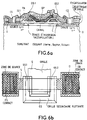
- Figures 6a and 6b show an exemplary embodiment of a transistor structure according to the invention in the case where the channel is bordered on either side by two floating secondary gates.
- FIG. 6a represents in section a transistor according to the invention in which a source zone S and a zone of drain D of doped semiconductor material of a determined type are implanted on a substrate. These zones are connected by a channel C made of doped semiconductor material of another type or else intrinsic. Above the channel, separated by a layer of IS1 insulation, is the GP grid. According to the invention, between the grid GP and the source and drain zones there are two secondary grids GS1 and GS2 located above the channel, one of them at the border of the channel and the drain zone, l other at the border of the canal and the source. These secondary grids are isolated from the channel and from the main GP grid.
- FIG. 6b represents a top view of an exemplary embodiment of the transistor of FIG. 6a in which the two gates are made in one piece and therefore constitute a single secondary gate GS having two branches GS1 and GS2.
- the source S and drain D zones are provided with contacts CS and CD.
- these contacts CS and CD as well as the grid GP are connected to electrical sources as shown in FIGS. 2a and 2c for example, while the secondary grid is not connected to any electrical source. It is said to be floating or with floating potential.
- the drain-channel junction (or else the channel-source junction) is biased in reverse, up to the avalanche regime. Electrons are then injected from the avalanche plasma onto one of the branches of the floating secondary grid; when the charge injected is sufficient, the drain or source polarization is cut; the charges stored on the secondary grid reveal an inversion layer in the region of the underlying channel (see Figure 6a).
- the transition zone between the channel and the source and drain contacts is thus located outside the zone having undergone ion implantation. Therefore, the density of deep levels in the gap, at the junction, is reduced and consequently the probability of transfer by assisted tunnel effect is also reduced; we therefore improved the leakage current of the transistor.
- FIG. 7 shows a transistor structure in section view in which the floating secondary gate GS and the main gate GP are placed on either side of the channel C.
- the secondary gate GS is for example produced on a substrate and is covered a layer of IS2 insulation.
- On the insulating layer IS2 is a layer of a semiconductor material comprising, on either side of the branches GS1 and GS2 of the secondary grid GS, two doped zones of a determined type and constituting a source zone and a drain area. Between these two areas is the transistor channel.
- the assembly is covered with a layer of insulation IS1 on which the main grid GP is produced, which is itself covered by a layer of passivation insulation IS3.
- Metal contacts CS, CG, CD pass through the insulation layers IS1 and IS3 to provide source, gate and drain connections.
- This transistor consists in charging the floating grid GS by injection from the avalanche plasma created by the strong reverse polarization of the drain-channel junction.
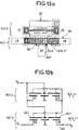
- FIG. 12a symbolically represents a field effect transistor as is commonly done. Derived from this symbolic representation, we have represented in FIG. 12b, a field effect transistor according to the invention having secondary gates GS1 and GS2. This symbolic representation will be used in the description which follows. We will describe in what follows a device for recharging floating grids.
- FIGS. 13a and 13b represent a field effect transistor FET1 as described above with which an element FET2 is combined which can also be a field effect transistor of the same type as FET1.
- transistor FET2 The structure of transistor FET2 is as described above.
- the transistor FET2 has secondary gates which are extensions of the secondary gates GS1 and GS2 of the transistor FET1.
- the main gate of the transistor FET2 is also an extension of the main gate GP of the transistor FET1.
- the source and drain contacts of the transistor FET2 are designated respectively CC and CD.
- the drain contact CD is coupled to the secondary grids GS1 and GS2.
- the transistor FET2 When the potential V GP is made zero the transistor FET2 is blocked. However, in the transistor FET2, the ratio of the section W2 of the channel to its length L2 is much less than 1 while, in the transistor FET1, the ratio of the section W1 of the channel at its length L1 is clearly greater than 1. When the transistor FET2 is blocked the leakage current by FET2 is, more certainly, negligible (because W2 / L2 ⁇ 1) and the secondary gates do not may discharge.
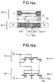
- Figures 14a and 14b show an alternative embodiment of the device of Figures 13a and 13b in which the FET2 transistor of Figures 13 and 13b is replaced by a field effect transistor of known type.
- the transistor FET2 is clearly separated from the field effect structure FET1.
- the ion implantation for the realization of the drains and the sources of the transistors is self-aligned with the secondary gates GS1 and GS2 in the transistor FET1 but cannot be self-ignited with the main gate GP of the transistor FET2 (the main gate GP being performed after ion implantation). This problem does not exist in the device of FIGS. 13a and 13b.
- the source (CC) and the gate of the FET2 transistor are connected to the main gate of the FET1 but according to a variant not shown, they could be connected to the drain (CB) of the FET1. Any other arrangement could also be considered.
- FIG. 15a represents an alternative embodiment of the device of the invention in which no main grid is provided.
- this device comprises a source S, a drain D connected by a channel.
- a floating grid GF Above the canal is a floating grid GF.
- the grid GF is loaded as described above by reverse polarization of the drain-channel and / or source-channel junctions. A zone or accumulation is therefore induced under the grid GF making the device pass. So we made a permanent switch.
- This device can find an application in particular in the control of a matrix device for which there are control conductors (row and column conductors).
- the device of the invention is then placed in series on a row or column conductor and allows the continuity of this conductor to be established on command.
- FIG. 15b represents a variant of the device of FIG. 15a in which there is a device to be controlled D1 such as that of FIG. 15a.
- the device D1 is associated with a charging device D2.
- the device D2 also has a floating gate which is connected to that of the device D1. According to a preferred embodiment of the invention, these two floating grids form a single piece.
Landscapes
- Thin Film Transistor (AREA)
Applications Claiming Priority (2)
| Application Number | Priority Date | Filing Date | Title |
|---|---|---|---|
| FR9205922A FR2691289A1 (fr) | 1992-05-15 | 1992-05-15 | Dispositif semiconducteur à effet de champ, procédé de réalisation et application à un dispositif à commande matricielle. |
| FR9205922 | 1992-05-15 |
Publications (1)
| Publication Number | Publication Date |
|---|---|
| EP0570257A1 true EP0570257A1 (de) | 1993-11-18 |
Family
ID=9429820
Family Applications (1)
| Application Number | Title | Priority Date | Filing Date |
|---|---|---|---|
| EP19930401148 Withdrawn EP0570257A1 (de) | 1992-05-15 | 1993-05-04 | Feldeffekt-Halbleiteranordnung mit sekundärem Gate, Verfahren zur Herstellung und Verwendung in einer Matrix-Ansteuerungsanordnung |
Country Status (3)
| Country | Link |
|---|---|
| EP (1) | EP0570257A1 (de) |
| JP (1) | JPH06283716A (de) |
| FR (1) | FR2691289A1 (de) |
Cited By (6)
| Publication number | Priority date | Publication date | Assignee | Title |
|---|---|---|---|---|
| WO1996022616A1 (en) * | 1995-01-19 | 1996-07-25 | Litton Systems (Canada) Limited | Flat panel imaging device |
| WO2001073854A3 (en) * | 2000-03-25 | 2002-02-28 | Peregrine Semiconductor Corp | Variable capacitor with programmability |
| US6690056B1 (en) | 1999-04-06 | 2004-02-10 | Peregrine Semiconductor Corporation | EEPROM cell on SOI |
| EP1712893A1 (de) * | 2005-04-14 | 2006-10-18 | Agilent Technologies, Inc., A Delaware Corporation | Flacher Sensor mit resonantem Tunneleffekt und dessen Herstellungs- und Anwendungsverfahren. |
| CN114864406A (zh) * | 2022-05-13 | 2022-08-05 | 西安电子科技大学 | 一种双副栅结构的mos抗辐照器件及其制备方法 |
| GB2613939B (en) * | 2021-11-19 | 2024-10-30 | Lg Display Co Ltd | Thin film transistor, thin film transistor substrate and display device |
Citations (9)
| Publication number | Priority date | Publication date | Assignee | Title |
|---|---|---|---|---|
| EP0040251A1 (de) * | 1979-11-12 | 1981-11-25 | Fujitsu Limited | Halbleiter-speichervorrichtung |
| EP0045578A2 (de) * | 1980-07-28 | 1982-02-10 | Fujitsu Limited | Halbleiterspeicheranordnung |
| EP0053075A2 (de) * | 1980-11-26 | 1982-06-02 | Fujitsu Limited | Nichtflüchtiger Speicher |
| EP0166261A2 (de) * | 1984-06-27 | 1986-01-02 | Energy Conversion Devices, Inc. | Statisches Feld induzierte Halbleiteranordnungen |
| EP0333405A2 (de) * | 1988-03-16 | 1989-09-20 | Fujitsu Limited | Speisespannungspotentialanstiegsdetektorschaltung |
| EP0389721A2 (de) * | 1989-03-27 | 1990-10-03 | Ict International Cmos Technology, Inc. | Flash-EPROM-Zelle und Verfahren zu ihrer Herstellung |
| US4994869A (en) * | 1989-06-30 | 1991-02-19 | Texas Instruments Incorporated | NMOS transistor having inversion layer source/drain contacts |
| EP0444712A1 (de) * | 1990-03-02 | 1991-09-04 | Nippon Telegraph And Telephone Corporation | Mehrfachgatter-Dünnfilmtransistor |
| US5063171A (en) * | 1990-04-06 | 1991-11-05 | Texas Instruments Incorporated | Method of making a diffusionless virtual drain and source conductor/oxide semiconductor field effect transistor |
-
1992
- 1992-05-15 FR FR9205922A patent/FR2691289A1/fr not_active Withdrawn
-
1993
- 1993-05-04 EP EP19930401148 patent/EP0570257A1/de not_active Withdrawn
- 1993-05-14 JP JP5136427A patent/JPH06283716A/ja active Pending
Patent Citations (9)
| Publication number | Priority date | Publication date | Assignee | Title |
|---|---|---|---|---|
| EP0040251A1 (de) * | 1979-11-12 | 1981-11-25 | Fujitsu Limited | Halbleiter-speichervorrichtung |
| EP0045578A2 (de) * | 1980-07-28 | 1982-02-10 | Fujitsu Limited | Halbleiterspeicheranordnung |
| EP0053075A2 (de) * | 1980-11-26 | 1982-06-02 | Fujitsu Limited | Nichtflüchtiger Speicher |
| EP0166261A2 (de) * | 1984-06-27 | 1986-01-02 | Energy Conversion Devices, Inc. | Statisches Feld induzierte Halbleiteranordnungen |
| EP0333405A2 (de) * | 1988-03-16 | 1989-09-20 | Fujitsu Limited | Speisespannungspotentialanstiegsdetektorschaltung |
| EP0389721A2 (de) * | 1989-03-27 | 1990-10-03 | Ict International Cmos Technology, Inc. | Flash-EPROM-Zelle und Verfahren zu ihrer Herstellung |
| US4994869A (en) * | 1989-06-30 | 1991-02-19 | Texas Instruments Incorporated | NMOS transistor having inversion layer source/drain contacts |
| EP0444712A1 (de) * | 1990-03-02 | 1991-09-04 | Nippon Telegraph And Telephone Corporation | Mehrfachgatter-Dünnfilmtransistor |
| US5063171A (en) * | 1990-04-06 | 1991-11-05 | Texas Instruments Incorporated | Method of making a diffusionless virtual drain and source conductor/oxide semiconductor field effect transistor |
Non-Patent Citations (1)
| Title |
|---|
| JAPANESE JOURNAL OF APPLIED PHYSICS PART 1 vol. 30, no. 11B, Novembre 1991, TOKYO JP pages 3302 - 3307 KEIJI TANAKA ET AL 'Field-Induction-Drain Thin-Film Transistors for Liquid-Cristal Display Applications' * |
Cited By (9)
| Publication number | Priority date | Publication date | Assignee | Title |
|---|---|---|---|---|
| WO1996022616A1 (en) * | 1995-01-19 | 1996-07-25 | Litton Systems (Canada) Limited | Flat panel imaging device |
| US5917210A (en) * | 1995-01-19 | 1999-06-29 | Litton Systems Canada Limited | Flat panel imaging device |
| US6667506B1 (en) | 1999-04-06 | 2003-12-23 | Peregrine Semiconductor Corporation | Variable capacitor with programmability |
| US6690056B1 (en) | 1999-04-06 | 2004-02-10 | Peregrine Semiconductor Corporation | EEPROM cell on SOI |
| WO2001073854A3 (en) * | 2000-03-25 | 2002-02-28 | Peregrine Semiconductor Corp | Variable capacitor with programmability |
| EP1712893A1 (de) * | 2005-04-14 | 2006-10-18 | Agilent Technologies, Inc., A Delaware Corporation | Flacher Sensor mit resonantem Tunneleffekt und dessen Herstellungs- und Anwendungsverfahren. |
| GB2613939B (en) * | 2021-11-19 | 2024-10-30 | Lg Display Co Ltd | Thin film transistor, thin film transistor substrate and display device |
| US12495678B2 (en) | 2021-11-19 | 2025-12-09 | Lg Display Co., Ltd. | Thin film transistor, thin film transistor substrate and display apparatus |
| CN114864406A (zh) * | 2022-05-13 | 2022-08-05 | 西安电子科技大学 | 一种双副栅结构的mos抗辐照器件及其制备方法 |
Also Published As
| Publication number | Publication date |
|---|---|
| JPH06283716A (ja) | 1994-10-07 |
| FR2691289A1 (fr) | 1993-11-19 |
Similar Documents
| Publication | Publication Date | Title |
|---|---|---|
| EP0350351B1 (de) | Fotodiode und Fotodiodenmatrix aus II-VI-Halbleitermaterial und Herstellungsverfahren dafür | |
| FR2676864A1 (fr) | Procede de fabrication de transistor mos a recouvrement grille-drain et structure correspondante. | |
| FR2795554A1 (fr) | Procede de gravure laterale par trous pour fabriquer des dis positifs semi-conducteurs | |
| EP2680311A1 (de) | Tunneleffekttransistor | |
| EP1483793B1 (de) | Leistungs-schottkydiode mit sicoi-substrat und diesbezügliches herstellungsverfahren | |
| EP0797252B1 (de) | Silizium auf Isolator-Substrat zum Herstellen von Transistoren und Verfahren zum Vorbereiten eines derartigen Substrats | |
| EP0432044A1 (de) | III-V-Verbindungsleistungstransistor auf Siliciumsubstrat und Verfahren zur Herstellung | |
| EP0046422B1 (de) | Nichtflüchtiger GaAs-Speicherfeldeffekttransistor | |
| EP0624943B1 (de) | Seriengeschaltetes Strombegrenzerbauelement | |
| FR2496342A1 (fr) | Dispositif semi-conducteur du type metal-oxyde-semi-conducteur et son procede de fabrication | |
| FR2708142A1 (fr) | Procédé de fabrication d'un transistor en technologie silicium sur isolant. | |
| EP0570257A1 (de) | Feldeffekt-Halbleiteranordnung mit sekundärem Gate, Verfahren zur Herstellung und Verwendung in einer Matrix-Ansteuerungsanordnung | |
| EP0503731B1 (de) | Verfahren zur Realisierung eines Transistors mit hoher Elektronenbeweglichkeit | |
| FR2496990A1 (fr) | Transistor a effet de champ a barriere schottky | |
| EP3826061B1 (de) | Hybride elektronische vorrichtung und verfahren zur herstellung einer solchen vorrichtung | |
| EP0058577B1 (de) | Halbleiteranordnung mit Elektronenablenkung vom Typ des "ballistischen Transportes" und Verfahren zum Herstellen einer solchen Anordnung | |
| EP0508843B1 (de) | Josephsoneffekt-Halbleiteranordnung | |
| FR2791178A1 (fr) | NOUVEAU DISPOSITIF SEMI-CONDUCTEUR COMBINANT LES AVANTAGES DES ARCHITECTURES MASSIVE ET soi, ET PROCEDE DE FABRICATION | |
| EP1350267A1 (de) | Integrierter schaltkreis und herstellungsverfahren | |
| EP4088312B1 (de) | Verfahren zur herstellung einer halbleiter-auf-isolator-struktur für hochfrequenzanwendungen | |
| EP3903342B1 (de) | Halbleiterstruktur für digitale und hochfrequente anwendungen und verfahren zur herstellung einer solchen struktur | |
| EP4078116B1 (de) | Hochempfindliches bauteil zur detektion elektromagnetischer strahlung und verfahren zur herstellung eines solchen bauteils | |
| FR2752338A1 (fr) | Transistor en couche mince a siliciure | |
| FR3136109A1 (fr) | Dispositif semiconducteur du type silicium sur isolant et procédé de fabrication correspondant | |
| EP0434502B1 (de) | Hybrider Photosensor |
Legal Events
| Date | Code | Title | Description |
|---|---|---|---|
| PUAI | Public reference made under article 153(3) epc to a published international application that has entered the european phase |
Free format text: ORIGINAL CODE: 0009012 |
|
| AK | Designated contracting states |
Kind code of ref document: A1 Designated state(s): DE GB IT NL |
|
| RAP3 | Party data changed (applicant data changed or rights of an application transferred) |
Owner name: THOMSON-CSF |
|
| 17P | Request for examination filed |
Effective date: 19940228 |
|
| 17Q | First examination report despatched |
Effective date: 19960927 |
|
| STAA | Information on the status of an ep patent application or granted ep patent |
Free format text: STATUS: THE APPLICATION IS DEEMED TO BE WITHDRAWN |
|
| 18D | Application deemed to be withdrawn |
Effective date: 19980324 |