EP0166261A2 - Statisches Feld induzierte Halbleiteranordnungen - Google Patents
Statisches Feld induzierte Halbleiteranordnungen Download PDFInfo
- Publication number
- EP0166261A2 EP0166261A2 EP85106685A EP85106685A EP0166261A2 EP 0166261 A2 EP0166261 A2 EP 0166261A2 EP 85106685 A EP85106685 A EP 85106685A EP 85106685 A EP85106685 A EP 85106685A EP 0166261 A2 EP0166261 A2 EP 0166261A2
- Authority
- EP
- European Patent Office
- Prior art keywords
- layer
- field effect
- channel
- further characterized
- transistor
- Prior art date
- Legal status (The legal status is an assumption and is not a legal conclusion. Google has not performed a legal analysis and makes no representation as to the accuracy of the status listed.)
- Withdrawn
Links
Images



Classifications
-
- H—ELECTRICITY
- H10—SEMICONDUCTOR DEVICES; ELECTRIC SOLID-STATE DEVICES NOT OTHERWISE PROVIDED FOR
- H10D—INORGANIC ELECTRIC SEMICONDUCTOR DEVICES
- H10D8/00—Diodes
-
- H—ELECTRICITY
- H10—SEMICONDUCTOR DEVICES; ELECTRIC SOLID-STATE DEVICES NOT OTHERWISE PROVIDED FOR
- H10D—INORGANIC ELECTRIC SEMICONDUCTOR DEVICES
- H10D12/00—Bipolar devices controlled by the field effect, e.g. insulated-gate bipolar transistors [IGBT]
- H10D12/211—Gated diodes
-
- H—ELECTRICITY
- H10—SEMICONDUCTOR DEVICES; ELECTRIC SOLID-STATE DEVICES NOT OTHERWISE PROVIDED FOR
- H10D—INORGANIC ELECTRIC SEMICONDUCTOR DEVICES
- H10D30/00—Field-effect transistors [FET]
- H10D30/40—FETs having zero-dimensional [0D], one-dimensional [1D] or two-dimensional [2D] charge carrier gas channels
- H10D30/47—FETs having zero-dimensional [0D], one-dimensional [1D] or two-dimensional [2D] charge carrier gas channels having two-dimensional [2D] charge carrier gas channels, e.g. nanoribbon FETs or high electron mobility transistors [HEMT]
-
- H—ELECTRICITY
- H10—SEMICONDUCTOR DEVICES; ELECTRIC SOLID-STATE DEVICES NOT OTHERWISE PROVIDED FOR
- H10D—INORGANIC ELECTRIC SEMICONDUCTOR DEVICES
- H10D30/00—Field-effect transistors [FET]
- H10D30/40—FETs having zero-dimensional [0D], one-dimensional [1D] or two-dimensional [2D] charge carrier gas channels
- H10D30/47—FETs having zero-dimensional [0D], one-dimensional [1D] or two-dimensional [2D] charge carrier gas channels having two-dimensional [2D] charge carrier gas channels, e.g. nanoribbon FETs or high electron mobility transistors [HEMT]
- H10D30/471—High electron mobility transistors [HEMT] or high hole mobility transistors [HHMT]
- H10D30/475—High electron mobility transistors [HEMT] or high hole mobility transistors [HHMT] having wider bandgap layer formed on top of lower bandgap active layer, e.g. undoped barrier HEMTs such as i-AlGaN/GaN HEMTs
- H10D30/4755—High electron mobility transistors [HEMT] or high hole mobility transistors [HHMT] having wider bandgap layer formed on top of lower bandgap active layer, e.g. undoped barrier HEMTs such as i-AlGaN/GaN HEMTs having wide bandgap charge-carrier supplying layers, e.g. modulation doped HEMTs such as n-AlGaAs/GaAs HEMTs
-
- H—ELECTRICITY
- H10—SEMICONDUCTOR DEVICES; ELECTRIC SOLID-STATE DEVICES NOT OTHERWISE PROVIDED FOR
- H10D—INORGANIC ELECTRIC SEMICONDUCTOR DEVICES
- H10D30/00—Field-effect transistors [FET]
- H10D30/60—Insulated-gate field-effect transistors [IGFET]
- H10D30/67—Thin-film transistors [TFT]
- H10D30/6728—Vertical TFTs
-
- H—ELECTRICITY
- H10—SEMICONDUCTOR DEVICES; ELECTRIC SOLID-STATE DEVICES NOT OTHERWISE PROVIDED FOR
- H10D—INORGANIC ELECTRIC SEMICONDUCTOR DEVICES
- H10D30/00—Field-effect transistors [FET]
- H10D30/60—Insulated-gate field-effect transistors [IGFET]
- H10D30/67—Thin-film transistors [TFT]
- H10D30/6729—Thin-film transistors [TFT] characterised by the electrodes
- H10D30/673—Thin-film transistors [TFT] characterised by the electrodes characterised by the shapes, relative sizes or dispositions of the gate electrodes
- H10D30/6731—Top-gate only TFTs
-
- H—ELECTRICITY
- H10—SEMICONDUCTOR DEVICES; ELECTRIC SOLID-STATE DEVICES NOT OTHERWISE PROVIDED FOR
- H10D—INORGANIC ELECTRIC SEMICONDUCTOR DEVICES
- H10D30/00—Field-effect transistors [FET]
- H10D30/60—Insulated-gate field-effect transistors [IGFET]
- H10D30/67—Thin-film transistors [TFT]
- H10D30/6729—Thin-film transistors [TFT] characterised by the electrodes
- H10D30/673—Thin-film transistors [TFT] characterised by the electrodes characterised by the shapes, relative sizes or dispositions of the gate electrodes
- H10D30/6733—Multi-gate TFTs
-
- H—ELECTRICITY
- H10—SEMICONDUCTOR DEVICES; ELECTRIC SOLID-STATE DEVICES NOT OTHERWISE PROVIDED FOR
- H10D—INORGANIC ELECTRIC SEMICONDUCTOR DEVICES
- H10D30/00—Field-effect transistors [FET]
- H10D30/60—Insulated-gate field-effect transistors [IGFET]
- H10D30/67—Thin-film transistors [TFT]
- H10D30/6729—Thin-film transistors [TFT] characterised by the electrodes
- H10D30/673—Thin-film transistors [TFT] characterised by the electrodes characterised by the shapes, relative sizes or dispositions of the gate electrodes
- H10D30/6733—Multi-gate TFTs
- H10D30/6734—Multi-gate TFTs having gate electrodes arranged on both top and bottom sides of the channel, e.g. dual-gate TFTs
-
- H—ELECTRICITY
- H10—SEMICONDUCTOR DEVICES; ELECTRIC SOLID-STATE DEVICES NOT OTHERWISE PROVIDED FOR
- H10D—INORGANIC ELECTRIC SEMICONDUCTOR DEVICES
- H10D30/00—Field-effect transistors [FET]
- H10D30/60—Insulated-gate field-effect transistors [IGFET]
- H10D30/67—Thin-film transistors [TFT]
- H10D30/674—Thin-film transistors [TFT] characterised by the active materials
- H10D30/6741—Group IV materials, e.g. germanium or silicon carbide
-
- H—ELECTRICITY
- H10—SEMICONDUCTOR DEVICES; ELECTRIC SOLID-STATE DEVICES NOT OTHERWISE PROVIDED FOR
- H10D—INORGANIC ELECTRIC SEMICONDUCTOR DEVICES
- H10D30/00—Field-effect transistors [FET]
- H10D30/60—Insulated-gate field-effect transistors [IGFET]
- H10D30/67—Thin-film transistors [TFT]
- H10D30/674—Thin-film transistors [TFT] characterised by the active materials
- H10D30/6741—Group IV materials, e.g. germanium or silicon carbide
- H10D30/6743—Silicon
-
- H—ELECTRICITY
- H10—SEMICONDUCTOR DEVICES; ELECTRIC SOLID-STATE DEVICES NOT OTHERWISE PROVIDED FOR
- H10D—INORGANIC ELECTRIC SEMICONDUCTOR DEVICES
- H10D30/00—Field-effect transistors [FET]
- H10D30/60—Insulated-gate field-effect transistors [IGFET]
- H10D30/67—Thin-film transistors [TFT]
- H10D30/674—Thin-film transistors [TFT] characterised by the active materials
- H10D30/6741—Group IV materials, e.g. germanium or silicon carbide
- H10D30/6743—Silicon
- H10D30/6746—Amorphous silicon
-
- H—ELECTRICITY
- H10—SEMICONDUCTOR DEVICES; ELECTRIC SOLID-STATE DEVICES NOT OTHERWISE PROVIDED FOR
- H10D—INORGANIC ELECTRIC SEMICONDUCTOR DEVICES
- H10D62/00—Semiconductor bodies, or regions thereof, of devices having potential barriers
- H10D62/40—Crystalline structures
- H10D62/402—Amorphous materials
-
- H—ELECTRICITY
- H10—SEMICONDUCTOR DEVICES; ELECTRIC SOLID-STATE DEVICES NOT OTHERWISE PROVIDED FOR
- H10D—INORGANIC ELECTRIC SEMICONDUCTOR DEVICES
- H10D62/00—Semiconductor bodies, or regions thereof, of devices having potential barriers
- H10D62/80—Semiconductor bodies, or regions thereof, of devices having potential barriers characterised by the materials
- H10D62/82—Heterojunctions
-
- H—ELECTRICITY
- H10—SEMICONDUCTOR DEVICES; ELECTRIC SOLID-STATE DEVICES NOT OTHERWISE PROVIDED FOR
- H10D—INORGANIC ELECTRIC SEMICONDUCTOR DEVICES
- H10D64/00—Electrodes of devices having potential barriers
- H10D64/60—Electrodes characterised by their materials
- H10D64/602—Heterojunction gate electrodes for FETs
-
- H—ELECTRICITY
- H10—SEMICONDUCTOR DEVICES; ELECTRIC SOLID-STATE DEVICES NOT OTHERWISE PROVIDED FOR
- H10D—INORGANIC ELECTRIC SEMICONDUCTOR DEVICES
- H10D64/00—Electrodes of devices having potential barriers
- H10D64/60—Electrodes characterised by their materials
- H10D64/66—Electrodes having a conductor capacitively coupled to a semiconductor by an insulator, e.g. MIS electrodes
- H10D64/68—Electrodes having a conductor capacitively coupled to a semiconductor by an insulator, e.g. MIS electrodes characterised by the insulator, e.g. by the gate insulator
-
- H—ELECTRICITY
- H10—SEMICONDUCTOR DEVICES; ELECTRIC SOLID-STATE DEVICES NOT OTHERWISE PROVIDED FOR
- H10D—INORGANIC ELECTRIC SEMICONDUCTOR DEVICES
- H10D84/00—Integrated devices formed in or on semiconductor substrates that comprise only semiconducting layers, e.g. on Si wafers or on GaAs-on-Si wafers
- H10D84/80—Integrated devices formed in or on semiconductor substrates that comprise only semiconducting layers, e.g. on Si wafers or on GaAs-on-Si wafers characterised by the integration of at least one component covered by groups H10D12/00 or H10D30/00, e.g. integration of IGFETs
- H10D84/82—Integrated devices formed in or on semiconductor substrates that comprise only semiconducting layers, e.g. on Si wafers or on GaAs-on-Si wafers characterised by the integration of at least one component covered by groups H10D12/00 or H10D30/00, e.g. integration of IGFETs of only field-effect components
- H10D84/83—Integrated devices formed in or on semiconductor substrates that comprise only semiconducting layers, e.g. on Si wafers or on GaAs-on-Si wafers characterised by the integration of at least one component covered by groups H10D12/00 or H10D30/00, e.g. integration of IGFETs of only field-effect components of only insulated-gate FETs [IGFET]
- H10D84/85—Complementary IGFETs, e.g. CMOS
-
- H—ELECTRICITY
- H10—SEMICONDUCTOR DEVICES; ELECTRIC SOLID-STATE DEVICES NOT OTHERWISE PROVIDED FOR
- H10D—INORGANIC ELECTRIC SEMICONDUCTOR DEVICES
- H10D88/00—Three-dimensional [3D] integrated devices
Definitions
- This invention relates generally to improved semiconductor devices, and more particularly to such devices made of amorphous semiconductor materials.
- Proximity doping which may also be termed “modulation doping” or “transfer doping” is a process whereby the electronic properties of a semiconductor layer are modified by the induction of an electric field therein and the bending of energy bands due to the proximity of said semiconductor layer to specifically designed superadjacent and/or subjacent layers.
- proximity doping can be achieved by placing a body of intrinsic semiconductor material in close proximity to a field inducing layer which has a net electric charge.
- the electric field induced in the intrinsic semiconductor material acts upon that material to shift its Fermi level relative to the energy levels of its conduction and valence bands without the introduction of dopant atoms into the semiconductor material.
- This field induced shift of the Fermi level has the effect of changing the number of electrons and holes in the semiconductor material, as would the introduction of atomic donor or acceptor impurities into that material, but it does not have the adverse effect, of introducing defect states as would the introduction of such impurities.
- a channel region of amorphous material is placed in electrical series between a source and a drain electrode.
- a gate electrode is electrically insulated from the channel region. The gate is positioned so that when a certain threshold voltage is supplied to it, the resultant electrostatic potential in the channel region induces enough charge carriers into that region to make it conductive.
- the threshold voltage required to switch a channel region of substantially intrinsic amorphous semiconductor material from a substantially non-conducting state to a substantially conducting state is higher than desirable for many applications.
- defect states decrease the change in conductivity which results from a given change in induced voltage, decreasing the amplification and sensitivity of field effect transistors which use such impurity doped amorphous materials.
- a field effect transistor of the type which includes a source, a drain, and a channel region of amorphous semiconductor material in which a conduction channel can be formed between the source and the drain.
- the transistor further includes a gate adapted, in response to an applied voltage, to induce a change in the conductivity of the channel region.
- the invention provides the improvement of a field inducing body of material, formed with a built-in charge, in field effect proximity to the channel region, so as to shift the Fermi level of the channel region by means of field effect rather than by atomic impurity doping.
- the field inducing body can have either a positive or a negative built in charge, shifting the Fermi level to make the channel region either more n-type or more p-type.
- the field inducing body can be used to shift the Fermi level of the channel region either to reduce the gate voltage required to turn the transistor on, or to make the transistor substantially on without the application of any gate voltage, so that a gate voltage must actually be applied to turn the channel region off.
- both the field inducing body and the amorphous semiconductor material in which the channel region is located are formed of layers of deposited material which are in contact with each other, and the built-in charge of the field inducing layer is formed in the creation of those layers.
- the field inducing layer is made of an amorphous hydrogenated silicon carbide alloy, an electrical insulator, which, when formed in contact with the amorphous semiconductor material in which the channel region is located, attracts a negative built-in charge, tending to shift the Fermi level in the channel region to make that material more p-type.
- the field inducing layer is made of an amorphous hydrogenated silicon nitride alloy, also an electrical insulator, which, when formed in contact with the amorphous semiconductor material in which its channel region is located, attains a positive built-in charge, tending to shift the Fermi level in the channel region to make that material more n-type.
- the field inducing layer has atomic impurity dopants such as phosphorous or boron added to it to cause the charged layer to obtain an additional component of built-in charge by charge transfers with adjacent amorphous semiconductor material.
- an electronic circuit of the type having two field effect transistors in which the gate of both transistors are responsive to a common input. Both transistors have either their source or drain connected to form a common output, and one transistors has either its source or drain connected to a relatively positive power supply, while the other transistor has either its source or drain connected to a relatively negative power supply.
- the channel regions of the two transistors are selected so that a voltage supplied to the common input which turns one transistor on, will turn the other off.
- One aspect of the present invention is the inclusion in at least one of the two transistors of a field inducing body of material, formed with a built-in charge, in field effect proximity to the channel region of that transistor so as to shift the Fermi level of that channel region by means of a field effect rather than by atomic impurity doping.
- the two transistors are both metal oxide semiconductor transistors, and one of them is an n-channel transistor and the other is a p-channel transistor, so the two transistors form a CMOS circuit.
- each transistor would have a field inducing body, or layer, of material formed with a built-in charge in field effect proximity to its channel regions so as to shift the Fermi level thereof by means of field effect rather than atomic impurity doping.
- a semiconductor device which comprises a first region of material consisting essentially of an amorphous semiconductor material.
- the device further includes a first field inducing body of material, formed with a built-in charge, in field effect proximity to the first region, so as to proximity dope the first region by shifting the Fermi level thereof toward one band edge, either the conduction or valance band edge, by means of a field effect rather than by atomic impurity doping.
- the device also includes a second region of material which has its Fermi level positioned relatively further away from the band edge toward which the Fermi level of the first region has been shifted. The first and second regions are in contact with each other so as to form a junction.
- the second region of material consists essentially of an amorphous semiconductor material and has a second field inducing body, located in field effect proximity to the second region, formed with a built in charge of a polarity opposite that of the first field inducing body.
- the built-in charge of the second field inducing body proximity dopes the second region by shifting the Fermi level thereof toward the band edge opposite that toward which the Fermi level of the first region is shifted.
- the junction between the first and second regions forms a p-n junction.
- a variably chargeable body of material is located in field effect proximity to the first region.
- the variably chargeable body variably alters, by means of a field effect, the amount which the Fermi level in the first region is shifted toward a given band edge in the vacinity of the junction.
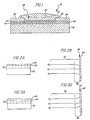
- a thin film field effect transistor 10 is shown which embodies the present invention.
- the transistor 10 is formed on a substrate 12, which can be formed, for example, from glass.
- a thin field inducing layer 16 Overlying substrate 12 is a thin field inducing layer 16.
- Overlying layer 16 is a layer 18 of deposited amorphous semiconductor material.
- amorphous is meant an alloy or material which has long-range disorder, although it may have short or intermediate range order or even contain microcrystalline phases or some crystalline inclusions. Such material can include, for example, microcrystalline semiconductor materials.
- Layer 18 can, for example, be formed of an amorphous alloy of silicon, germanium, or silicon and germanium.
- the amorphous semiconductor material of layer 18 is made of a substantially intrinsic amorphous semiconductor material, that is, of an amorphous semiconductor material without any significant concentration of impurity doping atoms.
- a substantially intrinsic amorphous semiconductor material that is, of an amorphous semiconductor material without any significant concentration of impurity doping atoms.
- some intrinsic, or undoped, amorphous semiconductor materials have a Fermi level which is slightly closer to the conduction band than the valence band, thereby giving them a slight preponderance of n-type charge carriers over p-type carriers.
- the field-inducing body, or layer, 16 is in contact with the amorphous semiconductor layer 18 and is made of a material, which is formed with a built-in charge.
- the field inducing layer can be formed of an amorphous hydrogenated silicon carbide alloy having the general formula amorphous Si:C:H.
- Such a layer can be deposited from a glow discharge decomposition of a gaseous mixture of silane, methane and hydrogen.
- the field inducing layer can be made of an amorphous hydrogenated silicon nitride alloy having the general formula amorphous Si:N:H.
- Such an alloy can be deposited from a glow discharge decomposition of a gaseous mixture of silane, amonia and hydrogen.
- Layers 16 and 18 can be deposited on substrate 12 using the method and apparatus described in U.S. Patent Application Serial No.
- An important aspect of the present invention is the use of a negatively charged layer, such as Si:C:H, as the material of a field inducing layer for proximity doping in a semiconductor device.
- a negatively charged layer such as Si:C:H
- Intrinsic amorphous semiconductor materials such as Si:H and Si:F:H tend to have more defect states in the bottom half of the energy gap between the conduction and valence band edges than in the top half of that energy gap. As a result it is more difficult to shift the Fermi level downwards to make such materials p-type than it is to shift it upward to make them n-type.
- a source 22 and a drain 24 Disposed over layer 18 are a source 22 and a drain 24, which are both made of metal in the embodiment shown. Care should be taken that both source 22 and drain 24 form an ohmic contact with the amorphous semiconductor material of layer 18. Since the substantially intrinsic material of layer 18 has a slight n-type characteristic, it is best that the source and drain electrodes be made of low work function metals, such as magnesium, chromium or aluminum. For an even better ohmic contact a layer of n+ amorphous semiconductor material should be placed between such low work function metals and layer 18, in a manner similar to that shown in Figure 5, discussed below.
- Source 22 and drain 24 are separated by a gap 25.
- a channel region 20 is located in the portions of layer 18 which extends across the gap 25 between the source 22 and the drain 24.
- a conducting channel can be formed in this channel region during the operation of the field effect transistor 10. Because the channel region 20 is located in layer 18, that layer can be referred to as the channel layer.
- a second field inducing layer 26 is disposed over the gap 25, so as to be in field effect proximity with the channel region 20.
- the field inducing layer 26 can be made of the same material as the field inducing layer 16, and it cooperates with the layer 16 to shift the Fermi level of the amorphous semiconductor material in the channel region 20.
- the field inducing layers 16 and 26 are made of materials which are insulators. Amorphous alloys of silicon carbide and silicon nitride can both be considered insulators, since they have a conductivity lower than that of intrinsic amorphous silicon:hydrogen alloys. It is important that field inducing layer 26, which is connected to both source 22 and drain 24 not be a conductor, otherwise it would electrically short the channel region 20.
- gate insulator 28 Overlying the field inducing layer 26 is a layer of gate insulator 28, which can be formed, for example, from a silicon oxide (SiO x ). Then over the gate insulator 28 a gate 30 is formed of a metal such as aluminum.
- the thin film transistor 10 operates in a manner similar to that of traditional thin film amorphous semiconductor field effect transistors.
- a voltage is placed across the source 22 and the drain 24, but the conductivity of the amorphous semiconductor material in the channel layer 18, is sufficiently low that substantially no current will flow between the source and drain in the absence of a voltage applied to gate 30.
- the field generated by the charge on gate 30 shifts the Fermi level in the channel region 20, attracting to the channel region charge carriers of a polarity opposite that of the voltage on gate 30.
- the charge carriers induced into the channel region 20 greatly increase its conductivity, thereby increasing the current flow between the source 22 and the drain 24.
- a novel aspect of the present invention is the use of field inducing layers, such as layer 26 and 16, to shift the Fermi level of the channel region in a field effect thin film amorphous semiconductor transistor.
- Figures 2A, 2B, 3A and 3B show the effect of such field inducing layers upon the Fermi level of an adjacent amorphous semiconductor material.
- Figure 2A shows a proximity structure comprised of a layer 32 of substantially intrinsic amorphous silicon alloy, such as Si:F:H or Si:H similar to layer 18 of Figure 1, placed in contact with a charged field inducing layer 34, similiar to layer 26 of Figure 1. Between layers 32 and 34 is a junction 36 at which the two layers meet. Since layer 34 has a positive charge, it induces a field into the layer 32, which increases the concentration of negative charge carriers, or free electrons, in a portion 38 of layer 32 adjacent layer 34.
- Figure 2B shows how the energy level E C of the conduction band edge and the energy level E v of the valence band edge of the intrinsic layer 32 are shifted relative to the Fermi level E F of that layer by the positive charge on layer 34.
- the relative position of the Fermi level E F between the conduction band edge E C and the valence band edge E v varies as a function of the relative number of free electrons to holes.
- the excess of free electrons attracted by the positively charged layer 34 into region 38 shifts the Fermi level E F in that region closer to E C and further from E V .
- Figures 3A and 3B are identical to Figures 2A and 2B except that the charged field inducing layer 42 in Figures 3A and 3B has a negative, rather than a positive charge, which induces a positive charge, or an excess of holes, in the region 46 of the intrinsic layer 32 near the junction 44 with the field inducing layer 42.
- the Fermi level E F in that region is shifted closer to the valence band edge E V , and further from the conduction band edge E C . Since the Fermi level E F is flat at equilibrium, the shift in the Fermi level relative to E c and E v results in a bending of E C and E V , as shown in Figure 3B.
- region 46 the characteristics of a p-type semiconductor. This proximity doping is achieved without the high number of defect states which would be required to obtain a similar number of excess holes by means of atomic impurity doping.
- the charge on the field inducing layers 34 and 42 is called a built-in charge because it is a charge built-in to those layers at the creation of the device of which they are part. Under intended operating conditions the built-in charge is retained by the field inducing layers during the useful life of the devices of which they are part. It is not yet clearly understood what causes the built-in charge to accumulate on field inducing layers formed of materials such as amorphous alloys of Si:C:H or Si:N:H.
- the built-in charge formed in or on the field inducing layer is caused by charge carriers trapped at the formation of the field inducing layer in deep traps located within the material of that layer or at its interface with the amorphous semiconductor layer.
- Deep traps are usually formed by defects, such as dangling bonds or atomic vacancies, which can trap free electrons or holes. They have energy levels located deep in the middle of the gap between the conduction and valence bands. As a result, a large amount of energy is required to extricate electrons or holes caught with such traps. In fact, depending on the depth of the trap, the average amount of time required for a carrier to escape can vary from microseconds to many years.
- the apparently permanent built-in charge observed on field inducing layers of the type discussed above is actually comprised of charge captured in deep traps which is slowly discharging, but is doing so at a rate too slow to be readily measurable.
- the built-in charge observed on such field inducing layers results from other causes.
- the built-in charge results from the fact that the Fermi level in the material of such field inducing layers is located at an energy level different from that in the adjacent intrinsic amorphous semiconductor. If that is the case, when the two layers are placed in contact during their creation, diffusion would cause electrons to flow between the field inducing layer and the adjacent intrinsic semiconductor layer to equalize the Fermi levels of the two materials. The net result would be that the field inducing layer develops a built-in charge, and the intrinsic semiconductor material attains an opposite charge.
- the field inducing layers used to shift the Fermi level of the channel region are formed of materials known to have a Fermi level different from that of the semiconductor materials of their associated channel regions.
- a semiconductor junction is formed between each such field inducing layer and the semiconductor material in which its associated channel region is located. Electrons flow across this junction so as to equalize the Fermi levels in both its sides, creating a charge on each side of the junction.
- Suitable materials for use in such field inducing layers include doped amorphous semiconductors such as amorphous Si:H or Si:F:H alloys doped with either boron or phosphorus atoms.
- an intrinsic amorphous semiconductor material of a transistor When an intrinsic amorphous semiconductor material of a transistor has its Fermi level shifted by a field inducing layer, the operating characteristics of that transistor are changed.
- a transistor of the type shown in Figure 1 normally ope-rates by having a voltage placed on gate 30 which shifts the Fermi level of its channel region 20 sufficiently close to either the conduction band or the valence band to generate enough electrons or holes, respectively, to make that channel region conductive.
- a field inducing layer such as layers 26 and 16 of Figure 1
- the Fermi level can be shifted closer to either the conduction or valence band in the absence of such an applied voltage, reducing the amount which a gate voltage, when applied, has to shift the Fermi level to turn the transistor on.
- the field inducing layer reduces the threshold voltage which must be applied to gate 30 to turn on transistor 10.
- the Fermi level of channel region 20 can be shifted sufficiently close to either the conduction band or valence band so that the channel region 20 is substantially conducting in the absence of any voltage applied to gate 30.
- the transistor will be normally on, and a voltage will have to be applied to gate 30 to shift the Fermi level back toward the center of the gap between the conduction and valence bands, to turn the transistor off.
- One way to increase the strength of the built-in charge on a field inducing layer is by adding impurity dopants to the materials of such layers.
- materials such as amorphous alloys of silicon nitride and silicon carbide naturally form a built-in charge when layers of such material are formed in contact with amorphous silicon alloys such as Si:F:H and Si:H.
- Such materials may be termed intrinsically charging materials since they form such built-in charge when used in the intrinsic form, that is, when used without the addition of any impurity dopants.
- impurity doping atoms can be added to the intrinsically charging material of a field inducing layer.
- the built-in charge formed has not only a significant component resulting from the properties of the intrinsically charging material, but also an additional significant component resulting from charge transfer with a adjacent layer of amorphous semiconductor material caused by the presence of such impurity doping atoms.
- the impurity doping atoms could include elements such as boron, which tend to form negative ions when placed in semiconductor materials.
- elements such as phosphorus, which tend to form positive ions could be used.
- Another way to increase the shift in the Fermi level of an intrinsic amorphous semiconductor channel region is to place two field inducing layers in close proximity to that channel region, as is shown in Figure 1 by the use of layers 16 and 26.
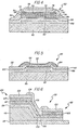
- Transistor 50 has a plurality of channel layers 52 and 54, each having a channel region 55 in which a conductive channel can be formed between a source 56 and a drain 58.
- the thin film transistor 50 is formed by placing a first gate electrode 60 upon a substrate 62 using conventional photolithographic means. Then a layer of gate insulator 64 is placed on top of the gate, again by photolithographic means.
- an alternating series of layers consisting of field inducing layer 66, amorphous semiconductor layer 52, field inducing layer 68, amorphous semiconductor layer 54, and field inducing layer 70, is placed on top of the gate insulator 64 by the method described in the above mentioned U.S. Patent Application Serial No. 558,959. Then this multilayered structure is etched to cut generally opposing verticle sides 72 and 74 against which the metal source and drain contacts 56 and 58 can be disposed by photolithographic techniques.
- the source 56 and drain 58 should be made of a metal which forms an ohmic contacts with the amorphous semiconductor material of layers 52 and 54.
- another layer of gate insulator 76 can be placed over the top of the multilayered structure, and then a metal gate electrode 78 can be placed on top of layer 76.
- the transistor 50 operates in a manner substantially similar to that of transistor 10 shown in Figure 1.
- the field inducing layers 66, 68 and 70 operate to shift the Fermi level of the amorphous semiconductor material contained in layers 52 and 54, and, thus, to alter the amount of gate voltage which has to be applied to gates 60 and 78 to either'turn the transistor on or off.
- One of the major advantages of a transistor such as transistor 50, shown in Figure 4, over transistor 10, shown in Figure 1, is that, because transistor 50 has a plurality of current conduction layers 52 and 54, it is capable of passing more current. If it is desired to make a proximity doped transistor according to the present invention capable of switching even larger amounts of current than that shown in Figure 4, a transistor having more than two vertically arrayed channel layers is formed. In such a transistor each channel layer is formed adjacent to a field inducing layer, and one or more insulated gates are sandwiched between the plurality of channel layers.
- transistor 80 is shown.
- the general configuration of transistor 80 is similar to that of the transistors described in the above mentioned U.S. Patent Application Serial No. 590,836.
- the transistor 80 is formed by placing a gate 82 upon a transparent substrate 84, which can be formed, for example, of glass.
- a relatively transparent gate insulator 86 is placed over the gate and a layer of photoresist, not shown in Figure 4, is placed over the insulator 86.
- Light is transmitted through the substrate 84, so all but the portion of the photoresist directly above the gate 82, is exposed.
- the exposed photoresist is removed, leaving the gate insulator 86 covered by a portion of exposed photoresist immediately above gate 82.
- a layer of metal is placed down over the oxide layer 86 and the unexposed photoresist.
- the unexposed photoresist, and the metal on top of it, are removed by etching, leaving two separated portions of the deposited metal layer, one of which forms the source 88 of the transistor, and the other which forms the drain 90.
- a layer of amorphous semiconductor 92 is placed down over the gap between the source 88 and the drain 90.
- a thin field inducing layer 94 approximately 10 to 100 angstroms thick is placed over the amorphous layer 92.
- a major advantage of transistors such as that shown in Figure 5, is that because there is little overlap between their gate and their source or drain, the capacitance between those electrodes is minimized. This has the beneficial effect of increasing the frequency response of such transistors.
- the field inducing layer 94 is on the opposite side of the layer of amorphous semiconductor material 92 from the gate insulator 86.
- a field inducing layer 100 could be placed on top of the gate insulator 86, either in replacement of, or in addition to, the field inducing layer 94.
- the thin film transistor 110 has a configuration substantially the same as that described in the above mentioned U.S. Patent Application Serial No. 549,979.
- a gate oxide 116 is deposited over the gate 112, and then layer of amorphous semiconductor material 118 is deposited over the gate insulator 116.
- a source 120 and a drain 121 are placed over the amorphous semiconductor material 118, as described in the above mentioned U.S. Patent Application Serial No. 549,979.
- the doped semiconductor 123 provides a good ohmic contact between the metal 122 of source 120 and drain 121 and the layer 118 of amorphous semiconductor material.
- the metal 122 can be, for example, aluminum or chromium, and the doped semiconductor 123 is preferably an n-type amorphous silicon alloy including fluorine.
- the gate insulator layer 116 is placed down before the amorphous semiconductor layer 118. This is a great advantage because it enables the gate insulator 116, which is formed of an oxide, to be annealed, at a temperature of about 400°C, greatly increasing its insulative properties. Such a temperature is sufficiently high that it would destroy the conductive properties of the layer 118 of amorphous semiconductor material if such an annealing process were conducted after that layer had been put in place.
- a field inducing layer 124 is placed down over the gap between source 120 and drain. 121.
- This field inducing layer 124 has the effect of shifting the Fermi level in the channel region 126 of the layer 118, so as to either decrease the amount of threshold voltage required to turn the transistor on, or to cause the transistor to normally be on and to reduce the amount of voltage required to turn it off.
- the channel region 126 between source 120 and drain 122 can be made very narrow, since the length of that channel region is determined largely by the thickness of gate 112.
- the gate 112 has a first non-coplanar surface 128, which is non-coplanar with respect to the surface of the substrate 114.
- the gate insulator 116 has a second non-coplanar surface 130 over the first non-coplanar surface 128.
- the channel region 126 basically extends across the second non-coplanar surface 130, and, as is shown in the above mentioned U.S. Patent Application Serial No. 549,979, the presence of these non-coplanar surfaces enable the source 120 and the drain 122 to be placed in very close proximity by means of angled deposition of the materials from which source 120 and drain 122 are made.
- Transistor 140 is formed on a substantially horizontal substrate 142 and is comprised of a plurality of substantially horizontal layers 144, 146 and 148, which are vertically arrayed with respect to the substrate 142 and to each other.
- the horizontal layers include a metal layer 144 forming the source of transistor 140, a metal layer 146 forming its drain, and a channel layer 148 formed of amorphous semiconductor material between the source and drain layers.
- a portion of the edges of the layers 144, 146 and 148 form a noncoplanar surface 150 with respect to the substrate 142.
- the gate insulator 152 overlies at least a portion of the non-coplanar surface, and a metal gate 154 is placed over the gate insulator.
- a field oxide 156 can be placed over the gate 154.
- the transistor 140 is formed with a field inducing layer 158 between the amorphous semiconductor material of layer 148 and the gate insulator 152. This layer is placed in field effect proximity with the amorphous semiconductor material in the channel region 160, which extends between the source 144 and the drain 146. As a result of the charge on layer 158, the Fermi level in the channel region 160 is shifted to either reduce the threshold voltage required to turn the transistor on, or to cause the transistor to be normally on and to require that a voltage be applied to turn it off.
- One of the major advantages of the transistor shown in Figure 7 is that its channel region 160 can be made very short. This is because the length of the channel region is determined by the thickness of layer 148, and because present deposition techniques enable such layers to be made in very small thicknesses.
- Transistor 170 is formed on a substantially horizontal substrate 172 and is comprised of a plurality of horizontal layers 174, 176, and 178, vertically arrayed with respect to the substrate 172 and with respect to each other.
- the horizontal layers include a metal layer 174 forming the source of transistor 170, a metal layer 176 forming its drain, and an electrically insulating layer 178 between the source layer 174 and the drain layer 176.
- the edges of the layers 174, 176 and 178 form a non-coplanar surface 180 with respect to the substrate 172.
- a channel layer 182 of amorphous semiconductor material overlies the non-coplanar surface 180 between the source 174 and the drain 176 so as to be able to form a current conduction channel therebetween in a channel region 184.
- a gate insulating layer 186 is placed over the channel layer 182, and a gate layer 188 is placed over the gate insulator layer. Finally the entire set of layers comprising the channel, gate insulator and gate layers can be covered by a field oxide 190.
- a field inducing layer 192 is placed between the gate insulator 186 and the channel layer 182.
- the field inducing layer 192 is placed in field effect proximity with the amorphous semiconductor material of the channel region 184 to shift the Fermi level of the amorphous semiconductor material in that channel region so a smaller voltage will be required to turn the transistor on, or so that the transistor will normally be on and so that a voltage will have to be applied to turn it off.
- an electronic circuit 200 of a complementary metal oxide semiconductor, or CMOS, type is schematically shown.
- the circuit has two field effect transistors 202 and 204, each having a two current path electrodes, a source 206 and a drain 208.
- Each transistor further includes a channel region of amorphous semiconductor material 210 and a gate 212.
- the gate 212 is adapted, in response to an applied voltage, to induce a change in the conductivity of its corresponding channel region.
- the gates of both transistors 202 and 204 are connected to a common input 214.
- the drains 208 of both transistors are connected to form a common output 216.
- the source 206 of transistor 202 is connected to a relatively positive voltage supply 218, and the source 206 of the other transistor 204 is connected to a relatively negative voltage supply 220.
- the channel regions 210 of two transistors 202 and 204 are made so that a common gate voltage supplied to those transistors will turn one of the transistors on while turning the other off.
- transistor 202 has a p-type channel and transistor 204 has an n-type channel.
- a low voltage such as 0 volts
- the low voltage turns on the p-type channel of transistor 202, since the relatively negative voltage on its gate attracts positive charge carriers in its p-type channel.
- the same low voltage supplied to the gate of transistor 204 turns off that transistor's n-type channel, since n-channel transistors require a positive gate voltage to induce electrons into their channel regions so as to make them conductive.
- the top transistor 202 turns on and the bottom transistor 204 turns off.
- CMOS circuitry is also useful in applications in which it is desired to pack a large amount of circuitry into a small area without overheating the circuitry due to excess power dissipation.
- CMOS circuit 230 having the circuit description of Figure 9, and embodying the present invention.
- the circuit 230 is comprised of two transistors 232 and 234 constructed upon a common substrate 236.
- the circuit 230 is constructed by placing a layer 238 of amorphous semiconductor material upon substrate 236. Then, by using photolithographic techniques, a source 240, a common drain 242 and second source 244, all made of metal, are placed upon layer 238. Once this has been done, a thin field inducing layer 246, having a negative built-in charge, is placed in contact with the amorphous semiconductor material of that portion of layer 238 which extends between source 240 and drain 242 of transistor 232.
- a field inducing layer 248, having a positive built-in charge is placed in contact with the amorphous semiconductor material in that portion of layer 238 between source 244 and drain 242 of transistor 234.
- Gate insulating layers 250 and 252 are placed over the field inducing layers 246 and 248, respectively.
- gate electrodes 254 and 256 are placed over the gate insulating layers 250 and 252, respectively.
- the source 240 is connected to a positive voltage supply 258, and the source 244 is connected to a ground 260.
- the gates 254 and 256 are connected to a common input 262, and the common drain 242 is connected to an output 264.
- the negatively charged field inducing layer 246 causes the channel region 265 of the transistor 232 to have a p-type characteristic, since its negative fixed charge tends to increase the concentration of holes in that channel region.
- the positively charged field inducing layer 248 increases the number of electrons in the channel region 266 of the second transistor 234, making that channel region have n-type characteristics.
- the field inducing layers 246 and 248 decrease the threshold required to make transistors 232 and 234 develop a conducting p-channel and a conducting n-channel, respectively.
- transistor 232 has a p-type channel region and transistor 234 has an n-type channel region
- the circuitry 230 has substantially all the characteristics of the circuit diagram in Figure 9.
- defect states interfere with the induction of charge carriers by an electrostatic field, as is required for the operation in field effect transistors.
- the number of defect states in impurity dopant p-type amorphous semiconductors such as amorphous Si:H and Si:F:H is usually greater than that in n-type materials.
- a great advantage of the present invention is that its use of proximity doping makes it possible to create p-channel amorphous semiconductor transistors which have satisfactory conduction characteristics. This in turn, makes it possible to make satisfactory amorphous semiconductor CMOS circuitry, reducing the power consumption of such amorphous circuitry and increasing the amount of such circuitry which can be placed in a small area without overheating.
- CMOS circuit of the type which operates in the depletion mode is shown in schematic form.
- This circuit is substantially identical to that shown in Figure 9, except that the channel regions of its two transistors operate in the depletion mode.
- the two transistors are each normally on, and that a voltage has to be supplied to their gates to turn them off.
- a voltage which turns one off will leave the other on, and thus the device operates with all the benefits normally attributed to CMOS circuitry, e.g., low power dissipation.
- the n-channel shown in Figure 11 requires a relatively negative voltage to turn it off, whereas the p-channel transistor requires a positive voltage to turn it off. Therefore, if a relatively low voltage is supplied to the common input V. ln shown in Figure 11, that low voltage will turn the n-channel transistor off, and will leave the p-channel transistor on, thereby connecting the output to the ground through the p-channel transistor. Similarly, if a relatively high voltage is supplied to the common input, it will leave the n-channel transistor on, but will turn the p-channel transistor off, thereby connecting the output V out to the positive input. Thus the circuit shown in Figure 11 operates in a manner similar to that of the circuit of Figure 9, but with a signal output of the opposite polarity.
- the circuit shown in Figure 11 is manufactured in a manner similar to that shown in Figure 10, except that the field inducing layer 246 in transistor 232 has a built-in positive charge sufficiently strong to make the channel region 265 conducting in the absence of a voltage on gate 254. Similarly the field inducing layer 248 of transistor 234 of Figure 10 has a built-in negative charge sufficiently strong to cause the channel region 266 to be a conducting in the absence of a voltage on gate 256.
- dopant impurities can be added to the channel regions 265 and 266 to aid in the shifting of their Fermi level so they will be normally conducting.
- CMOS circuit 270 which has its two complementary transistors 272 and 274 both made of thin film material, with one transistor 272, located on top of the other 274.
- the CMOS circuit 270 has the schematic description shown in Figure 9.
- the gate 278 of transistor 274 is formed on a substrate 276 by photolithographic means.
- a layer of oxide material 280 is deposited on top of gate 278 to insulate it from subsequently deposited layers.
- a layer of amorphous semiconductor material 282 is deposited over gate insulator 280.
- metal source electrode 284 and metal drain electrode 286 are formed by photolithographic means.
- the next step is to deposit a relatively thick layer 290 of insulating oxide to electrically separate the field effect transistor 274 from the field effect transistor 272 deposited on top of it.
- a field inducing layer 292 made of a material which will form a negative built-in charge when formed in contact with a layer of amorphous silicon alloy is deposited.
- a field inducing layer 292 made of a material which will form a negative built-in charge when formed in contact with a layer of amorphous silicon alloy is deposited.
- an amorphous hydrogenated silicon carbide alloy is a suitable material for such a field inducing layer.
- a layer 294 of amorphous semiconductor material is deposited on top of the field inducing 292.
- metal source electrode 296 and metal drain electrode 298 are formed on top of the amorphous semiconductor layer 294 by photolithographic means.
- a layer 300 of gate insulating material, such as an oxide is formed over them.
- a gate 302 is formed by photolithographic means over the channel region 304 which extends between the source 296 and the drain 298.
- CMOS circuit 270 To make the CMOS circuit 270 operate it is necessary to connect the source electrode 296 of the top transistor 272 to a positive voltage supply such as V + , to connect the source 284 of the bottom transistor 274 to a relatively negative voltage supply, such as ground, to connect the drains 298 and 286 of both transistors together to a common output v out , and to connect the gates 302 and 278 of both transistors to a common input V in .
- the field inducing layer 288 of transistor 274 shifts the Fermi level in the channel region 306 extending between the source and drain of transistor 274, making the originally intrinsic semiconductor material of that channel region behave as an n-type semiconductor in which electrons are the majority carrier.
- the field inducing layer 292 of transistor 272 shift the Fermi level of the amorphous semiconductor material in the channel region 304 of transistor 272, causing that channel region to behave as a p-type semiconductor in which the majority carriers are holes.
- a field effect transistor 310 is shown which embodies another aspect of the present invention.
- the transistor 310 is formed by depositing a thin field inducing layer 312 on top of a substrate 314, which can be formed of a material such as glass.
- the field inducing layer 312 is formed of a material, such as an amorphous hydrogenated alloy of silicon carbide or silicon nitrogen, discussed above, which will form a built-in charge when formed in contact with a layer of an amorphous silicon:hydrogen or silicon:fluorine:hydrogen alloy.
- a layer 316 of such an amorphous silicon alloy is deposited in contact with the field inducing layer 312.
- source and drain electrodes 318 and 320 are formed on top of the amorphous semiconductor layer 316 by photolithographic means.
- a layer of gate insulating oxide 322 is deposited on top of the source and drain electrodes 318 and 320, and over the portion of the amorphous semiconductor layer 316 which extends between them.
- two separate variably chargeable gate electrodes 324 and 326 are formed over the portion of the amorphous semiconductor layer 316 which extends between the source and drain electrode 318 and 320.
- the gate electrode 324 is positioned to induce a field capable of shifting the Fermi level in a first portion 328 of the channel layer 316.
- the second gate electrode 326 is positioned to induce a field capable of shifting the Fermi level in a second portion 330 of the channel layer 316.
- the two portions 328 and 330 of the channel layer 316 are positioned to slightly overlap, so that together the gates 324 and 326 can shift the Fermi level in a channel region that extends all the way between the source 318 and the drain 320.
- a device having the configuration shown in Figure 13 can be operated in either an enhancement or a depletion mode.
- the built-in charge on the field inducing layer 312 is made strong enough to shift the Fermi level in the channel region comprised of portions 328 and 330 of layer 316 toward either the conduction or valence band, but not so close toward either such band as to make the channel region conducting in the absence of voltages applied to both gate 324 and 326.
- the transistor 310 is normally off, and voltages must be supplied to both electrodes 324 and 326 to attract conducting charge carriers into both the channel portions 328 and 330 and to complete a conducting channel all the way between source 318 and drain 320.
- a transistor having the structure shown in Figure 13 is designed to operate in the enhancement mode, it operates as an AND circuit, in which the device will remain off unless a threshold voltage is applied to both of its gate electrodes.
- the device having the structure shown in Figure 13 can be made to operate as a depletion mode transistor if the conduction channel between its source 318 and drain 320 is normally on and if a voltage must be applied to its electrodes 324 and 326 in order to deplete that channel region of conducting charge carriers, and thus turn the transistor off.
- the channel regions can be made to have a normally conducting characteristic by making a very strong built-in charge on the field inducing layer 312.
- impurity doping atoms can be added to the amorphous semiconductor material of channel layer 316 to help shift the Fermi level thereof so as to make the channel region normally conducting.
- the transistor 310 When the transistor 310 is operated in the depletion mode, the transistor will normally be on, unless a threshold voltage sufficient to deplete a portion 328 or 330 of the channel region is applied to either gate 324 or 326, respectively.
- the device of the Figure 13 when constructed to operate in the depletion mode, operates as a NOR circuit, which is turned off whenever a threshold voltage is applied to either of its two electrodes.
- FIG 13 there are only two variably chargeable gate electrodes shown in the channel region between the source 318 and the drain 320. However, it will be clear to those skilled in the art that three or more such variably chargeable gate electrodes may be placed in series across such a channel region so as to make a three or more input AND or NOR gate.
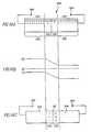
- the semiconductor device 340 is formed of a first region 342 consisting essentially of an amorphous semiconductor material, such as an amorphous silicon:hydrogen alloy or an amorphous silicon:fluorine:hydrogen alloy.
- the device 340 further includes a first field inducing body or layer 344, formed with a built-in charge, located in field effect proximity to the first region 342.
- a field inducing body which has a positive built-in charge such as the field inducing body 344 shown in Figure 14A
- a thin layer of an amorphous hydrogenated alloy of silicon nitride can be used.
- the positively charged field inducing layer 344 shifts the Fermi level of the material in region 342 toward the conduction band, increasing the number of electron charge carriers in that region and thus making it have n-type semiconductor properties.
- the device 340 further includes a second region 346 of material which has its Fermi level further away from the band edge toward which the material of the first region 342 has had its Fermi level shifted than the material of that first region.
- the Fermi level in a layer of the semiconductor material in the second region 346 parallel to a second field inducing body, or layer, 348 is shifted toward the valence band edge by means of that second field inducing body or layer 348.
- the field inducing body 348 is formed with a built-in negative charge and is placed in field effect proximity to the material of the second region 346.
- the material of both the first and second regions 342 and 346 are formed of the same continuous layer of amorphous semiconductor material.
- the amorphous semiconductor material in the proximity doped layer of region 342 has been proximity doped to form an n-type material and the proximity doped layer of region 346 has been proximity doped to be a p-type material, a p-n semiconductor junction is formed at the boundary between the two proximity doped layers. This p-n junction extends in a direction shown in Figure 14A so as to influence the conduction of current which lies within and runs parallel to the proximity doped layers induced by the field inducing layers 344 and 348.
- Figure 14B shows the energy levels of the conduction band edge E C and the valence band edge E v relative to Fermi level E F in the amorphous semiconductor material of the regions 342 and 346.
- the Fermi level in the region'342 is shifted toward the level of the conduction band edge E C and the Fermi level in the region 346 is shifted toward the level of the valence band edge E V .
- the conduction band edge E C and the valence band edge E v have to bend in the portions 350 and 352 of the semiconductor material near the junction between regions 342 and 346.
- This bending of the conduction and valence bend edges shown in Figure 14B correspondes to that which exists in a normal p-n junction diode of the type shown in Figure 14C.
- n-type material is normally comprised both of an excess of free electron relative to holes and of a non-conducting, positive charge which tends to shift the Fermi level toward the conduction band so as to create such an excess of free electrons.
- a p-type semiconductor material normally is comprised both of an excess of holes relative to free electron and of a non-conducting, negative charge which tends to shift the Fermi level toward the valence band edge so as to create such an excess of holes.
- impurity doped semiconductor materials such non-conducting charge is formed by charged doping impurity ions distributed throughout the semiconductor material.
- proximity doped semiconductors such non-conducting charge is formed by the built-in charge on field inducing layers.
- the field created by these charged regions creates a potential barrier which prevents diffusion of electrons from the n-type material and holes from the p-type material across the p-n junction unless those carriers have an energy greater than that of the potential barrier.
- the field created by such charged regions also creates a voltage induced, or drift, current in a direction opposite such diffusion current. At equilibrium, the drift current is equal to the diffusion current.
- a p-n junction has rectification properties because if a voltage is applied across its junction which increases the field across it, the barrier to diffusion will be increased, decreasing the amount of such diffusion exponentially. However, such an increase in the voltage across the junction will have a much smaller effect upon the drift current . As a result, such a diode operates as a reverse biased diode, in which the substantially only current is a small reverse current due to field induced drift. However if a voltage is applied in the opposite direction, so as to decrease the uncovered non-conducting charge in the regions near the junction, the barrier to diffusion across the junction will be decreased, greatly increasing the amount of diffusion current. In such a condition the junction is considered to be forward biased, and the amount of current it conducts is increased substantially. Thus, it can be seen that a p-n junction operates as a rectifier.
- the proximity doped p-n junction shown in Figure 14A operates similarly to the impurity doped p-n junction shown in Figure 14C even though the non-conducting charges which shift the Fermi levels in Figure 14A are placed in field inducing layers 344 and 348, rather than being distributed throughout the semiconductor material of the device, as in the case in Figure 14A.
- the junction device 370 is comprised of a substrate 372, which could be formed of a material such as glass.
- a source electrode 374 and a drain electrode 376 are formed of metal by traditional photolithographic techniques.
- a layer 378 of amorphous semiconductor material, such as an amorphous silicon:hydrogen alloy, is deposited between the source 374 and drain 376.
- a field inducing body, or layer, 380 is deposited over a portion of the layer 378 extending from the source 374 to a point located part way between the source 374 and the drain 376.
- the region of amorphous semiconductor material under the field inducing body 380 will have its Fermi level shifted.
- the field inducing layer 380 has a negative charge, such as can be achieved by depositing a layer of an amorphous hydrogenated alloy of silicon carbide.
- the portion of layer 378 beneath the field inducing layer 380 will have positive charge induced into it, making it a p-type semiconductor.
- a junction is created between a p-type semiconductor in the portion of the layer 380 below the field inducing layer 380 and the portion of layer 370 which is not covered by that field inducing layer.
- the energy of the conduction and valence band edges will be bent at the junction between those two regions and that junction will have rectifying properties.
- a semiconductor junction device 390 according to another aspect of the invention is shown.
- the device 390 is formed on a substrate 392, which can be formed of material such as glass.
- a first field inducing layer 394 is deposited upon the substrate 392, and then a second field inducing layer 396 is formed adjacent to the layer 394 upon the substrate 392.
- two electrodes 398 and 400 are formed over the field inducing layers 394 and 396, respectively, so as not to cover the junction between those two field inducing layers.
- a layer 402 of amorphous semiconductor material such as an amorphous silicon:hydrogen alloy, is deposited so as to extend between the electrodes 398 and 400 and so as to be in contact with the field inducing layers 394 and 396.
- a layer 404 of an insulating oxide is deposited on top of the layer 402.
- a variably chargeable body of material 406, preferably an electrode formed of metal is placed on top of the insulating layer 404, so as to extend between the electrode 398 and the junction between the field inducing layers 394 and 396.
- the field inducing layer 394 has a negative charge, which can be formed by using a material such as an amorphous hydrogenated alloy of silicon carbide. This induces a positive charge into the region 408 of the amorphous semiconductor material of layer 402, making the material of that region a p-type semiconductor.
- the field inducing layer 396 has a positive built-in charge, which can be formed by using a material such as an amorphous alloy of silicon nitride. This induces a negative charge into the region 410 of the layer 402, causing that material to have n-type characteristics. As a result, rectification will occur at the junction 412 formed between the two regions 408 and 410.
- the electrode 406 is located so as to be in field effect proximity with the p-type region 408 of the layer of amorphous semiconductor material 402.
- the amount of charge supplied to the electrode 406 through an electrical contact 412 is varied, the amount and direction in which that electrode shifts the Fermi level in the region 408 is correspondently varied. This makes it possible to effectively increase or decrease the p-type nature of the region 408, and thus alter the rectification characteristics of the junction 412.
- the proximity doped amorphous semiconductor junction devices of the present invention can be constructed and used in a number of different ways in addition to those shown in Figures 14 through 16.
- the ability to make proximity doped p-n junctions, such as shown in Figure 14A makes it possible to make bipolar transistors using proximity doped amorphous materials.
- proximity doped junction devices could be made by placing a proximity doped amorphous semiconductor in contact with a metal having a different Fermi level, so as to form a Schottky diode.
- the charged bodies used for proximity doping in the present invention need not be in the form of a layer, but also could be in the form of small regions of charged material deposited throughout the amorphous semiconductor material which they are used to proximity dope.
- the charged bodies used in the present invention can be made of a variety of materials, so long as they are either deposited with a net electrical charge or develop a net electrical charge upon their formation in the thin film transistor in which they are being used.
- the charged bodies of the present invention can be used to proximity dope amorphous semiconductor materials other than substantially intrinsic ones.
- proximity doping could be used with amorphous semiconductor materials which have undergone atomic impurity doping to make them p-type or n-type.
- the proximity doping of the present invention could be used to make such p-type materials more p-type and to make n-type materials more n-type.
- One use of such combined impurity and proximity doping would be to produce field effect transistor channel regions which were sufficiently n-type or p-type so as to conduct without the requirement of a gate voltage, and thus which would require a gate voltage to turn them off.
Landscapes
- Bipolar Transistors (AREA)
- Thin Film Transistor (AREA)
- Junction Field-Effect Transistors (AREA)
Applications Claiming Priority (2)
| Application Number | Priority Date | Filing Date | Title |
|---|---|---|---|
| US62514284A | 1984-06-27 | 1984-06-27 | |
| US625142 | 2000-07-25 |
Publications (2)
| Publication Number | Publication Date |
|---|---|
| EP0166261A2 true EP0166261A2 (de) | 1986-01-02 |
| EP0166261A3 EP0166261A3 (de) | 1989-01-11 |
Family
ID=24504772
Family Applications (1)
| Application Number | Title | Priority Date | Filing Date |
|---|---|---|---|
| EP85106685A Withdrawn EP0166261A3 (de) | 1984-06-27 | 1985-05-30 | Statisches Feld induzierte Halbleiteranordnungen |
Country Status (2)
| Country | Link |
|---|---|
| EP (1) | EP0166261A3 (de) |
| JP (1) | JPS6118178A (de) |
Cited By (10)
| Publication number | Priority date | Publication date | Assignee | Title |
|---|---|---|---|---|
| EP0258070A3 (de) * | 1986-07-25 | 1988-07-27 | SILICONIX Incorporated | Stromquelle mit einem durch das Verfahren auswählbaren Temperaturkoeffizienten |
| GB2222306A (en) * | 1988-08-23 | 1990-02-28 | Plessey Co Plc | Field effect transistor |
| EP0383743A3 (en) * | 1989-02-17 | 1990-11-22 | International Business Machines Corporation | Thin film transistor |
| EP0399737A1 (de) * | 1989-05-24 | 1990-11-28 | Xerox Corporation | Hochspannungsdünnschichttransistor |
| EP0419136A1 (de) * | 1989-09-13 | 1991-03-27 | Xerox Corporation | Elektrische Halbleiteranordnung mit einem internen Fehlerkorrekturteil |
| EP0444712A1 (de) * | 1990-03-02 | 1991-09-04 | Nippon Telegraph And Telephone Corporation | Mehrfachgatter-Dünnfilmtransistor |
| US5081513A (en) * | 1991-02-28 | 1992-01-14 | Xerox Corporation | Electronic device with recovery layer proximate to active layer |
| EP0570257A1 (de) * | 1992-05-15 | 1993-11-18 | Thomson-Csf | Feldeffekt-Halbleiteranordnung mit sekundärem Gate, Verfahren zur Herstellung und Verwendung in einer Matrix-Ansteuerungsanordnung |
| CN113169204A (zh) * | 2020-06-30 | 2021-07-23 | 深圳市大疆创新科技有限公司 | 图像传感器及其制作方法、搭载图像传感器的成像装置 |
| CN116190232A (zh) * | 2022-03-02 | 2023-05-30 | 北京超弦存储器研究院 | 半导体结构的制作方法及半导体结构 |
Family Cites Families (2)
| Publication number | Priority date | Publication date | Assignee | Title |
|---|---|---|---|---|
| JPS59117265A (ja) * | 1982-12-24 | 1984-07-06 | Toshiba Corp | 薄膜電界効果トランジスタ |
| JPS6066864A (ja) * | 1983-09-22 | 1985-04-17 | Seiko Instr & Electronics Ltd | Mis型薄膜トランジスタ |
-
1985
- 1985-05-30 EP EP85106685A patent/EP0166261A3/de not_active Withdrawn
- 1985-06-27 JP JP60141478A patent/JPS6118178A/ja active Pending
Cited By (13)
| Publication number | Priority date | Publication date | Assignee | Title |
|---|---|---|---|---|
| EP0258070A3 (de) * | 1986-07-25 | 1988-07-27 | SILICONIX Incorporated | Stromquelle mit einem durch das Verfahren auswählbaren Temperaturkoeffizienten |
| GB2222306B (en) * | 1988-08-23 | 1992-08-12 | Plessey Co Plc | Field effect transistor devices |
| GB2222306A (en) * | 1988-08-23 | 1990-02-28 | Plessey Co Plc | Field effect transistor |
| EP0383743A3 (en) * | 1989-02-17 | 1990-11-22 | International Business Machines Corporation | Thin film transistor |
| EP0399737A1 (de) * | 1989-05-24 | 1990-11-28 | Xerox Corporation | Hochspannungsdünnschichttransistor |
| EP0419136A1 (de) * | 1989-09-13 | 1991-03-27 | Xerox Corporation | Elektrische Halbleiteranordnung mit einem internen Fehlerkorrekturteil |
| EP0444712A1 (de) * | 1990-03-02 | 1991-09-04 | Nippon Telegraph And Telephone Corporation | Mehrfachgatter-Dünnfilmtransistor |
| US5124769A (en) * | 1990-03-02 | 1992-06-23 | Nippon Telegraph And Telephone Corporation | Thin film transistor |
| US5081513A (en) * | 1991-02-28 | 1992-01-14 | Xerox Corporation | Electronic device with recovery layer proximate to active layer |
| EP0570257A1 (de) * | 1992-05-15 | 1993-11-18 | Thomson-Csf | Feldeffekt-Halbleiteranordnung mit sekundärem Gate, Verfahren zur Herstellung und Verwendung in einer Matrix-Ansteuerungsanordnung |
| FR2691289A1 (fr) * | 1992-05-15 | 1993-11-19 | Thomson Csf | Dispositif semiconducteur à effet de champ, procédé de réalisation et application à un dispositif à commande matricielle. |
| CN113169204A (zh) * | 2020-06-30 | 2021-07-23 | 深圳市大疆创新科技有限公司 | 图像传感器及其制作方法、搭载图像传感器的成像装置 |
| CN116190232A (zh) * | 2022-03-02 | 2023-05-30 | 北京超弦存储器研究院 | 半导体结构的制作方法及半导体结构 |
Also Published As
| Publication number | Publication date |
|---|---|
| JPS6118178A (ja) | 1986-01-27 |
| EP0166261A3 (de) | 1989-01-11 |
Similar Documents
| Publication | Publication Date | Title |
|---|---|---|
| US4746960A (en) | Vertical depletion-mode j-MOSFET | |
| US7655515B2 (en) | Lateral DMOS structure with lateral extension structure for reduced charge trapping in gate oxide | |
| US4882295A (en) | Method of making a double injection field effect transistor | |
| US5274259A (en) | High voltage transistor | |
| US4866495A (en) | High power MOSFET and integrated control circuit therefor for high-side switch application | |
| KR101791713B1 (ko) | 전계 효과 트랜지스터 및 반도체 장치 | |
| US5023678A (en) | High power MOSFET and integrated control circuit therefor for high-side switch application | |
| US6943408B2 (en) | Semiconductor bidirectional switching device | |
| US4752814A (en) | High voltage thin film transistor | |
| US4755857A (en) | Heterostructure semiconductor device | |
| EP0097442A2 (de) | Lateraler bi-direktionaler Feldeffekttransistor mit einem Einschnitt | |
| US6118149A (en) | Trench gate MOSFET | |
| JPH0656888B2 (ja) | 半導体装置 | |
| EP0638938A2 (de) | SOI-Transistor mit verbesserer Hochquelle | |
| KR940010367A (ko) | 반도체장치 및 그 제조방법 | |
| US4070687A (en) | Composite channel field effect transistor and method of fabrication | |
| GB2089118A (en) | Field-effect semiconductor device | |
| US4743951A (en) | Field effect transistor | |
| JPH06104438A (ja) | 薄膜トランジスタ | |
| US3590343A (en) | Resonant gate transistor with fixed position electrically floating gate electrode in addition to resonant member | |
| JPS6118178A (ja) | 近接ドープされた半導体デバイス | |
| US3585463A (en) | Complementary enhancement-type mos transistors | |
| Richman | The effect of gold doping upon the characteristics of MOS field-effect transistors with applied substrate voltage | |
| US5107314A (en) | Gallium antimonide field-effect transistor | |
| US5529940A (en) | Method of manufacturing a vertical MOSFET having a gate electrode of polycrystalline silicon |
Legal Events
| Date | Code | Title | Description |
|---|---|---|---|
| PUAI | Public reference made under article 153(3) epc to a published international application that has entered the european phase |
Free format text: ORIGINAL CODE: 0009012 |
|
| AK | Designated contracting states |
Designated state(s): AT BE CH DE FR GB IT LI LU NL SE |
|
| PUAL | Search report despatched |
Free format text: ORIGINAL CODE: 0009013 |
|
| AK | Designated contracting states |
Kind code of ref document: A3 Designated state(s): AT BE CH DE FR GB IT LI LU NL SE |
|
| STAA | Information on the status of an ep patent application or granted ep patent |
Free format text: STATUS: THE APPLICATION IS DEEMED TO BE WITHDRAWN |
|
| 18D | Application deemed to be withdrawn |
Effective date: 19881201 |
|
| RIN1 | Information on inventor provided before grant (corrected) |
Inventor name: SHUR, MICHAEL Inventor name: GUHA, SUBHENDU Inventor name: OVSHINSKY, STANFORD R. Inventor name: HACK, MICHAEL G. |