EP0445505A1 - Cellule de base pour un dispositif de circuit prédiffusé du type "mer de portes" - Google Patents
Cellule de base pour un dispositif de circuit prédiffusé du type "mer de portes" Download PDFInfo
- Publication number
- EP0445505A1 EP0445505A1 EP19910100380 EP91100380A EP0445505A1 EP 0445505 A1 EP0445505 A1 EP 0445505A1 EP 19910100380 EP19910100380 EP 19910100380 EP 91100380 A EP91100380 A EP 91100380A EP 0445505 A1 EP0445505 A1 EP 0445505A1
- Authority
- EP
- European Patent Office
- Prior art keywords
- effect transistors
- mos field
- rows
- gate
- channel type
- Prior art date
- Legal status (The legal status is an assumption and is not a legal conclusion. Google has not performed a legal analysis and makes no representation as to the accuracy of the status listed.)
- Granted
Links
Images


Classifications
-
- H—ELECTRICITY
- H10—SEMICONDUCTOR DEVICES; ELECTRIC SOLID-STATE DEVICES NOT OTHERWISE PROVIDED FOR
- H10D—INORGANIC ELECTRIC SEMICONDUCTOR DEVICES
- H10D84/00—Integrated devices formed in or on semiconductor substrates that comprise only semiconducting layers, e.g. on Si wafers or on GaAs-on-Si wafers
- H10D84/90—Masterslice integrated circuits
- H10D84/903—Masterslice integrated circuits comprising field effect technology
- H10D84/907—CMOS gate arrays
-
- H—ELECTRICITY
- H10—SEMICONDUCTOR DEVICES; ELECTRIC SOLID-STATE DEVICES NOT OTHERWISE PROVIDED FOR
- H10D—INORGANIC ELECTRIC SEMICONDUCTOR DEVICES
- H10D84/00—Integrated devices formed in or on semiconductor substrates that comprise only semiconducting layers, e.g. on Si wafers or on GaAs-on-Si wafers
- H10D84/90—Masterslice integrated circuits
- H10D84/996—Masterslice integrated circuits using combined field effect technology and bipolar technology
-
- H—ELECTRICITY
- H10—SEMICONDUCTOR DEVICES; ELECTRIC SOLID-STATE DEVICES NOT OTHERWISE PROVIDED FOR
- H10D—INORGANIC ELECTRIC SEMICONDUCTOR DEVICES
- H10D84/00—Integrated devices formed in or on semiconductor substrates that comprise only semiconducting layers, e.g. on Si wafers or on GaAs-on-Si wafers
- H10D84/90—Masterslice integrated circuits
- H10D84/903—Masterslice integrated circuits comprising field effect technology
- H10D84/907—CMOS gate arrays
- H10D84/909—Microarchitecture
- H10D84/935—Degree of specialisation for implementing specific functions
- H10D84/937—Implementation of digital circuits
- H10D84/938—Implementation of memory functions
Definitions
- the invention relates to a basic cell for a channelless gate array arrangement ("Sea of Gate” (SOG) array) in a technology combining CMOS and bipolar technology, according to the preamble of claim 1 and the use of such a basic cell for construction a SOG array.
- SOG channelless gate array arrangement
- An SOG array is the regular arrangement of basic cells that is made up of non-interconnected components. A circuit is implemented by configuring contact hole and metal masks. In contrast to classic gate arrays, SOG arrays do not have any reserved channels for wiring; rather, the metallization can also be carried out via the individual components. This type of wiring therefore requires at least two levels of metal wiring.
- the BICMOS-SOG array consisting of BICMOS basic cells, which is disclosed by the above-mentioned publication, represents a universal array with a wide range of applications.
- the characteristic of this known array is the construction from a single basic cell, which is not based on a special circuit structure, e.g. B. static NAND logic is optimized, but allows different design styles. In addition to static logic, such a basic structure also enables the implementation of dynamic stages and memories, for example SRAMs.
- the object of the present invention is therefore to provide a basic cell of the type mentioned at the outset, which covers a wide range of applications, is compact and has a high degree of connectivity.
- the invention consists in the fact that two rows of NMOS field-effect transistors and one row of PMOS field-effect transistors are in opposite order in the order listed here Connect the sides of a BICMOS component, with a certain division into gate-insulated and oxide-insulated field-effect transistors.
- gate-insulated field effect transistors are field effect transistors whose gates are arranged on a common n- or p-doped area, a field effect transistor being implemented by each gate.
- the middle field effect transistors can be controlled by three neighboring field effect transistors by placing its gate at a corresponding potential such that the two outer field effect transistors are electrically insulated from one another.
- each oxide-insulated is assigned its own n- or p-doped region, which are electrically insulated from one another, for example by silicon dioxide (SiO2).
- This special arrangement of the transistor rows means that an SOG array constructed with such a basic cell according to the invention can be used universally. Static and dynamic logic components as well as RAM and ROM memory as well as input and output driver stages can be implemented.
- the special configuration of the gate electrodes with their staggered connection regions achieves a high degree of connectivity, because if, for example, a gate connection is covered by an interconnect, the corresponding gate can nevertheless be contacted via its second gate connection.
- a high permeability is also given by the fact that, for example, opposite rows can be connected to one another across the BICMOS component arranged in the central area of the basic cell, without thereby interfering with the function of the BICMOS component.
- connection areas of the gate electrodes of the MOS field-effect transistors in each case of the first and third rows are offset in the same direction, while those connection areas of the gate electrodes of the MOS field-effect transistors in each case of the second row are related to those of the MOS field-effect transistors the first and third rows are offset in opposite directions. This further improves the universal applicability of the SOG array arrangement constructed with such a basic cell.
- the permeability is improved in that, according to another advantageous development of the invention, the gate electrodes with their connection areas of the MOS field-effect transistors of the first, second and third rows are arranged mirror-symmetrically with respect to the central area.
- the channel width of the field effect transistors of the third series is approximately twice as large as that of the field effect transistors of the second series.
- the channel width of the field effect transistors in the first row is approximately half that of the field effect transistors in the second row.
- the basic cell according to the invention can advantageously be used to construct an SOG array arrangement consisting of rows and columns.
- its rows are made up of basic cells strung together in the X direction.
- Such rows strung together in the Y direction then result in the entire SOG array, in which case there is in particular the advantageous possibility of, for example, realizing a CMOS component over two adjacent rows in such a way that the third and fourth rows of the two adjacent basic cells are used .
- a particularly preferred development of the SOG array arrangement results from the structure of the SOG array with 29 rows and 125 columns.
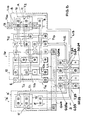
- the circuit diagram of FIG. 2 corresponds to the layout of a basic cell according to the invention shown in FIG. 1, which is why both figures are explained together.
- the rectangular shape of the basic cell can be seen with a size of about 175 x 50 microns.
- a BICMOS component is arranged in a central area 1 of this basic cell and is divided into two areas 1a and 1b in the X direction.
- a bipolar transistor T is provided in the first region 1 a, which is constructed in accordance with the layout from a collector region 8 with its collector connection region 9, the base region 10 and the emitter region 11. According to the layout, the collector connection region 9, the base region 10 and the emitter region 11 are arranged in the Y direction.
- the area 1b carries the CMOS part of the BICMOS component and comprises the MOS field effect transistors T11, T12, T13, T14 and T15. These MOS field-effect transistors are arranged in the corner points and in the diagonal intersection of this second region 1b.
- the transistors T11, T13 and T14 are of the p-channel type and are therefore arranged according to the layout in an n-doped region 12, for example a well, while the remaining two transistors T12 and T15 are n-channel transistors which are in a p -doped area are arranged. Furthermore, it can be seen from the layout according to FIG.
- These MOS field-effect transistors of the first rows 2 and 3 are constructed from source-drain regions SD21 to SD25 and SD31 to SD35 which are extended in the Y direction.
- the associated gate electrodes G21 to G25 and G31 to G35 have an oblique course with respect to the Y direction and are guided over the associated source-drain regions SD21 to SD25 and SD31 to SD35. Since these gate electrodes are provided on both sides with a connection area G21a and G21b to G25a and G25b or G31a and G31b to G35a and G35b, this gate connection area is offset with respect to the Y direction.
- These second rows 2 and 3 of MOS field effect transistors are followed by a second row 4 and 5 of gate-isolated MOS field effect transistors T41 to T45 and T51 to T55 of the n-channel type, which are also lined up in the X direction.
- These gate-insulated MOS field effect transistors have a common area SD4 or SD5, while the gate electrode G41 to G45 and G51 to G55 assigned to each MOS field effect transistor is guided obliquely over the associated area SD4 or SD5.
- These named gate electrodes also each have a gate connection region G41a and G41b to G45a and G45b or G51a and G51b to G55a and G55b on both sides. As a result, these gate connection regions are also offset with respect to the Y direction. Contacts 17 and 18 to the p-region are provided between the gate connection regions.
- the second rows 4 and 5 are followed by a last row of gate-isolated MOS field-effect transistors T61 to T65 and T71 to T75 of the p-channel type, which are lined up in the X direction.
- these MOS field-effect transistors are arranged in an n-doped region 13 or 14.
- These MOS field-effect transistors of rows 6 and 7 also have a common area SD6 and SD7, respectively.
- the gate electrodes G61 to G65 and G71 to G75 are each guided obliquely with respect to the Y direction over the associated area SD6 or SD7.
- these gate electrodes are each provided with two gate connection regions G61a and G61b to G65a and G65b or G71a and G71b to G75a and G75b. This also results in an offset arrangement of the gate connection regions with respect to the Y direction. Furthermore, contacts 15 and 16 to the n-regions 13 and 14 are arranged between the gate connection areas.
- the gate electrodes of the respective MOS field-effect transistors belonging to a row are arranged parallel to one another.
- the gate electrodes of the first and third rows 2 and 6 or 3 and 7 each have a parallel profile, while those of the second rows 4 and 5 run in opposite directions.
- the gate electrodes of the first, second and third rows 2, 3, 4, 5, 6 and 7 are arranged mirror-symmetrically with respect to the central region 1.
- FIG. 3 shows an example of a layout for vertical wiring of the first rows 2 and 3 of a basic cell according to FIG. 1, but only the central region 1 and the adjoining first rows 2 and 3 of the MOS field-effect transistors T21 to T25 and T31 to T35 are shown.
- the individual components Metallization levels made of aluminum necessary.
- the interconnects L2 of the second metallization level are drawn with dots compared to those of the first metallization level.
- corresponding contact areas K2 are also arranged between the gate connection area G33a, G34a and G35a and the second area 1b. These contact areas K1 and K2 are each connected to the adjacent gate connection areas via an interconnect L1, while the contact areas K1 and K2 opposite each other in the Y direction are each connected via an interconnect L2 belonging to the second metallization level.
- This wiring to the conductor tracks L2 of the second metallization level is designed in such a way that the usability of the MOS field-effect transistors T11 to T15 is not restricted, since contact regions for the source-drain regions and also for the gate electrodes of these transistors are shown in accordance with this layout and can be wired by means of the first metallization level without any restriction through the interconnects L2.
- FIG. 4 shows a layout of a NAND gate with two inputs in accordance with the circuit diagram and the corresponding symbol of FIG. 5.
- This NAND gate is with the MOS transistors T51 to T53 of the series 5 and the MOS field effect transistors T71 to T73 of the series 7 realized, therefore only such a section of the basic cell is drawn.
- the reference symbols for the MOS field-effect transistors in accordance with the circuit diagram correspond to those in the layout, so that simple assignment is possible. It can be seen from this that the MOS field effect transistors T51, T52, T71 and T72 are used to implement the NAND gate, while the MOS field effect transistors T53 and T73 are used for isolation.
- interconnect L3 for the ground connection GND
- interconnect L4 for connection to the operating voltage source V DD
- These two interconnects L3 and L4 run in the X direction and partially cover the areas SD5 and SD7. The rest of the wiring is done on the first level of metallization.
- the n-doped region 14 is connected to the operating voltage source V DD via contact K1, while the p-doped region in the vicinity of the region SD6 is connected to ground potential GND via the contacts K2, K3.
- output A and the two inputs E1 and E2 are designated in the layout.
- FIG. 6 now shows the layout of a static RAM memory cell, the circuit diagram of which is shown in FIG.
- This RAM memory cell is implemented with the MOS field effect transistors T61, T62, T41, T42, T43, T22 and T23 of the rows 6, 4 and 2.
- the layout therefore only shows the corresponding section from the basic cell according to FIG. 2.
- a conductor track L5 of the second metallization level is drawn in parallel over the area SD6 and is furthermore each designated with a solid diagonal cross contact areas 15a and 15b connected. Such contact areas, denoted by a solid diagonal cross, establish the connection between the second and the first metallization level.
- those contact areas which are denoted by a diagonally drawn cross form the connection between the first metallization level and the gate electrodes or the diffusion areas.
- the gate connection region G62a of the field effect transistor T62 is contacted with the first metallization level and is connected via a conductive path of this first metallization level to a contact K3, which covers the area underneath SD6 contacted.
- the gate G62 of the field effect transistor T62 via its gate connection region G62b is likewise via an interconnect of the first metallization level both with the region SD4 and with the gate electrode G23 of the field effect transistor T23 via its gate connection region G23a and with the source drain - Area SD22 of the MOS field-effect transistor T22 connected, compare the circuit diagram in FIG. 7.
- a conductor track L6 of the second metallization level also leads in parallel over the area SD4 of the MOS field-effect transistors of the second row 4, which serves as a word line.
- This interconnect L6 is also connected via the contact regions 17a and 17b connecting the two metallization levels to the gate connection regions G43a and G42a, to which the gate electrodes G43 and G42 of the MOS field-effect transistors T43 and T42 are assigned.
- the connection between this contact region 17a or 17b and the gate connection region G43a or G41a establishes an interconnect of the first metallization level.
- a third interconnect L7 of the second metallization level is guided in parallel over the MOS field-effect transistors of the first row 2 and serves as a reference potential GND. Furthermore, this interconnect L7 leads to a contact region 17c which connects the two metallization levels and which is connected via an interconnect of the first metallization level to the gate G42 via its gate connection region G42b.
- the associated MOS field effect transistor T42 serves to isolate the two adjacent MOS field effect transistors T41 and T43.
- the two lines L8 and L9 of the first metallization level represent the bit or bit Lines.
- FIG. 8 finally shows the layout of a BICMOS driver stage according to the circuit diagram of FIG. 9.
- This layout only shows the central area 1 of a basic cell and the MOS field effect transistors T34 and T35 of the first row 3 and the first area 1a 'of a central area 1 'an adjacent basic cell.
- the two npn transistors of the first regions 1a and 1a ' are used as output stage transistors T1, T2 according to the circuit diagram according to FIG.
- the two P-channel field effect transistors T11 and T14 of the second region 1b are connected in parallel on the first metallization level and represent the transistor T11 / T14 according to the circuit in FIG. 9.
- the two MOS field effect transistors T34 and T35 are wired in parallel in the first metallization level 9 shows the transistor T24 / T25.
- the two gate connection regions G34a and G35a are connected via an interconnect of the first metallization level
- the two source-drain regions SD34 and SD35 are connected via the two lines L12 and L13.
- a first interconnect L10 of the second metallization level is used to supply the operating voltage source V DD and a second interconnect L11 of the second metallization level is used as the reference potential GND.
- input E and output A are also designated in the layout according to FIG.
- Such a BICMOS driver stage can now be implemented together with logic units on a SOG array constructed with the basic cell according to the invention, for example a shift register with two BICMOS driver stages at the output.
- Such an SOG array can be constructed, for example, from 29 rows and 125 columns of such basic cells according to the invention, the rows being built up from basic cells arranged in a row.
- the size of such an SOG array is, for example, 6.25 x 5.075 mm, which corresponds to an area of 31.72 mm2.
- This SOG array then contains 126 875 MOS field-effect transistors, of which 79 750 NMOS field-effect transistors and 43 500 PMOS field-effect transistors, and 3625 NPN transistors.
- the delay times for CMOS inverters are approx. 300 ps if this inverter is loaded with an identical inverter.
- a BICMOS driver stage according to FIG. 8 requires approx. 600 ps.
Landscapes
- Design And Manufacture Of Integrated Circuits (AREA)
Applications Claiming Priority (2)
| Application Number | Priority Date | Filing Date | Title |
|---|---|---|---|
| DE4002780A DE4002780C2 (de) | 1990-01-31 | 1990-01-31 | Basiszelle für eine kanallose Gate-Array-Anordnung |
| DE4002780 | 1990-01-31 |
Publications (2)
| Publication Number | Publication Date |
|---|---|
| EP0445505A1 true EP0445505A1 (fr) | 1991-09-11 |
| EP0445505B1 EP0445505B1 (fr) | 1994-11-30 |
Family
ID=6399115
Family Applications (1)
| Application Number | Title | Priority Date | Filing Date |
|---|---|---|---|
| EP91100380A Expired - Lifetime EP0445505B1 (fr) | 1990-01-31 | 1991-01-15 | Cellule de base pour un dispositif de circuit prédiffusé du type "mer de portes" |
Country Status (2)
| Country | Link |
|---|---|
| EP (1) | EP0445505B1 (fr) |
| DE (2) | DE4002780C2 (fr) |
Cited By (1)
| Publication number | Priority date | Publication date | Assignee | Title |
|---|---|---|---|---|
| EP0683524A1 (fr) * | 1994-05-10 | 1995-11-22 | Texas Instruments Incorporated | Cellule de base pour matrices pré-diffusées BICMOS et CMOS |
Citations (1)
| Publication number | Priority date | Publication date | Assignee | Title |
|---|---|---|---|---|
| EP0102644A2 (fr) * | 1982-09-06 | 1984-03-14 | Hitachi, Ltd. | Circuit intégré semi-conducteur |
Family Cites Families (5)
| Publication number | Priority date | Publication date | Assignee | Title |
|---|---|---|---|---|
| IT1191188B (it) * | 1982-04-15 | 1988-02-24 | Cselt Centro Studi Lab Telecom | Cella elementare per reti di porte logiche a circuito integrato |
| JPH0669142B2 (ja) * | 1983-04-15 | 1994-08-31 | 株式会社日立製作所 | 半導体集積回路装置 |
| JPS6035532A (ja) * | 1983-07-29 | 1985-02-23 | Fujitsu Ltd | マスタスライス集積回路装置 |
| JPH0831581B2 (ja) * | 1988-02-19 | 1996-03-27 | 株式会社東芝 | 半導体装置 |
| JPH01256149A (ja) * | 1988-04-06 | 1989-10-12 | Hitachi Ltd | ゲートアレイ集積回路 |
-
1990
- 1990-01-31 DE DE4002780A patent/DE4002780C2/de not_active Expired - Fee Related
-
1991
- 1991-01-15 EP EP91100380A patent/EP0445505B1/fr not_active Expired - Lifetime
- 1991-01-15 DE DE59103611T patent/DE59103611D1/de not_active Expired - Fee Related
Patent Citations (1)
| Publication number | Priority date | Publication date | Assignee | Title |
|---|---|---|---|---|
| EP0102644A2 (fr) * | 1982-09-06 | 1984-03-14 | Hitachi, Ltd. | Circuit intégré semi-conducteur |
Non-Patent Citations (3)
| Title |
|---|
| PATENT ABSTRACTS OF JAPAN, Band 12, Nr. 412 (E-676)[3259], 31. Oktober 1988; & JP-A-63 150 935 (SEIKO EPSON CORP.) 23-06-1988 * |
| PATENT ABSTRACTS OF JAPAN, Band 6, Nr. 251 (E-147)[1129], 10. Dezember 1982; & JP-A-57 148 363 (TOKYO SHIBAURA DENKI K.K.) 13-09-1982 * |
| PROCEEDINGS OF THE IEEE 1989 CUSTOM INTEGRATED CIRCUITS CONFERENCE, San Diego, CA, 15. - 18. Mai 1989, Seiten 8.3.1-8.3.4; A.E. GAMAL et al.: "BINMOS: A basic cell for BiCMOS sea-of-gates" * |
Cited By (2)
| Publication number | Priority date | Publication date | Assignee | Title |
|---|---|---|---|---|
| EP0683524A1 (fr) * | 1994-05-10 | 1995-11-22 | Texas Instruments Incorporated | Cellule de base pour matrices pré-diffusées BICMOS et CMOS |
| US5591995A (en) * | 1994-05-10 | 1997-01-07 | Texas Instruments, Incorporated | Base cell for BiCMOS and CMOS gate arrays |
Also Published As
| Publication number | Publication date |
|---|---|
| DE4002780C2 (de) | 1995-01-19 |
| EP0445505B1 (fr) | 1994-11-30 |
| DE59103611D1 (de) | 1995-01-12 |
| DE4002780A1 (de) | 1991-08-01 |
Similar Documents
| Publication | Publication Date | Title |
|---|---|---|
| DE69524804T2 (de) | Basiszelle für BICMOS und CMOS-Gate-Arrays | |
| DE69427599T2 (de) | Basiszelle für ein Gate-Array mit doppeltem Puffer | |
| EP0051693B1 (fr) | Mémoire morte électriquement commutable | |
| DE69232136T2 (de) | Basiszellen-architektur für maskenprogrammierbare gattermatrix | |
| DE3750770T2 (de) | Integrierte Schaltung in Hauptscheibentechnik. | |
| DE3712178C2 (fr) | ||
| EP0280176A1 (fr) | Cellule de base pour matrice de portes | |
| DE2556274A1 (de) | Logische schaltung hoher schaltungsdichte | |
| DE69517693T2 (de) | Standardzellenbibliothek für den Entwurf von integrierten Schaltungen | |
| DE3872737T2 (de) | Verfahren zur kombinierung von "gate array"-schaltungen mit standardschaltungen auf ein gemeinsames halbleiterplaettchen. | |
| DE3486077T2 (de) | Integrierte halbleiterschaltungsanordnung. | |
| DE69009626T2 (de) | Masterslice-Halbleitervorrichtung. | |
| DE69920121T2 (de) | Wortleitungstreiberschaltung mit ringförmiger Vorrichtung | |
| DE3751607T2 (de) | Stromversorgungsleitungen in einer integrierten Halbleiterschaltung. | |
| DE69230019T2 (de) | Anordnung von Transistoren zur Fertigung einer Basiszelle für eine integrierte Masterslice-Halbleiteranordnung und integrierte Masterslice-Halbleiteranordnung | |
| DE2823555A1 (de) | Zellenfoermige integrierte schaltung | |
| EP0001209A1 (fr) | Circuit semi-conducteur intégré | |
| EP0166027B1 (fr) | Cellule élémentaire réalisée en technique C-MOS | |
| EP0445505B1 (fr) | Cellule de base pour un dispositif de circuit prédiffusé du type "mer de portes" | |
| DE19731714A1 (de) | Integrierte Halbleiterschaltungseinrichtung | |
| DE2539967C2 (de) | Logikgrundschaltung | |
| EP0082208B1 (fr) | Circuit de commutation intégré du type CMOS | |
| DE19735231C2 (de) | Neuronales MOSFET-Modul | |
| DE68923580T2 (de) | Integrierte Halbleiterschaltungsanordnung. | |
| DE19749599C2 (de) | Takttreiberschaltung und integrierte Halbleiterschaltungseinrichtung mit Makrozellenlayoutbereichen |
Legal Events
| Date | Code | Title | Description |
|---|---|---|---|
| PUAI | Public reference made under article 153(3) epc to a published international application that has entered the european phase |
Free format text: ORIGINAL CODE: 0009012 |
|
| AK | Designated contracting states |
Kind code of ref document: A1 Designated state(s): DE FR GB IT |
|
| 17P | Request for examination filed |
Effective date: 19910823 |
|
| RIN1 | Information on inventor provided before grant (corrected) |
Inventor name: SCHARDEIN, WERNER, DR. Inventor name: ROTHERMEL, ALBRECHT, DR. Inventor name: ESSER, WINFRIED Inventor name: TROESTER, GERHARD, DR. |
|
| RAP1 | Party data changed (applicant data changed or rights of an application transferred) |
Owner name: TEMIC TELEFUNKEN MICROELECTRONIC GMBH |
|
| 17Q | First examination report despatched |
Effective date: 19940506 |
|
| GRAA | (expected) grant |
Free format text: ORIGINAL CODE: 0009210 |
|
| AK | Designated contracting states |
Kind code of ref document: B1 Designated state(s): DE FR GB IT |
|
| GBT | Gb: translation of ep patent filed (gb section 77(6)(a)/1977) |
Effective date: 19941206 |
|
| REF | Corresponds to: |
Ref document number: 59103611 Country of ref document: DE Date of ref document: 19950112 |
|
| ITF | It: translation for a ep patent filed | ||
| PGFP | Annual fee paid to national office [announced via postgrant information from national office to epo] |
Ref country code: DE Payment date: 19950306 Year of fee payment: 5 |
|
| ET | Fr: translation filed | ||
| PLBE | No opposition filed within time limit |
Free format text: ORIGINAL CODE: 0009261 |
|
| STAA | Information on the status of an ep patent application or granted ep patent |
Free format text: STATUS: NO OPPOSITION FILED WITHIN TIME LIMIT |
|
| 26N | No opposition filed | ||
| PGFP | Annual fee paid to national office [announced via postgrant information from national office to epo] |
Ref country code: GB Payment date: 19951221 Year of fee payment: 6 |
|
| PGFP | Annual fee paid to national office [announced via postgrant information from national office to epo] |
Ref country code: FR Payment date: 19960116 Year of fee payment: 6 |
|
| PG25 | Lapsed in a contracting state [announced via postgrant information from national office to epo] |
Ref country code: DE Effective date: 19961001 |
|
| PG25 | Lapsed in a contracting state [announced via postgrant information from national office to epo] |
Ref country code: GB Effective date: 19970115 |
|
| GBPC | Gb: european patent ceased through non-payment of renewal fee |
Effective date: 19970115 |
|
| PG25 | Lapsed in a contracting state [announced via postgrant information from national office to epo] |
Ref country code: FR Effective date: 19970930 |
|
| REG | Reference to a national code |
Ref country code: FR Ref legal event code: ST |
|
| PG25 | Lapsed in a contracting state [announced via postgrant information from national office to epo] |
Ref country code: IT Free format text: LAPSE BECAUSE OF NON-PAYMENT OF DUE FEES;WARNING: LAPSES OF ITALIAN PATENTS WITH EFFECTIVE DATE BEFORE 2007 MAY HAVE OCCURRED AT ANY TIME BEFORE 2007. THE CORRECT EFFECTIVE DATE MAY BE DIFFERENT FROM THE ONE RECORDED. Effective date: 20050115 |