EP0446079B1 - Industrial material with fluorine passivated film and process of manufacturing the same - Google Patents
Industrial material with fluorine passivated film and process of manufacturing the same Download PDFInfo
- Publication number
- EP0446079B1 EP0446079B1 EP91302016A EP91302016A EP0446079B1 EP 0446079 B1 EP0446079 B1 EP 0446079B1 EP 91302016 A EP91302016 A EP 91302016A EP 91302016 A EP91302016 A EP 91302016A EP 0446079 B1 EP0446079 B1 EP 0446079B1
- Authority
- EP
- European Patent Office
- Prior art keywords
- nickel
- film
- substrate
- fluorine
- nickel alloy
- Prior art date
- Legal status (The legal status is an assumption and is not a legal conclusion. Google has not performed a legal analysis and makes no representation as to the accuracy of the status listed.)
- Expired - Lifetime
Links
Images


Classifications
-
- H—ELECTRICITY
- H10—SEMICONDUCTOR DEVICES; ELECTRIC SOLID-STATE DEVICES NOT OTHERWISE PROVIDED FOR
- H10P—GENERIC PROCESSES OR APPARATUS FOR THE MANUFACTURE OR TREATMENT OF DEVICES COVERED BY CLASS H10
- H10P72/00—Handling or holding of wafers, substrates or devices during manufacture or treatment thereof
- H10P72/70—Handling or holding of wafers, substrates or devices during manufacture or treatment thereof for supporting or gripping
- H10P72/74—Handling or holding of wafers, substrates or devices during manufacture or treatment thereof for supporting or gripping using temporarily an auxiliary support
-
- C—CHEMISTRY; METALLURGY
- C23—COATING METALLIC MATERIAL; COATING MATERIAL WITH METALLIC MATERIAL; CHEMICAL SURFACE TREATMENT; DIFFUSION TREATMENT OF METALLIC MATERIAL; COATING BY VACUUM EVAPORATION, BY SPUTTERING, BY ION IMPLANTATION OR BY CHEMICAL VAPOUR DEPOSITION, IN GENERAL; INHIBITING CORROSION OF METALLIC MATERIAL OR INCRUSTATION IN GENERAL
- C23C—COATING METALLIC MATERIAL; COATING MATERIAL WITH METALLIC MATERIAL; SURFACE TREATMENT OF METALLIC MATERIAL BY DIFFUSION INTO THE SURFACE, BY CHEMICAL CONVERSION OR SUBSTITUTION; COATING BY VACUUM EVAPORATION, BY SPUTTERING, BY ION IMPLANTATION OR BY CHEMICAL VAPOUR DEPOSITION, IN GENERAL
- C23C28/00—Coating for obtaining at least two superposed coatings either by methods not provided for in a single one of groups C23C2/00 - C23C26/00 or by combinations of methods provided for in subclasses C23C and C25C or C25D
- C23C28/02—Coating for obtaining at least two superposed coatings either by methods not provided for in a single one of groups C23C2/00 - C23C26/00 or by combinations of methods provided for in subclasses C23C and C25C or C25D only coatings only including layers of metallic material
- C23C28/021—Coating for obtaining at least two superposed coatings either by methods not provided for in a single one of groups C23C2/00 - C23C26/00 or by combinations of methods provided for in subclasses C23C and C25C or C25D only coatings only including layers of metallic material including at least one metal alloy layer
-
- C—CHEMISTRY; METALLURGY
- C23—COATING METALLIC MATERIAL; COATING MATERIAL WITH METALLIC MATERIAL; CHEMICAL SURFACE TREATMENT; DIFFUSION TREATMENT OF METALLIC MATERIAL; COATING BY VACUUM EVAPORATION, BY SPUTTERING, BY ION IMPLANTATION OR BY CHEMICAL VAPOUR DEPOSITION, IN GENERAL; INHIBITING CORROSION OF METALLIC MATERIAL OR INCRUSTATION IN GENERAL
- C23C—COATING METALLIC MATERIAL; COATING MATERIAL WITH METALLIC MATERIAL; SURFACE TREATMENT OF METALLIC MATERIAL BY DIFFUSION INTO THE SURFACE, BY CHEMICAL CONVERSION OR SUBSTITUTION; COATING BY VACUUM EVAPORATION, BY SPUTTERING, BY ION IMPLANTATION OR BY CHEMICAL VAPOUR DEPOSITION, IN GENERAL
- C23C28/00—Coating for obtaining at least two superposed coatings either by methods not provided for in a single one of groups C23C2/00 - C23C26/00 or by combinations of methods provided for in subclasses C23C and C25C or C25D
- C23C28/02—Coating for obtaining at least two superposed coatings either by methods not provided for in a single one of groups C23C2/00 - C23C26/00 or by combinations of methods provided for in subclasses C23C and C25C or C25D only coatings only including layers of metallic material
- C23C28/027—Coating for obtaining at least two superposed coatings either by methods not provided for in a single one of groups C23C2/00 - C23C26/00 or by combinations of methods provided for in subclasses C23C and C25C or C25D only coatings only including layers of metallic material including at least one metal matrix material comprising a mixture of at least two metals or metal phases or metal matrix composites, e.g. metal matrix with embedded inorganic hard particles, CERMET, MMC.
-
- H—ELECTRICITY
- H01—ELECTRIC ELEMENTS
- H01S—DEVICES USING THE PROCESS OF LIGHT AMPLIFICATION BY STIMULATED EMISSION OF RADIATION [LASER] TO AMPLIFY OR GENERATE LIGHT; DEVICES USING STIMULATED EMISSION OF ELECTROMAGNETIC RADIATION IN WAVE RANGES OTHER THAN OPTICAL
- H01S3/00—Lasers, i.e. devices using stimulated emission of electromagnetic radiation in the infrared, visible or ultraviolet wave range
- H01S3/02—Constructional details
- H01S3/03—Constructional details of gas laser discharge tubes
- H01S3/0305—Selection of materials for the tube or the coatings thereon
-
- H—ELECTRICITY
- H01—ELECTRIC ELEMENTS
- H01S—DEVICES USING THE PROCESS OF LIGHT AMPLIFICATION BY STIMULATED EMISSION OF RADIATION [LASER] TO AMPLIFY OR GENERATE LIGHT; DEVICES USING STIMULATED EMISSION OF ELECTROMAGNETIC RADIATION IN WAVE RANGES OTHER THAN OPTICAL
- H01S3/00—Lasers, i.e. devices using stimulated emission of electromagnetic radiation in the infrared, visible or ultraviolet wave range
- H01S3/14—Lasers, i.e. devices using stimulated emission of electromagnetic radiation in the infrared, visible or ultraviolet wave range characterised by the material used as the active medium
- H01S3/22—Gases
- H01S3/223—Gases the active gas being polyatomic, i.e. containing two or more atoms
- H01S3/225—Gases the active gas being polyatomic, i.e. containing two or more atoms comprising an excimer or exciplex
-
- Y—GENERAL TAGGING OF NEW TECHNOLOGICAL DEVELOPMENTS; GENERAL TAGGING OF CROSS-SECTIONAL TECHNOLOGIES SPANNING OVER SEVERAL SECTIONS OF THE IPC; TECHNICAL SUBJECTS COVERED BY FORMER USPC CROSS-REFERENCE ART COLLECTIONS [XRACs] AND DIGESTS
- Y10—TECHNICAL SUBJECTS COVERED BY FORMER USPC
- Y10S—TECHNICAL SUBJECTS COVERED BY FORMER USPC CROSS-REFERENCE ART COLLECTIONS [XRACs] AND DIGESTS
- Y10S428/00—Stock material or miscellaneous articles
- Y10S428/922—Static electricity metal bleed-off metallic stock
- Y10S428/9335—Product by special process
- Y10S428/936—Chemical deposition, e.g. electroless plating
-
- Y—GENERAL TAGGING OF NEW TECHNOLOGICAL DEVELOPMENTS; GENERAL TAGGING OF CROSS-SECTIONAL TECHNOLOGIES SPANNING OVER SEVERAL SECTIONS OF THE IPC; TECHNICAL SUBJECTS COVERED BY FORMER USPC CROSS-REFERENCE ART COLLECTIONS [XRACs] AND DIGESTS
- Y10—TECHNICAL SUBJECTS COVERED BY FORMER USPC
- Y10S—TECHNICAL SUBJECTS COVERED BY FORMER USPC CROSS-REFERENCE ART COLLECTIONS [XRACs] AND DIGESTS
- Y10S428/00—Stock material or miscellaneous articles
- Y10S428/922—Static electricity metal bleed-off metallic stock
- Y10S428/9335—Product by special process
- Y10S428/938—Vapor deposition or gas diffusion
Definitions
- the present invention relates to an industrial material with fluorine passivated film and process of manufacturing the same, and more particularly to an industrial material such as metal, ceramics or plastics whose surface has a film passivated by fluoridation and which is preferably applicable to a manufacturing field of semiconductors, and to a process of manufacturing the above industrial material.
- semiconductor devices have been small-sized to improve integration thereof, and various researches and developments have been made so that semiconductor devices are small-sized in the range of 1»m to submicron of smaller than 0.2»m may be put into practical use.
- a laser oscillator is caused to corrode by fluorine due to corrosion of inside of the apparatus, thus shortening the life of the apparatus.
- halogen gas such as RIE (Reactive Ion Etching) performing directional chemical etching which is used for manufacturing integrated circuits, or CVD performing chemical vacuum evaporation to precipitate a film of reaction product by feeding a volatile compound of material to be precipitated onto the substrate and then pyrolysis or reaction thereof
- the employed gas is reacted with moisture absorbed on metal surface or oxidation film of metal surface, thus generating secondary corrosive gas and resulting in secondary pollution of atmosphere in the apparatus.
- a grounding film is formed on the metal surface by means of electroplating, vacuum evaporation or sputtering or the like, fluorine passivated film is formed on the grounding film of the metal surface, thereby preventing the metal surface from being corroded by the above-mentioned secondary corrosive gas.
- fluorine passivated film is formed on the grounding film of the metal surface, thereby preventing the metal surface from being corroded by the above-mentioned secondary corrosive gas.
- EP-A-0352061 from which a method of protecting a metal substrate having a thin film of a nickel alloy deposited thereon is known, whereby the nickel alloy film is subjected to fluorination such that a passivated film mainly composed of substantially stoichiometric nickel fluoride is formed on the nickel alloy film.
- the grounding film cannot be uniformly formed on the inside surface of the apparatuses by means of electroplating, vacuum evaporation or sputtering or the like. Consequently, the fluorine passivated film cannot be formed on the grounding film, sufficient corrosion resistance to corrosive gas of the halogen series cannot be obtained.
- nonmetal material such as plastics, ceramics or the like besides the above-mentioned metal material is used.
- fluorine passivated film it is necessary to form fluorine passivated film on the surface of the material to prevent gas from being released from the surface of the material or to obtain conductivity.
- the fluorine passivated film must be also formed on the surface of the material from the viewpoint of corrosion resistance.
- Another object of the present invention is to provide a process of manufacturing the above industrial material with fluorine passivated film.
- an industrial material comprising: a substrate; a nickel alloy film on the substrate and containing nickel, semimetal and/or other metal except for nickel whose fluoride becomes a volatile compound; a fluorine passivated film at least on a surface of the nickel alloy film which contains nickel and does not contain said other metal or the semimetal, and satisfies the stoichiometric ratio of Ni:F about 1:2.
- the nickel alloy film comprising nickel, other metal such as tungsten or semimetal such as phosphorus, boron is formed on the substrate comprising metal such as pure metal or alloy thereof, or nonmetal such as plastics or ceramics as grounding treatment prior to forming a fluorine passivated film, and the fluorine passivated film is formed on the nickel alloy film, thereby forming extremely stable nickel alloy film by the action of said other metal such as tungsten or semimetal such as phosphorus, boron which form an alloy film together with nickel. Further, a thick and stable fluorine passivated film can be formed by the action of said other metal or semimetal contained in the nickel alloy film.
- nickel contained in the nickel alloy film reacts with fluorine
- said other metal such as tungsten or semimetal such as phosphorus, boron contained in the alloy plating film reacts with fluorine.
- Said other metal such as tungsten or semimetal such as phosphorus, boron, and fluorine form a volatile compound (fluoride) having a low boiling point, and then the volatile compound is sublimated and discharged. Therefore, said other metal such as tungsten or semimetal such as phosphorus or boron is not contained at least on the surface of the fluorine passivated film, the fluorine passivated film is applicable to the industrial material in semiconductor manufacturing field without any adverse influence.
- a process of manufacturing an industrial material comprising the steps of: performing an optional grounding or preparation treatment of a surface of a substrate; forming a nickel alloy film on the surface of the substrate, the nickel alloy film comprising nickel, semimetal and/or other metal except for nickel; and forming a fluorine passivated film on the nickel alloy film containing nickel and fluorine in stoichiometric ratio of NiF2 and not containing said other element.
- the nickel alloy film comprising nickel, semimetal and/or other metal except for nickel is formed by, especially, electroless plating, a plating film having uniform thickness is formed of the apparatuses or pipes having very complicated shapes.
- metal or nonmetal such as plastics or ceramics can be used as a substrate on which fluorine passivated film is formed.
- Metal useful for the substrate are aluminum, aluminum alloy, titanium, titanium alloy, ferrous, ferrous alloy such as stainless steel, copper, copper alloy, magnesium, magnesium alloy or any other alloy.
- Aluminum alloy useful for the substrate are AA2219, AA5052, AA5086, AA6061, AA6063, JIS-A7N01.
- Titanium alloy useful for the substrate are alloy containing not less than 99.0% of titanium (MIL T-9047B-1), Ti-6Al-4V (MIL T-9046B-2), Ti-5Al-2.5Sn (MIL T-9057B-2).
- JIS G4303 to 4312 are used as stainless steel.
- plastics such as ABS resin, ceramics, or composite material containing metal and plastics and/or ceramics are used as the substrate on which fluorine passivated film is formed.
- the grounding treatment is performed on the substrate.
- this grounding treatment is performed by removing grease on the substrate surface using a surface active agent or tetrachloroethylene in order to remove oxidation film on the substrate surface and form uniform grounding film, and then by removing grease by non-etching in acid solution or alkali solution or weak-etching of less than 0.1g/dm2 etching.
- This is because harmful pits are easily formed at the area where relatively large intermetallic compounds exist when performing etching of more than 0.1g/dm2 etching (removal), therefore, harmful micro-defects are subsequently formed on the nickel alloy film comprising nickel-phosphorus or on the fluorine passivated film.
- zincating treatment is performed by soaking the substrate surface in alkali sodium zincate solution because it is difficult to plate directly on the substrate surface, having extremely active surface condition after removal of grease, comprising aluminum or aluminum alloy.
- the substrate is soaked in 50% HNO3 solution at room temperature for 30 seconds to remove thin film of zinc, and then zincating treatment is performed again to thereby obtain fine film with high adhesion (so-called double zincating treatment).
- the grounding treatment is performed by mechanical treatment such as shot blasting to make surface roughness rough, and then by etching in the mixed solution of nitric acid and fluoric acid and activating the substrate surface in the mixed solution of dichromic acid and fluoric acid, thereby obtaining fine film with high adhesion.
- the grounding treatment is performed by removing grease in alkaline solution, and then by etching in the hydrochloric acid solution to activate the substrate surface, and further by strike nickel plating in Watt bath to improve adhesion.
- nickel alloy film comprising nickel, semimetal and/or metal except for nickel is formed on the substrate.
- nickel-phosphorus plating as an example of nickel alloy film is applied to the surface of substrate comprising aluminum or aluminum alloy by electroless plating, and this process will be explained below.
- electroless nickel-phosphorus plating is performed on the substrate having pretreatments as mentioned above in the solution containing main ingredients of NiSO4 (metallic salts) and NaH2PO2 (reducing agent), and accessory ingredients of organic acid (chelating agent) and stabilizer.
- This electroless plating is performed by precipitating metallic ions using reducing agent without external power source, therefore, the nickel-phosphorus plating having uniform film is formed on the inner surface of containers or the apparatuses having complicated shape.
- current density distribution varies depending on the place of electrodes, that is, current density distribution at the place where plating metal precipitates easily is different from current density distribution at the place such as corner portion where plating metal does not precipitate easily.
- the thickness of plating film differs more than 10 times depending on the places.
- dispersion of average thickness of plating film can be controlled in the range of +5% by stirring of solution or circulation of liquid.
- plating film having thickness of 1»m at the thinnest place in order to obtain plating film having thickness of 1»m at the thinnest place, plating film having thickness of at least 10»m must be formed on the inner surface of the apparatuses with complicated shape such as semiconductor manufacturing apparatuses.
- nickel-phosphorus plating film having thickness of 1.5»m is sufficient. Further, the nickel-phosphorus plating film contains phosphorus to thus form extremely stable plating.
- practical thickness of the electroless nickel-phosphorus plating film is not less than 1»m, preferably not less than 2»m as grounding.
- electroless nickel-phosphorus plating using NaH2PO2 as reducing agent phosphorus of not less than 1 weight % is codeposited. Consequently, film hardness becomes high, that is, Vickers hardness reaches Hmv 500 to 600.
- film hardness is Hmv 150 to 250.
- the electroless plating is far superior to the electro-nickel plating in wear resistance and durability against physical damage. Accordingly, durability of flange using metal packing or sliding portions of gas devices is remarkably improved.
- the dry process includes physical vapor deposition (PVD) such as sputtering or ion plating, heat vapor deposition and chemical vapor deposition (CVD) such as plasma vaporization.
- PVD physical vapor deposition
- CVD chemical vapor deposition
- nickel-boron, nickel-tungsten-phosphorus in addition to nickel-phosphorus is utilized as nickel alloy film comprising nickel, semimetal and/or other metal except for nickel.
- grounding treatment of the substrate finishes by the process mentioned above. This grounding treatment is indispensable for forming of uniform fluorine passivated film.
- the substrate having grounding treatment is etched for about 1 minute in 1% HF solution.
- the substrate is washed by water and dried for release of gas from the inside of the substrate and decontamination of the surface thereof, and then baked in inert gas such as N2.
- the substrate is fluoridized to form fluorine passivated film comprising metallic fluoride (NiF2), and then the substrate is heat-treated in inert gas.
- the fluoridation is carried out under pressure of normal pressure or less than 2 atmospheric gauge pressure in 100% F2 gas atmosphere or F2 gas atmosphere containing H2O less than 0.1 volume ppm.
- the baking temperature is 200°C to 390°C, preferably 250°C to 350 °C.
- the baking time is 1 to 5 hours.
- the fluoridation temperature is 200 °C to 390 °C, preferably 250 °C to 380 °C.
- the fluoridation time is 1 to 5 hours.
- the heat treatment temperature is 250 °C to 390 °C, preferably 330 °C to 380 °C. This heat treatment is carried out for 1 to 5 hours in inert gas such as N2, Ar or He, thereby forming stable and fine fluorine passivated film having high corrosion resistance to corrosive gas such as halogen gas.
- the upper limit of baking temperature, fluoridation temperature and heat treatment temperature are set at 390 °C. This is because if the heat treatment is carried out at temperature of more than 400 °C, the nickel-phosphorus plating film cracks or is peeled off due to difference of coefficient of thermal expansion between the nickel-phosphorus plating film formed by the grounding treatment and the aluminum substrate, thereby making corrosion resistance of the fluorine passivated film insufficient.
- the lower limit of the fluoridation temperature is set at 200 °C. This is because the film having sufficient thickness and high corrosion resistance cannot be obtained at temperature of less than 200 °C. Between 250 and 380 °C, the thickness of fluorine passivated film can be controlled in proportion to temperature, therefore, the fluoridation temperature is preferably 250 °C to 380 °C.
- the fluoridation temperature is preferably 250 °C to 380 °C.
- the object of this invention cannot be accomplished by non stoichiometric ratio: for instance, NiF 2.5 because of the change for the worse of corrosion resistance.
- the thickness of the fluorine passivated film becomes more than 20nm (200 ⁇ ), preferably more than 30nm (300 ⁇ ) by the action of phosphorus contained in the nickel-phosphorus plating film. Therefore, the fluorine passivated film is not easily peeled off from the substrate.
- Phosphorus contained in the electroless nickel-phosphorus plating film forms a compound with fluorine, but this compound has a low boiling point and is volatile. Accordingly, this compound is immediately sublimated and discharged, phosphorus is not contained at least on the surface of the fluorine passivated film, therefore the compound does not exert an adverse influence upon quality of articles in the semiconductor manufacturing field.
- the substrate is washed to remove grease from the surface thereof, and then the zincating treatment is performed on the substrate, the non-electrolytic nickel-phosphorus plating film is formed on the substrate.
- the plating film formed on the substrate becomes more uniform than the grounding film formed by electroplating, vacuum evaporation or the like.
- the fluorine passivated film can be uniformly formed, thereby improving corrosion resistance to Corrosive gas.
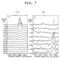
- Fig. 1 shows distribution condition of fluorine and phosphorus on the surface and in the inside of the fluorine passivated film, which is the result detected by an electron spectroscopy for chemical analysis (ESCA).
- Fig. 1(A) is a diagram showing distribution condition of fluorine
- Fig. 1(B) is a diagram showing distribution condition of phosphorus.
- the axis of ordinates shows etching time (minute) from the surface of the fluorine passivated film
- the axis of abscissas shows binding energy proper to a chemical element.
- fluorine (F) is distributed on the surface and in the vicinity of the surface of the fluorine passivated film, but is not distributed in the inside thereof.
- phosphorus (P) is not distributed on the surface and in the vicinity of the fluorine passivated film, but is distributed in gradually greater quantities toward the inside thereof. Incidentally, the boundary between the nickel-phosphorus plating film and the fluorine passivated film is not clearly distinguished.
- Fig. 2 shows the distribution condition of fluorine and boron, detected by the ESCA, on the surface and in the inside of the fluorine passivated film in the case where the nickel-boron alloy film is formed on the substrate instead of the nickel-phosphorus alloy plating film, and then fluoridation is performed. Nickel and oxygen are simultaneously detected in this analysis.
- fluorine (F) is distributed in a great quantities on the surface and in the vicinity of the fluorine passivated film, and distributed in less quantities toward the inside thereof.
- boron (B) is not distributed on the surface and in the vicinity of the fluorine passivated film, but is distributed in greater quantities toward the inside thereof.
- Fig. 3 shows the distribution condition of fluorine, tungsten and phosphorus, detected by the ESCA, on the surface and in the inside of the fluorine passivated film in the case where the nickel-tungsten-phosphorus alloy plating film is formed on the substrate instead of the nickel-phosphorus alloy plating film, and then fluoridation is performed. Nickel and oxygen are simultaneously detected in this analysis as well as Fig. 2.
- fluorine (F) is distributed in a great quantities on the surface and in the vicinity of the fluorine passivated film, and distributed in less quantities toward the inside thereof.
- tungsten (W) and phosphorus (P) is not distributed on the surface and in the vicinity of the fluorine passivated film, but is distributed in greater quantities toward the inside thereof.
- Fig. 4(A) shows the thickness of fluoride in the case where the nickel alloy film containing nickel, semimetal and/or other metal whose fluoride becomes a volatile compound is not formed on the substrate, but only the nickel film is formed, and then metallic fluoride (NiF2) is formed on the surface thereof.
- NiF2 metallic fluoride
- Fig. 4(B) shows the thickness of metallic fluoride in the case where the nickel-phosphorus alloy film containing 8% phosphorus, which is nickel alloy film containing nickel and other metal whose fluoride becomes a volatile compound or semimetal, is formed on the substrate, and then metallic fluoride is formed on the surface thereof.
- the content of fluorine is approximately 29%. This still represents distribution of a sufficient quantity of fluorine in this depth.
- the nickel alloy film containing nickel, semimetal and/or other metal whose fluoride becomes a volatile compound is formed on the substrate, thereby thickening film of the metallic fluoride.
- the substrate used aluminum or aluminum alloy in this example. After the said fluoridation treatment, the substrate was kept in gas atmosphere comprising 5 volume % of HF, 1 volume % of H2O and 94 volume % of N2 for 72 hours, or in Cl2 gas atmosphere of gauge pressure 2kg/cm2 for 7 days, and then the surface of the substrate was observed by an electron microscope. This test result proved that corrosion of the substrate was not observed in both cases, and corrosion resistance to corrosive gas was extremely high.
- the result was evaluated by whether or not change occurs by observing by microscope and the naked eyes.
- metal material such as metal and metal alloy as a substrate are used and explained, however, nonmetal material such as plastics or ceramics may be used, that is, the grounding treatment, formation of film, and fluoridation may be carried out in the same way as mentioned above.
- the industrial material with fluorine passivated film according to the present invention is applicable to gas cylinders, gas holders, pipes, valves, RIE, CVD, excimer laser oscillators or the like.
- the nickel alloy film containing nickel, semimetal and/or other metal except- for nickel whose fluoride becomes a volatile compound is formed on the substrate, the nickel alloy film becomes stable by the presence of said other metal or semimetal.
- the thick fluorine passivated film can be formed by the presence of said other metal or semimetal.
- the fluorine passivated film is applicable to the industrial material in semiconductor manufacturing field without any bad influence.
- corrosion resistance can be improved.
- plastics or ceramics as a substrate, gas released from the surface of the substrate can be prevented and conductivity can also be obtained.
Landscapes
- Chemical & Material Sciences (AREA)
- Engineering & Computer Science (AREA)
- Electromagnetism (AREA)
- Physics & Mathematics (AREA)
- Mechanical Engineering (AREA)
- Optics & Photonics (AREA)
- Chemical Kinetics & Catalysis (AREA)
- Materials Engineering (AREA)
- Plasma & Fusion (AREA)
- Metallurgy (AREA)
- Organic Chemistry (AREA)
- Composite Materials (AREA)
- Inorganic Chemistry (AREA)
- Other Surface Treatments For Metallic Materials (AREA)
- Chemically Coating (AREA)
- Preventing Corrosion Or Incrustation Of Metals (AREA)
- Compounds Of Alkaline-Earth Elements, Aluminum Or Rare-Earth Metals (AREA)
- Glass Compositions (AREA)
Applications Claiming Priority (10)
| Application Number | Priority Date | Filing Date | Title |
|---|---|---|---|
| JP5944390 | 1990-03-08 | ||
| JP59443/90 | 1990-03-09 | ||
| JP177172/90 | 1990-07-04 | ||
| JP17717290 | 1990-07-04 | ||
| JP283151/90 | 1990-10-19 | ||
| JP28315190 | 1990-10-19 | ||
| JP283150/90 | 1990-10-19 | ||
| JP28315090 | 1990-10-19 | ||
| JP40513190 | 1990-12-21 | ||
| JP405131/90 | 1990-12-21 |
Publications (2)
| Publication Number | Publication Date |
|---|---|
| EP0446079A1 EP0446079A1 (en) | 1991-09-11 |
| EP0446079B1 true EP0446079B1 (en) | 1995-07-26 |
Family
ID=27523511
Family Applications (1)
| Application Number | Title | Priority Date | Filing Date |
|---|---|---|---|
| EP91302016A Expired - Lifetime EP0446079B1 (en) | 1990-03-08 | 1991-03-11 | Industrial material with fluorine passivated film and process of manufacturing the same |
Country Status (5)
| Country | Link |
|---|---|
| US (1) | US6258411B1 (ja) |
| EP (1) | EP0446079B1 (ja) |
| JP (1) | JP2954716B2 (ja) |
| AT (1) | ATE125642T1 (ja) |
| DE (1) | DE69111488T2 (ja) |
Cited By (1)
| Publication number | Priority date | Publication date | Assignee | Title |
|---|---|---|---|---|
| US12031213B2 (en) | 2019-07-31 | 2024-07-09 | Resonac Corporation | Laminate |
Families Citing this family (11)
| Publication number | Priority date | Publication date | Assignee | Title |
|---|---|---|---|---|
| JPH0464226A (ja) * | 1990-07-04 | 1992-02-28 | Tadahiro Omi | 金属フッ化膜を備えた電子装置 |
| EP0794598B1 (en) * | 1996-03-07 | 2002-11-20 | Canon Kabushiki Kaisha | Excimer laser generator |
| JP3094000B2 (ja) * | 1997-09-12 | 2000-10-03 | 昭和電工株式会社 | フッ化表面層を有する金属材料もしくは金属皮膜ならびにフッ化方法 |
| US6444083B1 (en) * | 1999-06-30 | 2002-09-03 | Lam Research Corporation | Corrosion resistant component of semiconductor processing equipment and method of manufacturing thereof |
| JP5001489B2 (ja) * | 2001-03-19 | 2012-08-15 | 東京エレクトロン株式会社 | 処理装置 |
| JP3891815B2 (ja) * | 2001-10-12 | 2007-03-14 | 昭和電工株式会社 | 皮膜形成処理用アルミニウム合金、ならびに耐食性に優れたアルミニウム合金材およびその製造方法 |
| CN100392151C (zh) * | 2003-05-09 | 2008-06-04 | 昭和电工株式会社 | 耐腐蚀性材料及其制造方法 |
| US20060228569A1 (en) * | 2003-08-08 | 2006-10-12 | Tadaaki Kojima | Production method of substrate with black film and substrate with black film |
| WO2021049235A1 (ja) | 2019-09-13 | 2021-03-18 | 昭和電工株式会社 | 積層体およびその製造方法 |
| WO2021070561A1 (ja) | 2019-10-10 | 2021-04-15 | 昭和電工株式会社 | 積層体およびその製造方法 |
| KR102448366B1 (ko) | 2020-12-21 | 2022-09-29 | 에스케이스페셜티 주식회사 | 내스크래치성이 향상된 고순도 불화수소의 저장 용기용 금속재료 및 이의 제조 방법 |
Family Cites Families (7)
| Publication number | Priority date | Publication date | Assignee | Title |
|---|---|---|---|---|
| US4397812A (en) * | 1974-05-24 | 1983-08-09 | Richardson Chemical Company | Electroless nickel polyalloys |
| DE2751517C2 (de) * | 1977-11-18 | 1983-10-20 | Licentia Patent-Verwaltungs-Gmbh, 6000 Frankfurt | Oberflächenpassiviertes Halbleiterbauelement mit einer Halbleiterscheibe und Verfahren zur Herstellung desselben |
| JPS5913065A (ja) | 1982-07-13 | 1984-01-23 | Fujitsu Ltd | 薄膜防食法 |
| DE3407093A1 (de) * | 1984-02-28 | 1985-08-29 | Licentia Patent-Verwaltungs-Gmbh, 6000 Frankfurt | Verfahren zur passivierung einer metallischen oberflaeche |
| US4608097A (en) * | 1984-10-05 | 1986-08-26 | Exxon Research And Engineering Co. | Method for producing an electronically passivated surface on crystalline silicon using a fluorination treatment and an organic overlayer |
| US5009963A (en) | 1988-07-20 | 1991-04-23 | Tadahiro Ohmi | Metal material with film passivated by fluorination and apparatus composed of the metal material |
| DE68918365T2 (de) * | 1988-07-20 | 1995-05-04 | Hashimoto Chemical Ind Co | Metallischer Werkstoff mit durch Fluorierung passiviertem Film und aus dem metallischen Werkstoff bestehende Anlage. |
-
1991
- 1991-02-20 JP JP3026214A patent/JP2954716B2/ja not_active Expired - Lifetime
- 1991-03-11 AT AT91302016T patent/ATE125642T1/de not_active IP Right Cessation
- 1991-03-11 EP EP91302016A patent/EP0446079B1/en not_active Expired - Lifetime
- 1991-03-11 DE DE69111488T patent/DE69111488T2/de not_active Expired - Lifetime
-
1999
- 1999-04-27 US US09/300,773 patent/US6258411B1/en not_active Expired - Fee Related
Cited By (1)
| Publication number | Priority date | Publication date | Assignee | Title |
|---|---|---|---|---|
| US12031213B2 (en) | 2019-07-31 | 2024-07-09 | Resonac Corporation | Laminate |
Also Published As
| Publication number | Publication date |
|---|---|
| JPH05302177A (ja) | 1993-11-16 |
| US6258411B1 (en) | 2001-07-10 |
| JP2954716B2 (ja) | 1999-09-27 |
| EP0446079A1 (en) | 1991-09-11 |
| DE69111488D1 (de) | 1995-08-31 |
| ATE125642T1 (de) | 1995-08-15 |
| DE69111488T2 (de) | 1996-01-11 |
Similar Documents
| Publication | Publication Date | Title |
|---|---|---|
| EP0446079B1 (en) | Industrial material with fluorine passivated film and process of manufacturing the same | |
| JP5138637B2 (ja) | 半導体プロセス装置用の耐腐食性アルミニウム物品 | |
| US6280597B1 (en) | Fluorinated metal having a fluorinated layer and process for its production | |
| US5545262A (en) | Method of preparing a metal substrate of improved surface morphology | |
| EP0408168B1 (en) | Method of pretreating metallic works and method of nitriding steel | |
| JP3094000B2 (ja) | フッ化表面層を有する金属材料もしくは金属皮膜ならびにフッ化方法 | |
| US6215806B1 (en) | Excimer laser generator provided with a laser chamber with a fluoride passivated inner surface | |
| WO2003066920A1 (en) | Halogen-resistant, anodized aluminum for use in semiconductor processing apparatus | |
| US6274257B1 (en) | Forming members for shaping a reactive metal and methods for their fabrication | |
| US5167788A (en) | Metal substrate of improved surface morphology | |
| EP1088803B1 (en) | Corrosion-resistant member and method of producing same | |
| US5262040A (en) | Method of using a metal substrate of improved surface morphology | |
| KR100218282B1 (ko) | 불화부동태막을 형성하여된 공업재료 및 그의 제조방법 | |
| JP3955294B2 (ja) | 半導体加工装置用部材の耐食処理方法およびその処理部材 | |
| JP2004360066A (ja) | 耐食性材料およびその製造方法 | |
| EP1179609A1 (en) | A process for nitriding an aluminum-containing substrate | |
| KR102727364B1 (ko) | 적층체 및 그 제조 방법 | |
| CN100392151C (zh) | 耐腐蚀性材料及其制造方法 | |
| JPH09302499A (ja) | アルミニウム材 | |
| JP3020673B2 (ja) | チタン合金素材のめっき前処理法 | |
| JP3115103B2 (ja) | フッ化不働態膜を形成した工業材料 | |
| JP3809879B2 (ja) | アルマイト処理によって形成されたアルミナ膜を有するレーザーチャンバーを備えたエキシマレーザー発振装置 | |
| KR102940228B1 (ko) | 적층체 및 그 제조 방법 | |
| JP2002038252A (ja) | 耐熱性構造体、耐ハロゲン系腐食性ガス材料および耐ハロゲン系腐食性ガス性構造体 | |
| KR950012809B1 (ko) | 불화부동태막이 형성된 금속재료 및 그 금속재료를 사용한 장치 |
Legal Events
| Date | Code | Title | Description |
|---|---|---|---|
| PUAI | Public reference made under article 153(3) epc to a published international application that has entered the european phase |
Free format text: ORIGINAL CODE: 0009012 |
|
| AK | Designated contracting states |
Kind code of ref document: A1 Designated state(s): AT BE CH DE DK ES FR GB GR IT LI LU NL SE |
|
| 17P | Request for examination filed |
Effective date: 19920228 |
|
| 17Q | First examination report despatched |
Effective date: 19940207 |
|
| GRAA | (expected) grant |
Free format text: ORIGINAL CODE: 0009210 |
|
| AK | Designated contracting states |
Kind code of ref document: B1 Designated state(s): AT BE CH DE DK ES FR GB GR IT LI LU NL SE |
|
| PG25 | Lapsed in a contracting state [announced via postgrant information from national office to epo] |
Ref country code: IT Free format text: LAPSE BECAUSE OF FAILURE TO SUBMIT A TRANSLATION OF THE DESCRIPTION OR TO PAY THE FEE WITHIN THE PRE;WARNING: LAPSES OF ITALIAN PATENTS WITH EFFECTIVE DATE BEFORE 2007 MAY HAVE OCCURRED AT ANY TIME BEFORE 2007. THE CORRECT EFFECTIVE DATE MAY BE DIFFERENT FROM THE ONE RECORDED.SCRIBED TIME-LIMIT Effective date: 19950726 Ref country code: LI Effective date: 19950726 Ref country code: GR Free format text: LAPSE BECAUSE OF FAILURE TO SUBMIT A TRANSLATION OF THE DESCRIPTION OR TO PAY THE FEE WITHIN THE PRESCRIBED TIME-LIMIT Effective date: 19950726 Ref country code: ES Free format text: THE PATENT HAS BEEN ANNULLED BY A DECISION OF A NATIONAL AUTHORITY Effective date: 19950726 Ref country code: CH Effective date: 19950726 Ref country code: BE Effective date: 19950726 Ref country code: AT Effective date: 19950726 Ref country code: DK Effective date: 19950726 Ref country code: NL Free format text: LAPSE BECAUSE OF FAILURE TO SUBMIT A TRANSLATION OF THE DESCRIPTION OR TO PAY THE FEE WITHIN THE PRESCRIBED TIME-LIMIT Effective date: 19950726 |
|
| REF | Corresponds to: |
Ref document number: 125642 Country of ref document: AT Date of ref document: 19950815 Kind code of ref document: T |
|
| REF | Corresponds to: |
Ref document number: 69111488 Country of ref document: DE Date of ref document: 19950831 |
|
| PG25 | Lapsed in a contracting state [announced via postgrant information from national office to epo] |
Ref country code: SE Effective date: 19951026 |
|
| ET | Fr: translation filed | ||
| NLV1 | Nl: lapsed or annulled due to failure to fulfill the requirements of art. 29p and 29m of the patents act | ||
| PG25 | Lapsed in a contracting state [announced via postgrant information from national office to epo] |
Ref country code: LU Free format text: LAPSE BECAUSE OF NON-PAYMENT OF DUE FEES Effective date: 19960331 |
|
| PLBE | No opposition filed within time limit |
Free format text: ORIGINAL CODE: 0009261 |
|
| STAA | Information on the status of an ep patent application or granted ep patent |
Free format text: STATUS: NO OPPOSITION FILED WITHIN TIME LIMIT |
|
| 26N | No opposition filed | ||
| REG | Reference to a national code |
Ref country code: GB Ref legal event code: IF02 |
|
| PGFP | Annual fee paid to national office [announced via postgrant information from national office to epo] |
Ref country code: FR Payment date: 20100324 Year of fee payment: 20 |
|
| PGFP | Annual fee paid to national office [announced via postgrant information from national office to epo] |
Ref country code: GB Payment date: 20100310 Year of fee payment: 20 |
|
| PGFP | Annual fee paid to national office [announced via postgrant information from national office to epo] |
Ref country code: DE Payment date: 20100318 Year of fee payment: 20 |
|
| REG | Reference to a national code |
Ref country code: DE Ref legal event code: R071 Ref document number: 69111488 Country of ref document: DE |
|
| REG | Reference to a national code |
Ref country code: GB Ref legal event code: PE20 Expiry date: 20110310 |
|
| PG25 | Lapsed in a contracting state [announced via postgrant information from national office to epo] |
Ref country code: GB Free format text: LAPSE BECAUSE OF EXPIRATION OF PROTECTION Effective date: 20110310 |
|
| PG25 | Lapsed in a contracting state [announced via postgrant information from national office to epo] |
Ref country code: DE Free format text: LAPSE BECAUSE OF EXPIRATION OF PROTECTION Effective date: 20110311 |