EP0449000A2 - Schichtstruktur mit Kontaktierungsöffnung für flossenförmige Kondensatoren in DRAMS und Methode zur Herstellung desselben - Google Patents
Schichtstruktur mit Kontaktierungsöffnung für flossenförmige Kondensatoren in DRAMS und Methode zur Herstellung desselben Download PDFInfo
- Publication number
- EP0449000A2 EP0449000A2 EP91103412A EP91103412A EP0449000A2 EP 0449000 A2 EP0449000 A2 EP 0449000A2 EP 91103412 A EP91103412 A EP 91103412A EP 91103412 A EP91103412 A EP 91103412A EP 0449000 A2 EP0449000 A2 EP 0449000A2
- Authority
- EP
- European Patent Office
- Prior art keywords
- layer
- insulating layer
- conductive
- conductive layer
- contact hole
- Prior art date
- Legal status (The legal status is an assumption and is not a legal conclusion. Google has not performed a legal analysis and makes no representation as to the accuracy of the status listed.)
- Granted
Links
Images











Classifications
-
- H—ELECTRICITY
- H10—SEMICONDUCTOR DEVICES; ELECTRIC SOLID-STATE DEVICES NOT OTHERWISE PROVIDED FOR
- H10W—GENERIC PACKAGES, INTERCONNECTIONS, CONNECTORS OR OTHER CONSTRUCTIONAL DETAILS OF DEVICES COVERED BY CLASS H10
- H10W20/00—Interconnections in chips, wafers or substrates
- H10W20/01—Manufacture or treatment
- H10W20/071—Manufacture or treatment of dielectric parts thereof
- H10W20/081—Manufacture or treatment of dielectric parts thereof by forming openings in the dielectric parts
-
- H—ELECTRICITY
- H10—SEMICONDUCTOR DEVICES; ELECTRIC SOLID-STATE DEVICES NOT OTHERWISE PROVIDED FOR
- H10B—ELECTRONIC MEMORY DEVICES
- H10B12/00—Dynamic random access memory [DRAM] devices
- H10B12/01—Manufacture or treatment
- H10B12/02—Manufacture or treatment for one transistor one-capacitor [1T-1C] memory cells
- H10B12/03—Making the capacitor or connections thereto
- H10B12/033—Making the capacitor or connections thereto the capacitor extending over the transistor
-
- H—ELECTRICITY
- H10—SEMICONDUCTOR DEVICES; ELECTRIC SOLID-STATE DEVICES NOT OTHERWISE PROVIDED FOR
- H10B—ELECTRONIC MEMORY DEVICES
- H10B12/00—Dynamic random access memory [DRAM] devices
- H10B12/30—DRAM devices comprising one-transistor - one-capacitor [1T-1C] memory cells
- H10B12/31—DRAM devices comprising one-transistor - one-capacitor [1T-1C] memory cells having a storage electrode stacked over the transistor
- H10B12/318—DRAM devices comprising one-transistor - one-capacitor [1T-1C] memory cells having a storage electrode stacked over the transistor the storage electrode having multiple segments
-
- H—ELECTRICITY
- H10—SEMICONDUCTOR DEVICES; ELECTRIC SOLID-STATE DEVICES NOT OTHERWISE PROVIDED FOR
- H10B—ELECTRONIC MEMORY DEVICES
- H10B12/00—Dynamic random access memory [DRAM] devices
- H10B12/30—DRAM devices comprising one-transistor - one-capacitor [1T-1C] memory cells
- H10B12/48—Data lines or contacts therefor
- H10B12/488—Word lines
-
- H—ELECTRICITY
- H10—SEMICONDUCTOR DEVICES; ELECTRIC SOLID-STATE DEVICES NOT OTHERWISE PROVIDED FOR
- H10P—GENERIC PROCESSES OR APPARATUS FOR THE MANUFACTURE OR TREATMENT OF DEVICES COVERED BY CLASS H10
- H10P76/00—Manufacture or treatment of masks on semiconductor bodies, e.g. by lithography or photolithography
- H10P76/40—Manufacture or treatment of masks on semiconductor bodies, e.g. by lithography or photolithography of masks comprising inorganic materials
- H10P76/405—Manufacture or treatment of masks on semiconductor bodies, e.g. by lithography or photolithography of masks comprising inorganic materials characterised by their composition, e.g. multilayer masks
-
- H—ELECTRICITY
- H10—SEMICONDUCTOR DEVICES; ELECTRIC SOLID-STATE DEVICES NOT OTHERWISE PROVIDED FOR
- H10P—GENERIC PROCESSES OR APPARATUS FOR THE MANUFACTURE OR TREATMENT OF DEVICES COVERED BY CLASS H10
- H10P76/00—Manufacture or treatment of masks on semiconductor bodies, e.g. by lithography or photolithography
- H10P76/40—Manufacture or treatment of masks on semiconductor bodies, e.g. by lithography or photolithography of masks comprising inorganic materials
- H10P76/408—Manufacture or treatment of masks on semiconductor bodies, e.g. by lithography or photolithography of masks comprising inorganic materials characterised by their sizes, orientations, dispositions, behaviours or shapes
- H10P76/4085—Manufacture or treatment of masks on semiconductor bodies, e.g. by lithography or photolithography of masks comprising inorganic materials characterised by their sizes, orientations, dispositions, behaviours or shapes characterised by the processes involved to create the masks
-
- H—ELECTRICITY
- H10—SEMICONDUCTOR DEVICES; ELECTRIC SOLID-STATE DEVICES NOT OTHERWISE PROVIDED FOR
- H10W—GENERIC PACKAGES, INTERCONNECTIONS, CONNECTORS OR OTHER CONSTRUCTIONAL DETAILS OF DEVICES COVERED BY CLASS H10
- H10W20/00—Interconnections in chips, wafers or substrates
- H10W20/01—Manufacture or treatment
- H10W20/031—Manufacture or treatment of conductive parts of the interconnections
- H10W20/032—Manufacture or treatment of conductive parts of the interconnections of conductive barrier, adhesion or liner layers
- H10W20/033—Manufacture or treatment of conductive parts of the interconnections of conductive barrier, adhesion or liner layers in openings in dielectrics
-
- H—ELECTRICITY
- H10—SEMICONDUCTOR DEVICES; ELECTRIC SOLID-STATE DEVICES NOT OTHERWISE PROVIDED FOR
- H10W—GENERIC PACKAGES, INTERCONNECTIONS, CONNECTORS OR OTHER CONSTRUCTIONAL DETAILS OF DEVICES COVERED BY CLASS H10
- H10W20/00—Interconnections in chips, wafers or substrates
- H10W20/01—Manufacture or treatment
- H10W20/031—Manufacture or treatment of conductive parts of the interconnections
- H10W20/032—Manufacture or treatment of conductive parts of the interconnections of conductive barrier, adhesion or liner layers
- H10W20/046—Manufacture or treatment of conductive parts of the interconnections of conductive barrier, adhesion or liner layers the barrier, adhesion or liner layers being associated with interconnections of capacitors
-
- H—ELECTRICITY
- H10—SEMICONDUCTOR DEVICES; ELECTRIC SOLID-STATE DEVICES NOT OTHERWISE PROVIDED FOR
- H10P—GENERIC PROCESSES OR APPARATUS FOR THE MANUFACTURE OR TREATMENT OF DEVICES COVERED BY CLASS H10
- H10P14/00—Formation of materials, e.g. in the shape of layers or pillars
- H10P14/60—Formation of materials, e.g. in the shape of layers or pillars of insulating materials
- H10P14/69—Inorganic materials
- H10P14/692—Inorganic materials composed of oxides, glassy oxides or oxide-based glasses
- H10P14/6921—Inorganic materials composed of oxides, glassy oxides or oxide-based glasses containing silicon
- H10P14/6922—Inorganic materials composed of oxides, glassy oxides or oxide-based glasses containing silicon the material containing Si, O and at least one of H, N, C, F or other non-metal elements, e.g. SiOC, SiOC:H or SiONC
- H10P14/6923—Inorganic materials composed of oxides, glassy oxides or oxide-based glasses containing silicon the material containing Si, O and at least one of H, N, C, F or other non-metal elements, e.g. SiOC, SiOC:H or SiONC the material being boron or phosphorus doped silicon oxides, e.g. BPSG, BSG or PSG
-
- Y—GENERAL TAGGING OF NEW TECHNOLOGICAL DEVELOPMENTS; GENERAL TAGGING OF CROSS-SECTIONAL TECHNOLOGIES SPANNING OVER SEVERAL SECTIONS OF THE IPC; TECHNICAL SUBJECTS COVERED BY FORMER USPC CROSS-REFERENCE ART COLLECTIONS [XRACs] AND DIGESTS
- Y10—TECHNICAL SUBJECTS COVERED BY FORMER USPC
- Y10S—TECHNICAL SUBJECTS COVERED BY FORMER USPC CROSS-REFERENCE ART COLLECTIONS [XRACs] AND DIGESTS
- Y10S148/00—Metal treatment
- Y10S148/014—Capacitor
Definitions
- the present invention generally relates to a layer structure having a contact hole suitable for dynamic random access memories having fine contact holes, and a method of producing such a layer structure. More particularly, the present invention is concerned with a fin-shaped capacitor having such a layer structure, and a method of forming such a fin-shaped capacitor. Furthermore, the present invention is concerned with a dynamic random access memory having such a fin-shaped capacitor.
- DRAM dynamic random access memories
- it is necessary to reduce the two-dimensional size of each memory cell without reducing the capacitance of each stacked capacitor.
- 64Mbit DRAMs In order to fabricate 64Mbit DRAMs, a feature scale approximately equal to 0.3 [ ⁇ m] is required. However, the conventional photolithography technique can realize a feature scale approximately equal to a maximum of 0.5 [ ⁇ m]. 64Mbit DRAMs can be realized by reducing the size of each storage (stacked) capacitor. For this purpose, it is necessary to reduce the size of a contact window (opening) for a storage electrode which is a part of the stacked capacitor. As described above, since the feature scale realized by the conventional photolithography technique is approximately 0.5 [ ⁇ m], it is impossible to form the contact window having a size approximately equal to 0.3 [ ⁇ m].
- a window provided for connecting a word line formed of, for example, polysilicon, and a low-resistance wiring line (word-line shunt layer) formed of Al or Al alloy, directed to preventing the occurrence of a delay in signal transmission in the word line.
- Japanese Laid-Open Patent Application No. 63-119239 discloses a method for forming a fine pattern narrower than a feature scale limit of the conventional photolithography technique.
- the application teaches a process in which polysilicon, PSG or SiO2 is grown on an SiO2 mask having a window through which a substrate is partially exposed, and a grown film on the mask and the exposed substrate surface is anisotropically etched, so that a sidewall is formed on the substrate so that it is formed around the entire inner wall of the window in the mask.
- the distance between opposite surfaces of the sidewall in the window is less than the feature scale limit.
- a surface area of the substrate less than the feature scale limit is exposed through the sidewall in the window.
- the substrate is etched in such a way that the combination of the sidewall and the mask function as an etching mask, so that a hole is formed in the substrate.
- the above-mentioned Patent Application discloses an arrangement in which the mask is formed of SiO2 and a member to be processed is formed of Si. Thus, the removal of the mask material can be easily made.
- a multilayer structure such as DRAMS
- the above-mentioned Japanese Application does not suggest the above matters.
- Japanese Laid-Open Patent Application No. 60-224218 discloses the use of a sidewall directed to providing a window (contact hole) smaller than the feature scale limit of the conventional photolithography technique.
- the sidewall is formed of Al and formed on an SiO2 layer and around an inner wall of a window formed in a silicon nitride (Si3N4) layer also formed on the SiO2 layer.
- the SiO2 layer is selectively etched in such a way that the Al sidewall and the Si3N4 layer function as mask layers.
- it is very difficult to form the Al sidewall in contact with the inner wall of the window in the Si3N4 layer since Al has a poor coverage characteristic.
- Japanese Laid-Open Patent Application No. 63-116430 (which corresponds to U.S. patent application S.N. 924,223 filed on October 28, 1986) teaches the use of a sidewall for forming a hole smaller than the scale limit of the conventional photolithgraphy technique.
- the just above application shows a lift-off process for removing the mask material.
- the lift-off process has a problem in that some of the mask material separated from the substrate is re-adhered hereto. This frequently causes a pattern fault in a subsequent process.
- the Japanese application of concern does not disclose an effective step to process the mask material.
- the Japanese application shows a sidewall formed on the side surface of a photosensitive material. It is necessary to form the sidewall at a low temperature due to the thermal stability of the photosensitive material. Thus, there is a great limitation regarding the selection of mask materials.
- the structure shown in the Japanese application of concern is limited to a special application.
- a more specific object of the present invention is to provide a layer structure having a contact hole suitable for DRAMs.
- Another object of the present invention is to provide a layer structure having a contact hole as formed by the above-mentioned methods.
- a layer structure comprising: a first conductive layer; an insulating layer formed on the first conductive layer and having a contact hole, the first conductive layer being exposed through the contact hole; a second conductive layer formed on the insulating layer and having an opening having a width larger than that of the contact hole; a conductive sidewall formed on the insulating layer exposed through the opening and formed around an inner wall of the second conductive layer defining the opening, the conductive sidewall having a width substantially equal to that of the contact hole; a barrier layer formed on the second conductive layer, the conductive sidewall and the first conductive layer exposed through the contact hole; and a third conductive layer formed on the barrier layer, the barrier layer preventing the third conductive layer from reacting with the second conductive layer and the conductive sidewall.
- a layer structure comprising: a first conductive layer; an insulating layer formed on the first conductive layer and having a contact hole, the first conductive layer being exposed through the contact hole; a second conductive layer formed on the insulating layer and having a first opening having a width larger than that of the contact hole; a third conductive layer formed on the insulating layer exposed through the first opening and the second conductive layer and formed around an inner wall of the second conductive layer defining the first opening, the third conductive layer defining a second opening having a width substantially equal to that of the contact hole, the second opening being continuously connected to the contact hole; a barrier layer formed on the third conductive layer and the first conductive layer exposed through the contact hole; and a fourth conductive layer formed on the barrier layer, the barrier layer preventing the fourth conductive layer from reacting with the third conductive layer and the conductive sidewall.
- a layer structure comprising: a first conductive layer; an insulating layer formed on the first conductive layer and having a contact hole, the first conductive layer being exposed through the contact hole; a second conductive layer formed on the insulating layer and having an opening having a width larger than that of the contact hole; a conductive sidewall formed on the insulating layer exposed through the opening and formed around an inner wall of the second conductive layer defining the opening, the conductive sidewall having a width substantially equal to that of the contact hole; and a third conductive layer formed on the second conductive layer, the conductive sidewall and the first conductive layer exposed through the contact hole, wherein the third conductive layer comprises a material which causes no reaction with the second conductive layer and the conductive sidewall.
- a fin-shaped capacitor and a method for producing such a fin-shaped capacitor.
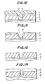
- a conductive layer 2 formed of, for example, polysilicon is formed on a base 1 formed of an insulator, such as SiO2.
- the polysilicon layer 2 is a word line of a DRAM, for example.
- the BPSG layer 3 is heated in a wet atmosphere at 850°C for 10 minutes, and reflown, so that a substantially flat surface of the BPSG layer 3 can be formed.
- a polysilicon layer 4 is grown to, for example, 1000 angstrom by the CVD process.
- a photoresist film 5 is coated, and etched by the conventional photolithography technique, so that the photoresist film 5 functions as an etching resist having a hole pattern can be formed.
- the polysilicon layer 4 is selectively etched by an RIE (reactive ion etching) process in which a CCl4/O2 gas is used and the photoresist film 5 functions as an etching mask.
- RIE reactive ion etching
- a polysilicon layer 7 is grown to, for example, 1500 angstroms on the entire surface including the first opening 6 by CVD. Then, as shown in FIG.1C, the polysilicon layer 7 is selectively etched by the RIE process using a CCl4/O2 gas, so that a sidewall 8 is formed on an inner wall (sidewall) of the first opening 6 formed in the polysilicon layer 4.
- the sidewall 8 defines a second opening 9 having a width approximately equal to 0.2 ⁇ m.
- the BPSG layer 3 is selectively etched in an RIE process using a CHF3/He gas in which the polysilicon layer 4 and the sidewall 8 function as masks. Thereby, a contact hole 10 through which the polysilicon layer 2 is partially exposed is formed in the BPSG layer 3.
- a photoresist film 11 is formed on the entire surface including the contact hole 10. Then, as shown in FIG.1F, the entire surface of the photoresist film 11 is exposed and developed. During this process, a small amount of light enters a bottom portion of the contact hole 10. Thus, a part of the photoresist film 11 is left in the contact hole 10.
- the polysilicon layer 4 and the sidewall 18 are dry-etched in a CF4/O2 plasma atmosphere in a state where the polysilicon layer 2 is protected against dry etching due to the existence of the photoresist film 11 in the contact hole 10. During the dry etching process, the polysilicon layer 4 and the sidewall 8 are isotropically etched. After that, the photoresist film 11 is removed in an O2 plasma.
- an Al alloy (or Al) 12 is deposited on the upper surface including the contact hole 10 by a sputtering process. Then, the Al alloy layer 12 is etched, so that a desired Al (or Al alloy) pattern is formed. Thereby, the polysilicon word line 2 is connected to the Al alloy layer 12 via the contact hole 10.
- the contact hole 10 has a width smaller than the feature scale limit of the conventional photolithographic technique. It will also be noted that the above-mentioned production method is suitable for forming a contact hole for connecting the word line and the word-line shunt layer which is provided for preventing the occurrence of a delay in transmitting a signal via the word line.
- the BPSG layer 3 can be substituted for a stacked member in which a PSG layer and an SiO2 layer are alternately stacked. It is also possible to employ an alternative step instead of the step shown in FIG.1H. In the alternative step, after the polysilicon layer 4 and the sidewall 8 are removed, the BPSG layer 3 is reflowed by heating the device in an N2 atmosphere at 850°C for 20 minutes, so that an upper edge of the contact hole 10 is smoothly curved. The existence of such a smoothly curved upper edge of the contact hole 10 improves the coverage of the Al alloy layer 12.
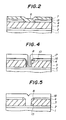
- FIG.2 A layer structure shown in FIG.2 is the same as that shown in FIG.1B except that an SiO2 layer 13 is formed on the polysilicon layer 4. More specifically, the SiO2 film 13 is grown to, for example, about 200 angstroms on the polysilicon layer 4 by CVD. Then, the photoresist film 5 shown in FIG.1A is formed on the entire surface. After that, the first opening 6 is formed in the SiO2 layer 13 and the polysilicon layer 4. Then, the polysilicon layer 7 is formed on the photoresist film 5 and in the first opening 6 in the same way as shown in FIG.1B.
- the polysilicon layer 7 is anisotropically etched in the vertical direction.
- the SiO2 layer 13 functions as an etching stopper during the step shown in FIG.1C, so that it is possible to prevent a decrease in the thickness of the polysilicon layer 4. Further, it becomes easy to detect the end of etching since the SiO2 layer 13 is exposed. It will be noted that the SiO2 layer 13 is removed together with the BPSG layer 3 during the step shown in FIG.1E. Thus, it is not necessary to provide a special step to remove the SiO2 layer 13.
- FIGS.3A through 3C A description will now be given of a third preferred embodiment of the present invention with reference to FIGS.3A through 3C, in which those parts which are the same as those shown in the previous figures are given the same reference numerals.
- the BPSG layer 3 is grown to, for example, 0.5 ⁇ m on the entire surface including the polysilicon layer (word line) 2 by CVD.
- the polysilicon layer 4 is grown to, for example, 1000 angstroms by CVD.
- the photoresist film 5 is coated, and patterned by the conventional photolithography technique, so that a hole pattern having a width approximately equal to 0.5 ⁇ m is formed in the photoresist film 5.
- the polysilicon layer 4 is selectively removed by an RIE process using a CCl4/O2 gas in which the photoresist film 5 serves as a mask, so that the first opening 6 is formed in the polysilicon layer 4.
- a polysilicon layer 14 is selectively grown on the upper surface of the polysilicon layer 4 and a side surface thereof by a CVD process in which the device is maintained at 650°C and an SiH4+HCl+H2 gas is used.
- the polysilicon layer 14 defines a second opening 15 having a width smaller than that of the first opening 6. It is easy to control the thickness of the polysilicon layer 14, that is, easy to control the width of the second opening 15.
- the BPSG layer 3 is removed via the second opening 15 by an RIE process using a CHF3/He gas, so that the contact hole 10 is formed and the polysilicon layer 2 is partially exposed through the contact hole 10.
- a stakced layer 16 fomed of a Ti/TiN layer 16 is formed on the polysilicon layer 14, and an Al alloy (or Al) layer 17 is formed on the stacked layer 16, as shown in FIG.3D.
- the stacked laye 16 will be described in detail later.
- FIG.1G A description will now be given of a fourth preferred embodiment of the present invention with reference to FIG.4, in which those parts which are the same as those shown in the previous figures are given the same reference numerals.
- the polysilicon layer 4 and the sidewall 8 are removed.
- the polysilicon layer 4 and the sidewall 8 are not removed, but left on the BPSG layer 3.
- the stacked layer 16 is formed on the entire surface including the polysilicon layer 4, the sidewall 8 and the exposed surface of the polysilicon layer 2 by CVD, for example.
- the stacked layer 16 consists of a Ti layer having a thickness of 200 angstroms and a TiN layer having a thickness of 1000 angstroms.
- the stacked layer 16 is referred to as a Ti/TiN layer 16.
- the Al alloy (or pure Al) 17 is deposited on the Ti/TiN layer 16 by sputtering.
- the polysilicon layer 4, the Ti/TiN layer 16 and the Al alloy layer 17 are patterned by etching.
- the Al alloy layer (or pure Al layer) 17 is deposited directly on the polysilicon layer 4 and the polysilicon sidewall 8, it will easily react to silicon in the layer 4 and the sidewall 8 during a subsequent annealing process in which a protection cover is formed, for example.
- the above reaction increases the resistance of the Al alloy layer 17.
- the Ti/TiN layer 16 functions as a barrier layer which prevents the above-mentioned reaction.
- the barrier layer 16 is not limited to the Ti/TiN layer.
- the fifth embodiment shown in FIG.5 has the left polysilicon layer 4 and the polysilicon sidewall 8, and uses a W (tungsten) layer functioning as a wiring line instead of the Al alloy (or pure Al) layer 17 shown in FIG.4.
- the use of the W layer 18 does not need the deposition of the Ti/TiN layer 16.
- the W layer 18 is grown to, for example, 5000 angstroms on the entire surface including the polysilicon layer 4, the polysilicon sidewall 8 and the exposed surface of the polysilicon layer 2 by CVD.
- the contact hole 10 is filled with tungsten, so that the coverage of the W layer 18 can be improved. It will be noted that it is easy to fill the contact hole 10 with tungsten by CVD. It will be noted that tungsten has a poor adhession to BPSG or SiO2. On the other hand, as shown in FIG.5, the W layer 18 is formed on the polysilicon layer 4 and the polysilicon sidewall 18. Thus, the adhession problem can be solved.
- the sixth preferred embodiment of the present invention provides a DRAM having a contact hole defined by a sidewall.
- an interlayer isolation insulating layer 22 is grown to, for example, 4000 angstroms on a p-type silicon substrate 21 by a selective thermal oxidation process (a local-oxidation-of-silicon process: LOCOS), in which a silicon nitride layer is used as an oxidation-resistant mask.
- LOCOS local-oxidation-of-silicon process
- a silicon nitride layer serving as the oxidation-resistant mask is removed, so that active areas in the p-type silicon substrate 21 are exposed.
- a gate insulating layer 23 having a thickness equal to, for example, 100 angstroms is formed on the exposed surfaces of the p-type silicon substrate 21 by a thermal oxidation process.
- a polysilicon layer is grown to, for example, 1000 angstroms by CVD.
- the polysilicon layer is patterned by a resist process and RIE process in the photolithography technique in which a CCl4/O2 gas is used.
- word lines WL are formed.
- As ions are introduced into the p-type silicon substrate 21 by an ion implantation process in which the word lines WL and the interlayer isolation insulating layer 2 function as masks.
- an n+-type source region 24 and an N+-type drain region 25 of a transfer transistor of a memory cell are formed in the p-type silicon substrate 21.
- the dose of As ions is equal to, for example, 1 x 10¹⁵ atoms/cm2.
- the source and drain regions 24 and 25 are heated.
- an insulating layer 26 formed of SiO2 is grown to, for example, 1000 angstroms by CVD.
- the SiO2 insulating film 26 is selectively etched in an RIE process in which a CHF3/H2 gas is used, so that a bit line contact hole 24A is formed in the SiO2 insulating film 26. It will be noted that if a positional error occurs in the bit line contact window 24A and thus the word line WL is partially exposed, an exposed portion of the word line WL can be compensated for, as will be described later. Thus, it is sufficient to provide an alignment margin approximately equal to 0.1 ⁇ m when the bit line contact window 24A is approximately 0.5 ⁇ m in diameter. As will be indicated later, it is preferable to remove a portion of the SiO2 insulating layer 26 in a scribe area defined in a peripheral portion of a chip at the same time as then the bit line contact hole 24A is formed.
- an SiO2 insulating layer 41 is grown to, for example, 1000 angstroms on the entire surface by CVD.
- the SiO2 insulating layer 41 is selectively etched by an anisotropic etching process, such as, an RIE process using a CHF3/H2 gas.
- an anisotropic etching process such as, an RIE process using a CHF3/H2 gas.
- RIE process a sidewall SW1 having an about 0.1 ⁇ m thickness is formed so that it surrounds a vertical inner wall of the bit line contact window 24A and a curved part of the SiO2 insulating layer 26.
- the sidewall SW1 defines the width of the bit line contact hole 24A, which is approximately equal to 0.3 ⁇ m. It will be noted that this dimension, 0.3 ⁇ m, is considerably smaller than the scale limit by the conventional photolithography technique (approximately 0.5 ⁇ m).
- the formation of the sidewall SW1 contributes to reducing the alignment margin. Even if the word line WL is partially exposed due to the positional error of the bit line contact window 24A, the sidewall 24 will completely cover the exposed surface of the
- the above-mentioned contact hole forming process is distinguished from a known self-alignment contact formation method.
- the self-alignment contact formation method an insulating layer corresponding to the SiO2 insulating layer 26 and a polysilicon layer provided for the word lines WL are patterned into an identical shape. Then, sidewalls are formed around windows. Thus, the windows are automatically defined by the sidewalls, so that there is no need for any alignment margin.
- the insulating film corresponding to the SiO2 insulating layer 26 is 2000 angstroms thick
- the underlying polysilicon layer provided for forming the word lines WL is 1000 angstroms thick.
- the sidewall is about 3000 angstrom high, and is a large step portion formed on the surface of the substrate.
- the process which has been described with reference to FIG.6D does not form such a great step surface portion.
- the sidewall SW1 is also formed on a step portion on the surface of the SiO2 insulating film, so that the slope of the curved surface portion of the SiO2 insulating layer 26 can be reduced.
- the SiO2 insulating layer 41 It is necessary to etch only the SiO2 insulating layer 41. As has been described previously, the scribe area on the peripheral portion of the chip is exposed during the process shown in FIG.6B. Since the SiO2 layer 41 is formed on the scribe area, etching is stopped when the scribe area which is a part of the p-type silicon substrate 21 appears. This judgment of whether or not the scribe area has appeared can be carried out by detecting a change of a plasma emitting state during the RIE process, or by detecting the film thickness of the scribe area by means of a laser interference instrument.
- a polysilicon layer is grown to, for example, 500 angstroms on the entire surface by CVD.
- As ions are introduced into the polysilicon layer by an ion implantation process in which the dose of As ions is equal to 1 x 10¹⁵ atoms/cm2.
- a WSi2 film is formed to, for example, 500 angstroms on the impurity doped polysilicon layer by CVD.
- the WSi2 layer and the impurity doped polysilicon layer are patterned by an RIE process using a CCl4/O2 gas, so that a bit line BL having a two-layer structure is formed.
- an insulating layer 27 formed of Si3N4, a spacer layer 28 formed of SiO2 and a polysilicon layer 29' which forms a part of a storage electrode (fin electrode) of a stacked capacitor are grown in this order by CVD.
- the Si3N4 insulating layer 27, the SiO2 spacer layer 28 and the polysilicon layer 29' are, for example, 1000, 500 and 1000 angstroms, respectively. It will be noted that the polysilicon layer 29' plays the important role, as will be described later.
- the polysilicon layer 29' is selectively etched by the resist process and RIE process using a CCl4/O2 gas in the conventional photolithography technique, so that an opening 29A having the same pattern as the storage electrode contact window is formed in the polysilicon layer 29'.
- the opening 29A has a width approximately equal to 0.5 ⁇ m, which is the scale limit attained by the conventional photolithography technique.
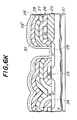
- a polysilicon layer 32a is grown to, for example, 1000 angstroms by CVD. Then, as shown in FIG.6I, the polysilicon layer is anisotropically etched by an RIE process using a CCl4/O2 gas. Thereby, a sidewall 32 formed of polysilicon around the inner surface of the opening 29A in the polysilicon layer is left on the SiO2 spacer layer 28. The sidewall 32 is approximately 0.1 ⁇ m thick. As a result, the opening 29A is reshaped into an opening 32A having a width of about 0.3 ⁇ m. This dimension of the reshaped opening 29A is smaller than the scale limit by the conventional photolithography technique.
- the polysilicon layer 29' and the polysilicon sidewall 32 function as masks when the underlying insulating layers are etched to form the storage electrode contact window. It should be noted that there is no special limitation on the formation of the polysilicon layer 29' and the polysilicon sidewall 32, since they are formed of polysilicon. It should also be noted that the polysilicon layer 29' and the polysilicon sidewall 32 are not removed during a subsequent process, and are utilized as parts of the storage electrode of the stacked capacitor, as will be described in detail later.
- the SiO2 spacer layer 28, the Si3N4 insulating layer 27, the SiO2 insulating layer 26 and the SiO2 gate insulating layer 23 are selectively etched by an RIE process in which a CHF3/H2 is used and the polysilicon layer 29' and the polysilicon sidewall 32 function as the etching masks.
- RIE process a storage electrode contact hole 25A is formed in the above-mentioned layers, so that the n+-type drain region 25 is partially exposed.
- a polysilicon layer 29'' is grown to, for example, 500 angstroms by CVD.
- a part of the polysilicon layer 29'' completely covers the inner wall of the storage electrode contact window 25A and the exposed surface of the n+-type drain region 25. It is important to form the polysilicon layer 29'' in total contact with the Si3N4 insulating layer 27.
- As ions are introduced into the polysilicon layers 29'' and 29' by an ion implantation process in which the dose of the As ions is equal to, for example, 8 x 10¹⁵ atoms/cm2.
- each of the polysilicon layers 29'' and 29' has a reduced resistance. It will be noted toat the layers consisting of the polysilicon layers 29' and 29'' and the sidewall 32 is thicker than the vertically extending portion of the polysilicon layer 29''.
- a spacer layer 33 formed of SiO2 is grown to, for example, 500 angstroms on the entire surface by CVD.
- the SiO2 spacer layer 33 is selectively etched by the resist process and RIE process using a CHF3/H2 gas in the conventional photolithography technique.
- RIE process an opening 33A having a belt shape is formed in the SiO2 spacer layer 33. It is sufficient to form the opening 33A so that it is wider than the storage electrode contact window 25A, because the opening 33A is used for stacking a polysilicon layer (fin) on the integrated polysilicon layer consisting of the layers 29'' and 29' and the polisilicon sidewall 32.
- a polysilicon layer is grown to, for example, 1000 angstroms by CVD.
- As ions are introduced into the polysilicon layer by an ion implantation process in which the dose of As ions is equal to, for example, 1 x 10¹⁵ atoms/cm2. Thereby, the resistance of the polysilicon layer is reduced.
- the above polysilicon layer, the SiO2 spacer layer 33, and the polysilicon layers 29'' and 29' are patterned into an electrode shape by the photoresist process and RIE process using a gas of CCl4+O2 or CHF3+H2.
- the SiO2 spacer layer 33 and the SiO2 spacer layer 28 are completely removed by an etching process in which the device is placed in an HF etchant.
- polysilicon fins 292 and 291 forming a storage electrode 25 of the stacked capacitor are formed.
- the fin 292 has a bottom contact area wider than the contact hole 25A shown in FIG.6J.
- the wall of the Si3N4 insulating layer 27 which is a part of the storage electrode contact window 25A completely makes contact with the polysilicon layer 29', so that there is no possibility that the SiO2 insulating layer 26 and the SiO2 interlayer isolation insulating layer 22 are damaged.
- FIG.6N a dielectric film 36 around an exposed surface of the storage electrode 29 is formed, and a cell plate 37 (opposed electrode) is formed so that it covers the entire surface.
- the dielectric film 36 is formed of, for example, Si3N4.
- the stacked capacitor is made up of the storage electrode 29, the dielectric film 36 and the cell plate 37.
- a PSG layer 38 is formed on the entire surface, and word-line shunt layers 39 formed of, for example, an Al alloy, are formed on the PSG layer 38.
- FIG.7 is a plan view of the DRAM fabricated by the above-mentioned production process. In FIG.7, WL1 and WL2 indicate word lines, and BL1 and BL2 indicate bit lines.
- the word-line shunt layers 39 are connected to the corresponding word lines WL via contact holes (not shown for the sake of simplicity). It is preferable to form such contact holes by the aforementioned first through fifth embodiments of the present invention.
- the lowermost polysilicon fin 291 has the sidewall 32, and the polysilicon layers 29' and 29''.
- the polysilicon layer 29'' is thicker than the polysilicon layer 29', and the largest thickness of the sidewall 32 is approximately equal to the thickness of the polysilicon layer 29'.
- FIGS.8A through 8E A description will now be given of an eighth embodiment of the present invention with reference to FIGS.8A through 8E, in which those parts which are the same as those shown in the previous figures are given the same reference numerals.
- the eighth embodiment of the present invention utilizes the steps which have been described with reference to FIGS.6A through 6L. After the step related to FIG.6L, a step shown in FIG.8A is carried out. A polysilicon layer is grown to, for example, 1000 angstroms on the entire surface.
- an insulating layer 34 formed of SiO2 is grown to, for example, 2000 angstroms by CVD. Then, the SiO2 insulating film 34 is patterned into the shape of the storage electrode by the resist process and RIE process using a CHF3/H2 gas in the photolithography technique, so that openings are formed in the SiO2 insulating film 34. Each of the openings is approximately 0.5 ⁇ m wide, which corresponds to the scale limit of the conventional photolithography technique.
- an insulating layer 35 formed of SiO2 is grown to, for example, 1000 angstroms on the entire surface by CVD. Thereafter, the SiO2 insulating layer 35 is anisotropically etched by an RIE process using a CHF3 and H2 gas. Thereby, sidewalls 35 are formed around inner walls of the openings in the SiO2 layer 34, and the rest thereof is removed. Each sidewall 35 defines an opening 35A having a width approximately equal to 0.3 ⁇ m, which is smaller than the scale limit of the conventional photolithography technique.
- the polysilicon layer 42, the SiO2 spacer layer 33, and the polysilicon layers 29'' and 29' are patterned into the shape of the storage electrode by an RIE process in which a CHF3/H2 gas is used and the SiO2 insulating layer 34 and the SiO2 sidewalls 15 function as etching masks.
- the distance between opposite portions of the polysilicon layer 42 is approximately 0.3 ⁇ m.
- the distance between opposite portions of the polysilicon layer consisting of the polysilicon layer 29'' and 29' is also approximately 0.3 ⁇ m. This means that the adjacent storage electrodes are very close to each other, and thus the surface area of each storage electrode is increased, so that each stacked capacitor can have an increased capacitance.
- the SiO2 insulating layer 34 and the SiO2 sidewalls 35 serving as etching masks are also etched. From this point of view, it is necessary for the layer 34 and the sidewalls 35 to have a sufficient thickness. Further, a special step to remove the SiO2 insulating layer 34 and the SiO2 sidewalls 35 is not needed because the SiO2 insulating layer 34 and the sidewalls 35 are removed during a subsequent step in which the device is placed in an HF etchant, as shown in FIG.8D.
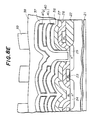
- FIG.8E shows a DRAM fabricated according to the seventh preferred embodiment of the present invention.
- a storage electrode 40 has two stacked polysilicon fins 401 and 402.
- the polysilicon fin 401 corresponds to the patterned polysilicon layers 29'' and 29' and the polysilicon sidewall 32
- the polysilicon fin 402 corresponds to the patterned polysilicon layer 42. It can be seen From FIG.6N and FIG.8E that the adjacent stacked capacitors shown in FIG.8E are closer to each other than those shown in FIG.6N.
- the first variation has a storage electrode having only the polysilicon fin 291 which consists of the polysilicon layers 29'' and 29' and the polysilicon sidewall 32.
- the polysilicon layer consisting of the polysilicon layers 29'' and 29' and the polysilicon sidewall 32 is patterned into the shape of the storage electrode. After that, the device is placed in an HF etchant, so that the insulating layer 28 is completely removed, as shown in FIG.9A.
- the insulating layer 27 can be formed of SiO2 or Si3N4.
- the fin 291 is thicker than a vertically extending portion of the storage electrode.
- FIG.10 illustrates a second variation of the aforementioned sixth preferred embodiment of the present invention.
- the polysilicon fin 291 consisting of the polysilicon layers 29'' and 29' and the polysilicon sidewall 32 is formed directly on the insulating layer 27 formed of SiO2 or Si3N4.
- the polysilicon layer 29' shown in FIG.6F is grown on the insulating layer 27 without forming the insulating layer 28. Then, the same steps as has been described with reference to FIGS.6G through 6K and FIG.6N are carried out. It is also possible to form the polysilicon fin 292 on the polysilicon fin 291 in the same way as has been described with reference to FIGS.6L and 6M.
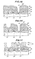
- FIGS.11A through 11J A description will now be given of an eighth preferred embodiment of the present invention with reference to FIGS.11A through 11J, in which those parts which are the same as shown shown in the previous figures are given the same reference numerals.
- a structure shown in FIG.11B is the same as that shown in FIG.6E. Steps to obtain the structure shown in FIG.11B are the same as those which have been described with reference to FIGS.6A through 6E.
- the Si3N4 insulating layer 27, the SiO2 spacer layer 28, the impurity-doped polysilicon layer 29', a spacer layer 45 formed of SiO2 and an impurity-doped polysilicon layer 46' are formed in this order by CVD. For example, each of these layers is 500 angstorms thick.
- the polysilicon layer 46', the SiO2 spacer layer 45 and the polysilicon layer 29' are selectively etched by the resist process and the RIE process, so that an opening 29A having a thickness equal to, for example, 0.6 ⁇ m is formed therein.
- a CCl4/O2 gas is used for the polysilicon layers 46' and 29', and a CHF3/He gas is used for the SiO2 spacer layer 45.
- a polysilicon layer 47' is grown to, for example, 2000 angstorms on the entire surface by CVD.
- the polysilicon layer 47' is anisotropically etched by an RIE process in which a CCl4/O2 gas or an HBr/He gas is used.
- a polysilicon sidewall 47 is formed around an inner surface of the opening 29A, and the remaining portion of the polysilicon layer 47' is removed.
- the sidewall 47 defines a new opening 46A having a width approximately equal to 0.2 - 0.3 ⁇ m, which is smaller than the width of the opening 29A shown in FIG.11C.
- the SiO2 spacer layer 28, the Si3N4 insulating layer 27, the SiO2 insulating layer 26 and the SiO2 gate insulating layer 23 are partially removed by an RIE process in which a CHF3/He gas is used and the polysilicon layer 46' and the polysilicon sidewall 47 function as etching masks.
- RIE process the surface of the n+-type drain region 25 is partially exposed through a contact hole 28A.
- the width of the opening 46A is very small and equal to about 0.2 - 0.3 ⁇ m, and that the polysilicon layer 46' and the polysilicon layer 47 functioning as the etching masks form a part of the storage electrode without being removed. Thus, it is not necessary to provide a special step to remove the polysilicon layer 46' and the polysilicon sidewall 47 functioning the etching masks.
- a polysilicon layer 46'' is grown to, for example, 500 angstroms by CVD. During this step, the polysilicon layers 46'' and 46' as well as the polysilicon sidewall 47 are integrated.
- the polysilicon layers 46''and 46', the SiO2 spacer layer 45, and the polysilicon layer 29' are patterned into the shape of the storage electrode in this order by the resist process using a single mask and the RIE process in the conventional photolithography process.
- the device shown in FIG.11H is placed in an HF etchant, so that the exposed SiO2 insulating layers are isotropically etched, so that a storage electrode 50 having two polysilicon fins 501 and 502 is formed.
- the fin 501 is formed of the patterned polysilicon layer 29'
- the fin 502 is formed of the patterned polysilicon layers 46'' and 46'.
- the fins 501 and 502 are connected by the polysilicon sidewall 47.
- the polysilicon layer 46'' which is a part of the fin 502 vertically extends from its portion on the polysilicon layer 46' and makes contact with the n+-type drain region 25.
- a vertical portion 503 of the storage electrode 50 consists of the polysilicon sidewall 47 and the polysilicon layer 46''.
- the vertical portion 503, the polysilicon layer 46'', and the fin 502 have mutually different thicknesses t1, t2 and t3, respectively.
- the vertical portion 503 is thicker than the polysilicon layer 46'' and the fin 502.
- the dielectric film 36, the cell plate 37, the PSG passivation layer 38 and the word-line shut layers 39 are formed in the same way as has been described with reference to FIG.6N.
- FIGS.12A through 12G A description will now be given of a ninth preferred embodiment of the present invention with reference to FIGS.12A through 12G, in which those parts which are the same as those shown in the previous figures are given the same reference numerals.
- FIGS.12A and 12B Production steps shown in FIGS.12A and 12B are carried out in the same way as those shown in FIGS.11A and 11B.
- the Si3N4 insulating layer 27, the SiO2 spacer layer 28, the impurity-doped polysilicon layer 29', the SiO2 spacer layer 45 and the impurity-doped polysilicon layer 46' are formed in this order by CVD.
- Each of these layers is 500 angstroms thick, for example.
- the polysilicon layer 46', the SiO2 spacer layer 45, the polysilicon layer 29' and the SiO2 spacer layer 28 are selectively etched by the resist process and RIE process, so that an opening 28A is formed therein.
- the SiO2 layer 28 is etched as shown in FIG.12C, while the SiO2 layer 28 shown in FIG.11C is not etched.
- a polysilicon layer 47' is grown to, for example, 2000 angstorms by CVD.
- the polysilicon layer 47' is selectively etched by an RIE process using a CCl4/O2 gas, so that a polysilicon sidewall 47a is formed so that it surrounds the inner wall of the opening 28A.
- the remaining portion of the polysilicon layer 47' is completely removed.
- the polysilicon sidewall 47a defines a new opening 46A narrower than the opening 28A.
- the Si3N4 insulating layer 27, the SiO2 insulating layer 26 and the SiO2 gate insulating layer 23 are selectively etched by an RIE process in which a CHF3/He gas is used and the polysilicon layer 46' and the sidewall 47a function as etching masks.
- RIE process a CHF3/He gas is used and the polysilicon layer 46' and the sidewall 47a function as etching masks.
- the surface of the n+-type drain region 25 is partially exposed through a through hole 27A having the same width as the opening 46A.
- the length of the sidewall 37a used in the ninth embodiment of the present invention is greater than that of the sidewall 37 used in the eighth embodiment of the present invention.
- the sidewall 47a functions as the mask more stably than the sidewall 47.
- the distance between the sidewall 37a and the word line WL is closer than the corresponding distance obtained in the eighth embodiment of the present invention.
- the breakdown voltage of the DRAM shown in FIG.12G is slightly smaller than that of the DRAM shown in FIG.11J.
- FIGS.13A and 13B are the same as FIGS.11A and 11B.
- the Si3N4 insulating layer 27, the SiO2 layer 28, the impurity-doped polysilicon layer 29', the SiO2 spacer layer 45 and the impurity-doped polysilicon layer 46' are formed in this order by the aforementioned process.
- an SiO2 insulating layer 48 is grown to, for example, 200 angstroms by CVD.
- the SiO2 layer 48, the polysilicon layer 46', the SiO2 spacer layer 45, the polysilicon layer 29' and the SiO2 spacer layer 28 are selectively removed, so that the surface of the Si3N4 layer 27 is partially exposed through the opening 28A.
- the polysilicon layer 47' is grown to, for example, 2000 angstorms by CVD.
- the polysilicon layer 47' is selectively etched by RIE, so that a widewall 42b is formed around an inner wall of the opening 28A.
- the Si3N4 layer 27, the SiO2 layer 26 and the SiO2 gate insulating layer 23 are selectively etched via the opening defined by the sidewall 47b.
- the SiO2 layer 48 is removed at the same time as the SiO2 insulating layer 26 is removed.
- the SiO2 layer 48 functions to protect the polysilicon layer 46' against the RIE process of forming the sidewall 47b. Further, the SiO2 layer 48 functions as the mask more stably during the time when the Si3N4 insulating layer 27 is being etched.
- FIGS.14A and 14B are the same as FIGS.11A and 11B, respectively.
- an SOG (spin on glass) layer 49 is formed on the entire surface so that the surface of the SOG layer 49 is substantially flat enough to prevent the growth of residuum during a subsequent process.
- residuum may be formed on a rough surface after the selective etching process.
- the SiO2 layer 48 may be partially left on a rough surface portion of the polysilicon layer 46'.
- FIG.14C shows that the SOG layer 49 is completely flat. It can be seen from FIG.14C, the SOG layer 49 absorbs a roughness of the surface shown in FIG.14B.
- the polysilicon layer 47' is grown to, for example, 2000 angstroms by CVD, and selectively etched by the RIE process, so that a sidewall 47b is formed, as shown in FIG.14E.
- the Si3N4 insulating layer 27, the SOG layer 49, the SiO2 layer 26 and the SiO2 layer 23 are selectively etched, so that the n+-type drain region 25 is partially exposed through the opening 27A.
- a DRAM shown in FIG.14G is fabricated by the aforementioned process which has been described with reference to FIG.6N.
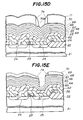
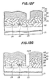
- FIGS.15A through 15J A description will now be given of a tenth preferred embodiment of the present invention with reference to FIGS.15A through 15J, in which those parts which are the same as those shown in the previous figures are given the same reference numerals.
- FIGS.15A and 15B are the same as FIG.11A and 11B, respectively.
- the first bilayer structure consists of an SiO2 insulating layer 63 and a polysilicon layer 64.
- the second bilayer structure consists of an SiO2 insulating layer 65 and a polysilicon layer 66.
- the third bilayer structure consists of an SiO2 insulating layer 67 and a polysilicon layer 68.
- an SiO2 insulating layer 69 having a thickness of 100 angstroms, a polysilicon layer 70 having a thickness of 2000 angstorms and an SiO2 insulating layer 71 having a thickness of 100 angstroms are successively grown in this order by CVD.
- a photoresist film 72 having a window pattern is placed on the SiO2 insulating layer 71, and the SiO2 insulating layer 71 and the polysilicon layer 70 are etched, so that an opening 70A is formed.
- the size of the opening 70A is approximately 0.5 ⁇ m, which is the scale limit in the conventional photolithography technique.
- the photoresist film 72 is removed, and a polysilicon layer is grown to, for example, 1500 angstroms on the entire surface. Then, the polysilicon layer is anisotropically etched by an RIE process using an HBr/He gas, so that a polysilicon sidewall 74 is formed around an inner wall of the opening 70A.
- the polysilicon sidewall 74 defines a new opening 70B having a size approximately equal to 0.2 ⁇ m.
- the SiO2 insulating layer 69 and the polysilicon layer 68 are anisotropically etched by an RIE process in which the polysilicon layer 70 and the sidewall 74 function as etching masks.
- the SiO2 insulating layer 71 is removed.
- the polysilicon layer 70 decreases by approximately 700 angstroms, so that a portion thereof having a thickness of about 1300 angstroms is left.
- the SiO2 insulating layer 67 is removed in an RIE process using a CHF3/H2 gas in which the polysilicon layer 70 and the sidewall 74 function as etching masks. During this etching process, there is little decrease in the thicknesses of the polysilicon layer 70 and the sidewall 74 because the CHF3/H2 gas acts to SiO2 greatly.
- the polysilicon layer 66 and the SiO2 insulating layer 65 are removed in the same way as has been described above. During this etching process, each of the polysilicon layer 70 and the sidewall 74 decreases by about 700 angstroms, so that they are approximately 600 angstroms thick.
- the polysilicon layer 64 is removed by RIE. During this RIE process, the polysilicon layer 70 and the sidewall 74 are also removed. It will be noted that the SiO2 insulating layer 69 prevents the underlying polysilicon layer 68 from being etched even if over-etching is carried out. It is preferable to carry out over-etching so that the polysilicon layer 70 and the sidewall 74 are completely removed.
- the SiO2 insulating layer 63 is removed in an etching process in which the polysilicon layer 68 functions as a mask. During this etching, the SiO2 insulating layer 69 is also removed. Subsequently, the Si3N4 insulating layer 62 is etched, and the SiO2 insulating layer 26 and SiO2 gate insulating layer 23 are etched. Thereby, a window formed in the layers 68 through 23 is formed, as shown in FIG.15G.
- a polysilicon layer 75 is grown to, for example, 500 angstroms on the entire surface including the window shown in FIG.15G.
- the polysilicon layers 75 and 68, the SiO2 insulating layer 67, the polysilicon layer 66, the SiO2 insulating layer 65, and the polysilicon layer 64 are patterned into the shape of the storage electrode. Thereby, a device shown in FIG.15H is formed.
- the storage electrode 90 has a first polysilicon fin 901 formed of the patterned polysilicon layer 64, a second polysilicon fin 902 formed of the patterned polysilicon layer 66, and a third polysilicon fin 903 having the patterned polysilicon layers 68 and 75, and a vertical connecting portion formed of the polysilicon layer 75.
- the third polysilicon fin 903 is thicker than the first and second polysilicon fins 901 and 902.
- the aforementioned processes are carried out for the device shown in FIG.15I, so that a DRAM shown in FIG.15J can be formed. It is possible to apply the teachings shown in FIGS.13A through 13F to the tenth embodiment of the present invention. It is also possible to form the lowermost fin9-1 directly on the insulating layer 62. In this case, the insulating layer 62 can be formed of SiO2.
Landscapes
- Engineering & Computer Science (AREA)
- Manufacturing & Machinery (AREA)
- Semiconductor Memories (AREA)
- Internal Circuitry In Semiconductor Integrated Circuit Devices (AREA)
Priority Applications (2)
| Application Number | Priority Date | Filing Date | Title |
|---|---|---|---|
| EP04008542A EP1465248A1 (de) | 1990-03-08 | 1991-03-06 | Schichtstruktur mit Kontaktloch und Verfahren zur Herstellung derselben |
| EP96118058A EP0764974B1 (de) | 1990-03-08 | 1991-03-06 | Schichtstruktur mit Kontaktöffnung und Verfahren zur Herstellung derselben |
Applications Claiming Priority (12)
| Application Number | Priority Date | Filing Date | Title |
|---|---|---|---|
| JP54883/90 | 1990-03-08 | ||
| JP2054883A JPH0824170B2 (ja) | 1990-03-08 | 1990-03-08 | 半導体記憶装置及びその製造方法 |
| JP5488390 | 1990-03-08 | ||
| JP2234585A JP2906350B2 (ja) | 1990-09-06 | 1990-09-06 | 半導体記憶装置及びその製造方法 |
| JP234585/90 | 1990-09-06 | ||
| JP23458590 | 1990-09-06 | ||
| JP28337190 | 1990-10-23 | ||
| JP28337090 | 1990-10-23 | ||
| JP2283371A JPH04158569A (ja) | 1990-10-23 | 1990-10-23 | 半導体記憶装置及びその製造方法 |
| JP2283370A JPH04158515A (ja) | 1990-10-23 | 1990-10-23 | 半導体装置の製造方法 |
| JP283370/90 | 1990-10-23 | ||
| JP283371/90 | 1990-10-23 |
Related Child Applications (1)
| Application Number | Title | Priority Date | Filing Date |
|---|---|---|---|
| EP96118058A Division EP0764974B1 (de) | 1990-03-08 | 1991-03-06 | Schichtstruktur mit Kontaktöffnung und Verfahren zur Herstellung derselben |
Publications (3)
| Publication Number | Publication Date |
|---|---|
| EP0449000A2 true EP0449000A2 (de) | 1991-10-02 |
| EP0449000A3 EP0449000A3 (en) | 1992-11-25 |
| EP0449000B1 EP0449000B1 (de) | 2004-08-18 |
Family
ID=27463125
Family Applications (3)
| Application Number | Title | Priority Date | Filing Date |
|---|---|---|---|
| EP96118058A Expired - Lifetime EP0764974B1 (de) | 1990-03-08 | 1991-03-06 | Schichtstruktur mit Kontaktöffnung und Verfahren zur Herstellung derselben |
| EP91103412A Expired - Lifetime EP0449000B1 (de) | 1990-03-08 | 1991-03-06 | Schichtstruktur mit Kontaktierungsöffnung für flossenförmige Kondensatoren in DRAMS und Methode zur Herstellung desselben |
| EP04008542A Withdrawn EP1465248A1 (de) | 1990-03-08 | 1991-03-06 | Schichtstruktur mit Kontaktloch und Verfahren zur Herstellung derselben |
Family Applications Before (1)
| Application Number | Title | Priority Date | Filing Date |
|---|---|---|---|
| EP96118058A Expired - Lifetime EP0764974B1 (de) | 1990-03-08 | 1991-03-06 | Schichtstruktur mit Kontaktöffnung und Verfahren zur Herstellung derselben |
Family Applications After (1)
| Application Number | Title | Priority Date | Filing Date |
|---|---|---|---|
| EP04008542A Withdrawn EP1465248A1 (de) | 1990-03-08 | 1991-03-06 | Schichtstruktur mit Kontaktloch und Verfahren zur Herstellung derselben |
Country Status (4)
| Country | Link |
|---|---|
| US (4) | US5705420A (de) |
| EP (3) | EP0764974B1 (de) |
| KR (1) | KR950014854B1 (de) |
| DE (2) | DE69133534T2 (de) |
Cited By (7)
| Publication number | Priority date | Publication date | Assignee | Title |
|---|---|---|---|---|
| DE4340419A1 (de) * | 1992-11-27 | 1994-06-01 | Mitsubishi Electric Corp | Halbleitervorrichtung und Herstellungsverfahren dafür |
| FR2704689A1 (fr) * | 1993-04-15 | 1994-11-04 | Samsung Electronics Co Ltd | Procédé de formation de motif fin dans un dispositif à semi-conducteur. |
| US5543339A (en) * | 1994-08-29 | 1996-08-06 | Motorola, Inc. | Process for forming an electrically programmable read-only memory cell |
| US5661340A (en) * | 1991-07-25 | 1997-08-26 | Fujitsu Limited | Dynamic random access memory having a stacked fin capacitor with reduced fin thickness |
| EP0973194A1 (de) * | 1998-07-13 | 2000-01-19 | Nec Corporation | Halbleiterbauelement und Verfahren zu dessen Herstellung |
| DE4345413C2 (de) * | 1992-11-27 | 2003-09-18 | Mitsubishi Electric Corp | Herstellungsverfahren für eine Halbleitervorrichtung mit einer Isolierschicht, in der ein Kontaktloch gebildet ist |
| DE4345300B4 (de) * | 1992-11-27 | 2005-02-10 | Mitsubishi Denki K.K. | Verfahren zum Herstellen einer MOS-Halbleitervorrichtung |
Families Citing this family (13)
| Publication number | Priority date | Publication date | Assignee | Title |
|---|---|---|---|---|
| EP0764974B1 (de) * | 1990-03-08 | 2006-06-14 | Fujitsu Limited | Schichtstruktur mit Kontaktöffnung und Verfahren zur Herstellung derselben |
| US6110833A (en) | 1998-03-03 | 2000-08-29 | Advanced Micro Devices, Inc. | Elimination of oxynitride (ONO) etch residue and polysilicon stringers through isolation of floating gates on adjacent bitlines by polysilicon oxidation |
| US5963840A (en) * | 1996-11-13 | 1999-10-05 | Applied Materials, Inc. | Methods for depositing premetal dielectric layer at sub-atmospheric and high temperature conditions |
| KR100233832B1 (ko) * | 1996-12-14 | 1999-12-01 | 정선종 | 반도체 소자의 트랜지스터 및 그 제조방법 |
| JPH11261025A (ja) * | 1998-03-13 | 1999-09-24 | Fujitsu Ltd | 半導体装置の製造方法 |
| US6083790A (en) * | 1999-02-11 | 2000-07-04 | Taiwan Semiconductor Manufacturing Company Ltd. | Method for making y-shaped multi-fin stacked capacitors for dynamic random access memory cells |
| US20040077174A1 (en) * | 2002-10-18 | 2004-04-22 | Chartered Semiconductor Manufacturing Ltd. | Method for forming a high aspect ratio via |
| DE102004001853B3 (de) * | 2004-01-13 | 2005-07-21 | Infineon Technologies Ag | Verfahren zum Herstellen von Kontaktierungsanschlüssen |
| US20090096003A1 (en) * | 2007-10-11 | 2009-04-16 | International Business Machines Corporation | Semiconductor cell structure including buried capacitor and method for fabrication thereof |
| CN102326248B (zh) * | 2009-02-25 | 2014-06-25 | 日本电气株式会社 | 电容器制造方法、电容器制造装置 |
| EP2546321A4 (de) * | 2010-03-12 | 2014-05-14 | Bridgestone Corp | Lichtemittierender körper mit silicium-mikropartikeln und verfahren zur herstellung eines lichtemittierender körpers mit silicium-mikropartikeln |
| US9117690B2 (en) * | 2011-12-02 | 2015-08-25 | Unisantis Electronics Singapore Pte. Ltd. | Method for producing semiconductor device and semiconductor device |
| KR101934426B1 (ko) * | 2012-11-26 | 2019-01-03 | 삼성전자 주식회사 | 반도체 장치 및 그 제조 방법 |
Family Cites Families (40)
| Publication number | Priority date | Publication date | Assignee | Title |
|---|---|---|---|---|
| US4256514A (en) * | 1978-11-03 | 1981-03-17 | International Business Machines Corporation | Method for forming a narrow dimensioned region on a body |
| JPS566628A (en) * | 1979-06-26 | 1981-01-23 | Hitachi Ltd | Power decision signal generator circuit |
| JPS57199221A (en) * | 1981-06-02 | 1982-12-07 | Toshiba Corp | Manufacture of semiconductor device |
| JPS60106163A (ja) * | 1983-11-15 | 1985-06-11 | Fujitsu Ltd | 半導体装置の製造方法 |
| JPS60224218A (ja) * | 1984-04-20 | 1985-11-08 | Toshiba Corp | 半導体装置の製造方法 |
| US4589196A (en) * | 1984-10-11 | 1986-05-20 | Texas Instruments Incorporated | Contacts for VLSI devices using direct-reacted silicide |
| JPS61193477A (ja) * | 1985-02-22 | 1986-08-27 | Hitachi Ltd | 半導体記憶装置 |
| DE122007000007I2 (de) | 1986-04-09 | 2010-12-30 | Genzyme Corp | Genetisch transformierte Tiere, die ein gewünschtes Protein in Milch absondern |
| US4707218A (en) * | 1986-10-28 | 1987-11-17 | International Business Machines Corporation | Lithographic image size reduction |
| JPS63119239A (ja) * | 1986-11-06 | 1988-05-23 | Fujitsu Ltd | 半導体装置の製造方法 |
| EP0280587A1 (de) * | 1987-01-20 | 1988-08-31 | Thomson Components-Mostek Corporation | VLSI-Verfahren unter Verwendung einer Maske mit Distanzstücken |
| JPS63253661A (ja) * | 1987-04-10 | 1988-10-20 | Oki Electric Ind Co Ltd | 半導体記憶装置の製造方法 |
| JPS63291437A (ja) * | 1987-05-25 | 1988-11-29 | Toshiba Corp | 半導体装置 |
| JP2627515B2 (ja) * | 1987-12-10 | 1997-07-09 | 富士通株式会社 | 半導体記憶装置及びその製造方法 |
| JP2642364B2 (ja) * | 1987-12-03 | 1997-08-20 | 富士通株式会社 | 半導体記憶装置及びその製造方法 |
| DE3856143T2 (de) * | 1987-06-17 | 1998-10-29 | Fujitsu Ltd | Verfahren zum Herstellen einer dynamischen Speicherzelle mit wahlfreiem Zugriff |
| JPS6422057A (en) * | 1987-07-17 | 1989-01-25 | Matsushita Electric Industrial Co Ltd | Manufacture of multi-layer planar type capacitor |
| KR910009805B1 (ko) * | 1987-11-25 | 1991-11-30 | 후지쓰 가부시끼가이샤 | 다이나믹 랜덤 액세스 메모리 장치와 그의 제조방법 |
| JP2772375B2 (ja) * | 1987-11-25 | 1998-07-02 | 富士通株式会社 | 半導体記憶装置 |
| JPH01140761A (ja) * | 1987-11-27 | 1989-06-01 | Nec Corp | 半導体装置 |
| JP2590171B2 (ja) * | 1988-01-08 | 1997-03-12 | 株式会社日立製作所 | 半導体記憶装置 |
| JPH01189949A (ja) * | 1988-01-26 | 1989-07-31 | Fujitsu Ltd | 半導体記憶装置の製造方法 |
| US4872050A (en) * | 1988-03-15 | 1989-10-03 | Mitsubishi Denki Kabushiki Kaisha | Interconnection structure in semiconductor device and manufacturing method of the same |
| JP2670288B2 (ja) * | 1988-03-24 | 1997-10-29 | 株式会社東芝 | 半導体装置の製造方法 |
| JP2776826B2 (ja) * | 1988-04-15 | 1998-07-16 | 株式会社日立製作所 | 半導体装置およびその製造方法 |
| JPH01265556A (ja) * | 1988-04-15 | 1989-10-23 | Fujitsu Ltd | 半導体記憶装置及びその製造方法 |
| JPH01270343A (ja) * | 1988-04-22 | 1989-10-27 | Fujitsu Ltd | 半導体装置の製造方法 |
| KR900019227A (ko) * | 1988-05-18 | 1990-12-24 | 아오이 죠이치 | 적층형 캐피시터를 갖춘 반도체기억장치 및 그 제조방법 |
| KR910010167B1 (ko) * | 1988-06-07 | 1991-12-17 | 삼성전자 주식회사 | 스택 캐패시터 dram셀 및 그의 제조방법 |
| JPH0744186B2 (ja) * | 1989-03-13 | 1995-05-15 | 株式会社東芝 | 半導体装置の製造方法 |
| KR900015320A (ko) * | 1989-03-17 | 1990-10-26 | 정몽헌 | 트렌치 미세패턴 형성방법 |
| JPH02250239A (ja) * | 1989-03-23 | 1990-10-08 | Tohoku Gakuin Univ | 陰極線管 |
| US4970562A (en) * | 1989-05-22 | 1990-11-13 | Xerox Corporation | Color image processing apparatus |
| JPH0338061A (ja) * | 1989-07-05 | 1991-02-19 | Fujitsu Ltd | 半導体記憶装置 |
| US5279990A (en) * | 1990-03-02 | 1994-01-18 | Motorola, Inc. | Method of making a small geometry contact using sidewall spacers |
| EP0764974B1 (de) * | 1990-03-08 | 2006-06-14 | Fujitsu Limited | Schichtstruktur mit Kontaktöffnung und Verfahren zur Herstellung derselben |
| KR920001760A (ko) * | 1990-06-29 | 1992-01-30 | 김광호 | 디램셀의 적층형 캐패시터 제조방법 |
| US5262352A (en) * | 1992-08-31 | 1993-11-16 | Motorola, Inc. | Method for forming an interconnection structure for conductive layers |
| JP3271094B2 (ja) * | 1993-07-05 | 2002-04-02 | ソニー株式会社 | 積層配線基板及びその製造方法 |
| US5874359A (en) * | 1995-04-27 | 1999-02-23 | Industrial Technology Research Institute | Small contacts for ultra large scale integration semiconductor devices without separation ground rule |
-
1991
- 1991-03-06 EP EP96118058A patent/EP0764974B1/de not_active Expired - Lifetime
- 1991-03-06 DE DE69133534T patent/DE69133534T2/de not_active Expired - Fee Related
- 1991-03-06 EP EP91103412A patent/EP0449000B1/de not_active Expired - Lifetime
- 1991-03-06 EP EP04008542A patent/EP1465248A1/de not_active Withdrawn
- 1991-03-06 DE DE69133410T patent/DE69133410T2/de not_active Expired - Fee Related
- 1991-03-08 KR KR1019910003763A patent/KR950014854B1/ko not_active Expired - Fee Related
-
1995
- 1995-05-26 US US08/451,904 patent/US5705420A/en not_active Expired - Fee Related
- 1995-05-30 US US08/453,509 patent/US6144058A/en not_active Expired - Fee Related
-
2000
- 2000-09-21 US US09/666,842 patent/US6528369B1/en not_active Expired - Fee Related
-
2003
- 2003-01-30 US US10/354,088 patent/US20030134470A1/en not_active Abandoned
Cited By (12)
| Publication number | Priority date | Publication date | Assignee | Title |
|---|---|---|---|---|
| US5661340A (en) * | 1991-07-25 | 1997-08-26 | Fujitsu Limited | Dynamic random access memory having a stacked fin capacitor with reduced fin thickness |
| EP0528183B1 (de) * | 1991-07-25 | 1997-10-08 | Fujitsu Limited | Verfahren zur Herstellung eines dynamischen RAM mit Kondensator mit gestapelter Flossenstruktur und reduzierter Flossendicke |
| DE4340419A1 (de) * | 1992-11-27 | 1994-06-01 | Mitsubishi Electric Corp | Halbleitervorrichtung und Herstellungsverfahren dafür |
| DE4340419C2 (de) * | 1992-11-27 | 1998-11-12 | Mitsubishi Electric Corp | Herstellungsverfahren für eine Halbleitervorrichtung mit einer Isolierschicht, in der ein Kontaktloch gebildet ist |
| US6097052A (en) * | 1992-11-27 | 2000-08-01 | Mitsubishi Denki Kabushiki Kaisha | Semiconductor device and a method of manufacturing thereof |
| US6586329B1 (en) | 1992-11-27 | 2003-07-01 | Mitsubishi Denki Kabshiki Kaisha | Semiconductor device and a method of manufacturing thereof |
| DE4345413C2 (de) * | 1992-11-27 | 2003-09-18 | Mitsubishi Electric Corp | Herstellungsverfahren für eine Halbleitervorrichtung mit einer Isolierschicht, in der ein Kontaktloch gebildet ist |
| DE4345300B4 (de) * | 1992-11-27 | 2005-02-10 | Mitsubishi Denki K.K. | Verfahren zum Herstellen einer MOS-Halbleitervorrichtung |
| FR2704689A1 (fr) * | 1993-04-15 | 1994-11-04 | Samsung Electronics Co Ltd | Procédé de formation de motif fin dans un dispositif à semi-conducteur. |
| US5543339A (en) * | 1994-08-29 | 1996-08-06 | Motorola, Inc. | Process for forming an electrically programmable read-only memory cell |
| US5616941A (en) * | 1994-08-29 | 1997-04-01 | Motorola Inc. | Electrically programmable read-only memory cell |
| EP0973194A1 (de) * | 1998-07-13 | 2000-01-19 | Nec Corporation | Halbleiterbauelement und Verfahren zu dessen Herstellung |
Also Published As
| Publication number | Publication date |
|---|---|
| DE69133534T2 (de) | 2006-12-28 |
| US6528369B1 (en) | 2003-03-04 |
| DE69133410T2 (de) | 2005-09-08 |
| KR950014854B1 (ko) | 1995-12-16 |
| DE69133534D1 (de) | 2006-07-27 |
| EP1465248A1 (de) | 2004-10-06 |
| US6144058A (en) | 2000-11-07 |
| EP0764974B1 (de) | 2006-06-14 |
| DE69133410D1 (de) | 2004-09-23 |
| EP0449000A3 (en) | 1992-11-25 |
| US20030134470A1 (en) | 2003-07-17 |
| EP0449000B1 (de) | 2004-08-18 |
| US5705420A (en) | 1998-01-06 |
| EP0764974A1 (de) | 1997-03-26 |
Similar Documents
| Publication | Publication Date | Title |
|---|---|---|
| US6144058A (en) | Layer structure having contact hole, method of producing the same, fin-shaped capacitor using the layer structure, method of producing the fin-shaped capacitor and dynamic random access memory having the fin-shaped capacitor | |
| US5296400A (en) | Method of manufacturing a contact of a highly integrated semiconductor device | |
| US5394012A (en) | Semiconductor device and manufacturing method of the same | |
| US7153727B2 (en) | Semiconductor device and method of manufacturing the same | |
| US4953126A (en) | Dynamic random access memory device including a stack capacitor | |
| KR100295566B1 (ko) | 반도체장치와그제조방법,및반도체기억장치와그제조방법 | |
| KR0155886B1 (ko) | 고집적 dram 셀의 제조방법 | |
| US6770527B2 (en) | Semiconductor integrated circuit device and method of manufacturing the same | |
| US5936272A (en) | DRAM transistor cells with a self-aligned storage electrode contact | |
| JP3562895B2 (ja) | ランディングパッドを有する半導体装置の製造方法 | |
| US5525534A (en) | Method of producing a semiconductor device using a reticle having a polygonal shaped hole | |
| US6475858B2 (en) | Method of manufacturing semiconductor device | |
| KR0151866B1 (ko) | 반도체 장치 및 그 제조방법 | |
| US5723381A (en) | Formation of self-aligned overlapping bitline contacts with sacrificial polysilicon fill-in stud | |
| US5597763A (en) | Method for manufacturing a semiconductor wiring structure including a self-aligned contact hole | |
| US20020034877A1 (en) | Method of forming a self-aligned contact, and method of fabricating a semiconductor device having a self-aligned contact | |
| US5631184A (en) | Method of producing a semiconductor device having a fin type capacitor | |
| US5332687A (en) | Method of manufacturing a semiconductor memory having a memory cell array and a peripheral circuit portion so as to improve the characteristics of the device | |
| US6369423B2 (en) | Semiconductor device with a thin gate stack having a plurality of insulating layers | |
| US20010045666A1 (en) | Semiconductor device having self-aligned contact and fabricating method therefor | |
| US6136716A (en) | Method for manufacturing a self-aligned stacked storage node DRAM cell | |
| JP3190659B2 (ja) | 半導体メモリ及びその製造方法 | |
| JPH0637273A (ja) | 半導体装置とその製造方法 | |
| JP3498022B2 (ja) | 半導体装置の製造方法 | |
| JP3172229B2 (ja) | 半導体装置の製造方法 |
Legal Events
| Date | Code | Title | Description |
|---|---|---|---|
| PUAI | Public reference made under article 153(3) epc to a published international application that has entered the european phase |
Free format text: ORIGINAL CODE: 0009012 |
|
| AK | Designated contracting states |
Kind code of ref document: A2 Designated state(s): DE FR GB IT |
|
| PUAL | Search report despatched |
Free format text: ORIGINAL CODE: 0009013 |
|
| AK | Designated contracting states |
Kind code of ref document: A3 Designated state(s): DE FR GB IT |
|
| 17P | Request for examination filed |
Effective date: 19930525 |
|
| 17Q | First examination report despatched |
Effective date: 19950105 |
|
| APAB | Appeal dossier modified |
Free format text: ORIGINAL CODE: EPIDOS NOAPE |
|
| APAB | Appeal dossier modified |
Free format text: ORIGINAL CODE: EPIDOS NOAPE |
|
| APAD | Appeal reference recorded |
Free format text: ORIGINAL CODE: EPIDOS REFNE |
|
| GRAP | Despatch of communication of intention to grant a patent |
Free format text: ORIGINAL CODE: EPIDOSNIGR1 |
|
| GRAS | Grant fee paid |
Free format text: ORIGINAL CODE: EPIDOSNIGR3 |
|
| GRAA | (expected) grant |
Free format text: ORIGINAL CODE: 0009210 |
|
| AK | Designated contracting states |
Kind code of ref document: B1 Designated state(s): DE FR GB IT |
|
| DX | Miscellaneous (deleted) | ||
| REG | Reference to a national code |
Ref country code: GB Ref legal event code: FG4D |
|
| REF | Corresponds to: |
Ref document number: 69133410 Country of ref document: DE Date of ref document: 20040923 Kind code of ref document: P |
|
| PG25 | Lapsed in a contracting state [announced via postgrant information from national office to epo] |
Ref country code: GB Free format text: LAPSE BECAUSE OF NON-PAYMENT OF DUE FEES Effective date: 20050306 |
|
| ET | Fr: translation filed | ||
| PLBE | No opposition filed within time limit |
Free format text: ORIGINAL CODE: 0009261 |
|
| STAA | Information on the status of an ep patent application or granted ep patent |
Free format text: STATUS: NO OPPOSITION FILED WITHIN TIME LIMIT |
|
| 26N | No opposition filed |
Effective date: 20050519 |
|
| APAH | Appeal reference modified |
Free format text: ORIGINAL CODE: EPIDOSCREFNO |
|
| GBPC | Gb: european patent ceased through non-payment of renewal fee |
Effective date: 20050306 |
|
| PGFP | Annual fee paid to national office [announced via postgrant information from national office to epo] |
Ref country code: IT Payment date: 20080327 Year of fee payment: 18 |
|
| PGFP | Annual fee paid to national office [announced via postgrant information from national office to epo] |
Ref country code: FR Payment date: 20080311 Year of fee payment: 18 Ref country code: DE Payment date: 20080228 Year of fee payment: 18 |
|
| REG | Reference to a national code |
Ref country code: FR Ref legal event code: ST Effective date: 20091130 |
|
| PG25 | Lapsed in a contracting state [announced via postgrant information from national office to epo] |
Ref country code: DE Free format text: LAPSE BECAUSE OF NON-PAYMENT OF DUE FEES Effective date: 20091001 |
|
| PG25 | Lapsed in a contracting state [announced via postgrant information from national office to epo] |
Ref country code: FR Free format text: LAPSE BECAUSE OF NON-PAYMENT OF DUE FEES Effective date: 20091123 |
|
| PG25 | Lapsed in a contracting state [announced via postgrant information from national office to epo] |
Ref country code: IT Free format text: LAPSE BECAUSE OF NON-PAYMENT OF DUE FEES Effective date: 20090306 |