EP0450496A1 - Infrarotsensor - Google Patents
Infrarotsensor Download PDFInfo
- Publication number
- EP0450496A1 EP0450496A1 EP91104917A EP91104917A EP0450496A1 EP 0450496 A1 EP0450496 A1 EP 0450496A1 EP 91104917 A EP91104917 A EP 91104917A EP 91104917 A EP91104917 A EP 91104917A EP 0450496 A1 EP0450496 A1 EP 0450496A1
- Authority
- EP
- European Patent Office
- Prior art keywords
- signal processing
- processing circuit
- infrared sensor
- aluminum film
- substrate
- Prior art date
- Legal status (The legal status is an assumption and is not a legal conclusion. Google has not performed a legal analysis and makes no representation as to the accuracy of the status listed.)
- Granted
Links
Images


Classifications
-
- H—ELECTRICITY
- H10—SEMICONDUCTOR DEVICES; ELECTRIC SOLID-STATE DEVICES NOT OTHERWISE PROVIDED FOR
- H10F—INORGANIC SEMICONDUCTOR DEVICES SENSITIVE TO INFRARED RADIATION, LIGHT, ELECTROMAGNETIC RADIATION OF SHORTER WAVELENGTH OR CORPUSCULAR RADIATION
- H10F77/00—Constructional details of devices covered by this subclass
- H10F77/20—Electrodes
- H10F77/206—Electrodes for devices having potential barriers
-
- H—ELECTRICITY
- H10—SEMICONDUCTOR DEVICES; ELECTRIC SOLID-STATE DEVICES NOT OTHERWISE PROVIDED FOR
- H10F—INORGANIC SEMICONDUCTOR DEVICES SENSITIVE TO INFRARED RADIATION, LIGHT, ELECTROMAGNETIC RADIATION OF SHORTER WAVELENGTH OR CORPUSCULAR RADIATION
- H10F77/00—Constructional details of devices covered by this subclass
- H10F77/30—Coatings
- H10F77/306—Coatings for devices having potential barriers
- H10F77/331—Coatings for devices having potential barriers for filtering or shielding light, e.g. multicolour filters for photodetectors
- H10F77/334—Coatings for devices having potential barriers for filtering or shielding light, e.g. multicolour filters for photodetectors for shielding light, e.g. light blocking layers or cold shields for infrared detectors
-
- H—ELECTRICITY
- H10—SEMICONDUCTOR DEVICES; ELECTRIC SOLID-STATE DEVICES NOT OTHERWISE PROVIDED FOR
- H10W—GENERIC PACKAGES, INTERCONNECTIONS, CONNECTORS OR OTHER CONSTRUCTIONAL DETAILS OF DEVICES COVERED BY CLASS H10
- H10W90/00—Package configurations
- H10W90/701—Package configurations characterised by the relative positions of pads or connectors relative to package parts
- H10W90/751—Package configurations characterised by the relative positions of pads or connectors relative to package parts of bond wires
- H10W90/756—Package configurations characterised by the relative positions of pads or connectors relative to package parts of bond wires between a chip and a stacked lead frame, conducting package substrate or heat sink
Definitions
- the present invention relates to an infrared sensor and, more particularly, to a remote infrared sensor suitable for use on television receivers and tape recorders including video tape recorders.
- Recent television receivers and VTRs are provided with a remote infrared sensor which receives and processes control signals provided by a remote controller.
- the conventional remote infrared sensor employs a photodetector including a pin diode.
- the conventional remote infrared sensor comprises a sensing unit having a photodetector employing a pin photodiode, a signal processing circuit comprising a signal amplifier and a frequency band controller, and a metallic box accommodating the sensing unit and the signal processing circuit.
- This conventional remote infrared sensor comprises about ten component parts and requires assembling processes for assembling those component parts. Therefore, it is difficult to fabricate the remote infrared sensor at a high productivity and to reduce the cost.
- Fig. 4 shows a previously proposed remote infrared sensor B intended to improve the productivity of the manufacturing process and to reduce the cost.
- the remote infrared sensor B is a monolithic remote infrared sensor comprising: a p-type silicon substrate 22; a photodetector 21 comprising a plurality of pn junctions formed, for example, by forming a p-type diffused region on an n-type epitaxial layer on the p-type silicon substrate 22; a signal processing circuit 23 formed on the p-type silicon substrate 22; and bonding pads 24.
- This remote infrared sensor B can be fabricated at a high productivity and at a relatively low cost.
- the present invention has been made in view of such a problem, and it is therefore an object of the present invention to provide an infrared sensor having a signal processing circuit, and capable of preventing the penetration of infrared radiation into the signal processing circuit to suppress the generation of noise due to the penetration of infrared radiation into the signal processing circuit.
- an infrared sensor comprises a substrate, a sensing unit formed on the substrate, and a signal processing circuit formed on the substrate, and characterized in that at least the signal processing circuit is covered with a conductive film.
- At least the signal processing circuit formed on the substrate on which the sensing unit is formed is covered with the conductive film which serves as a shield to intercept infrared radiation so that the infrared radiation may not penetrate into the signal processing circuit.
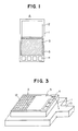
- Fig. 1 is a plan view of an infrared sensor A embodying the present invention.
- the infrared sensor A comprises a single silicon substrate 1, a photodetector 2, i.e., a sensing unit, comprising a photodiode and formed on the silicon substrate 1, a signal processing circuit 3 comprising an amplifier for amplifying an infinitesimal signal provided by the photodetector 2, and a frequency band controller, bonding pads 4 formed on the silicon substrate 1, and a conductive film 5 covering the signal processing circuit 3.
- a first aluminum film and a second aluminum film are formed one over the other. The first aluminum film is used for forming wiring patterns for the signal processing circuit 3, and the second aluminum film is used as both the conductive film 5 for preventing the penetration of infrared radiation into the signal processing circuit 3 and a grounding electrode for the signal processing circuit 3.
- portions of the second aluminum film 5 are used also for forming intersecting wiring patterns as shown in Fig. 2D when intersecting wiring patterns are necessary.
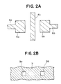
- a first wiring pattern 6a and a second wiring pattern 6b are formed opposite to each other and a third wiring pattern 6c is formed between the first wiring pattern 6a and the second wiring pattern 6b as shown in Fig. 2A by patterning the first aluminum film.
- an insulating film 7 is formed over the entire surface of the layer including the wiring patterns 6a, 6b and 6c, contact holes 9a and 9b are formed in the insulating film 7 at positions respectively corresponding to the terminal 8a of the first wiring pattern 6a and the terminal 8b of the second wiring pattern 6b as shown in Fig. 2B, the second aluminum film 5 is formed over the entire surface of the insulating film 7, and then the second aluminum film 5 is subjected to a patterning process to form a region 5a interconnecting the two contact holes 9a and 9b to connect electrically the first wiring pattern 6a and the second wiring pattern 6b shown in Fig. 2A by the region 5a.
- gaps a are formed in the second aluminum film 5 as shown in Fig. 2D, the generation of noise which may cause malfunction will not occur because the gaps aware very small.
- the function of the signal processing circuit 3 may hardly be affected by the penetration of infrared radiation through the gaps a into the signal processing circuit 3 if the front half of the signal processing circuit 3, in which an infinitesimal signal provided by the photodetector 2 is processed, is covered perfectly by the conductive film, i.e., the second aluminum film 5, and the gaps a are formed in the back half of the signal processing circuit 3, in which an amplified signal is processed, in connecting the wiring patterns of the first aluminum film by the wiring patterns of the second aluminum film 5.
- the second aluminum film 5 functions as an electromagnetic shield when the second aluminum film 5 of the infrared sensor A is connected to one of the bonding pads 4, and the boding pad 4 connected to the second aluminum film 5 is connected electrically to a lead frame 10 by a bonding wire 11 as shown in Fig. 3 to equalize the respective potentials of the second aluminum film 5 and the lead frame 10. Since the infrared sensor A is sandwiched between the second aluminum film 5 and the lead frame 10, the lines of electric force of an external electric field are able hardly to penetrate the infrared sensor A, so that the influence of the external electric field on the function of the infrared sensor A is reduced.
- the photodetector 2 and the signal processing circuit 3 are formed on the substrate 1, the number of component parts of the infrared sensor A is reduced to a minimum, and hence the infrared sensor A can be manufactured at a high productivity and at a relatively low cost.
- the signal processing circuit 3 is covered entirely with the conductive film, i.e., the second aluminum film 5, the penetration of infrared radiation into the signal processing circuit 3 is prevented to reduce the generation of noise due to the penetration of infrared radiation into the signal processing circuit 3 can be reduced.
- the second aluminum film 5 is used also as a grounding electrode and portions of the second aluminum film 5 are used as jumpers for the wiring patterns formed by the first aluminum film, any grounding line need not be included in the wiring patterns of the first aluminum film in designing the layout of the wiring patterns and the entire surface of the chip can effectively used, which facilitates designing the layout of the wiring patterns and increases the degree of freedom of designing the layout.
- the second aluminum film 5 and the lead frame 10 are equipotential and sandwich the infrared sensor A therebetween, the second aluminum film 5 and the lead frame 10 serve as both an electromagnetic shield and an electric field shield. Accordingly, the influence of an electromagnetic field and an electric field created, for example, by a television receiver or a VTR on the performance of the signal processing circuit 3 can be suppressed.
- the second aluminum film 5 in this embodiment is formed over the signal processing circuit 3
- the second aluminum film 5 may be formed over the entire surfaces of the photodetector 2 and the signal processing circuit 3 excluding the bonding pads 4, and a region of the second aluminum film 5 covering the photodetector 2 may be patterned to form a plurality of apertures 12 as shown in Fig. 3.
- Such a configuration enables the second aluminum film 5 function as an electromagnetic shield without reducing the quantity of incident infrared radiation on the photodetector 2 and reduces efficiently the influence of the external magnetic field created by a television receiver or a VTR on the performance of the photodetector 2.
- the infrared sensor in accordance with the present invention has a construction capable of preventing the penetration of infrared radiation into the signal processing circuit to suppress the generation of noise due to the penetration of infrared radiation into the signal processing circuit.
Landscapes
- Light Receiving Elements (AREA)
- Photometry And Measurement Of Optical Pulse Characteristics (AREA)
- Solid State Image Pick-Up Elements (AREA)
Applications Claiming Priority (2)
| Application Number | Priority Date | Filing Date | Title |
|---|---|---|---|
| JP2081709A JP3038772B2 (ja) | 1990-03-29 | 1990-03-29 | 赤外線センサ |
| JP81709/90 | 1990-03-29 |
Publications (2)
| Publication Number | Publication Date |
|---|---|
| EP0450496A1 true EP0450496A1 (de) | 1991-10-09 |
| EP0450496B1 EP0450496B1 (de) | 1996-11-27 |
Family
ID=13753918
Family Applications (1)
| Application Number | Title | Priority Date | Filing Date |
|---|---|---|---|
| EP91104917A Expired - Lifetime EP0450496B1 (de) | 1990-03-29 | 1991-03-27 | Infrarotsensor |
Country Status (4)
| Country | Link |
|---|---|
| US (1) | US5243192A (de) |
| EP (1) | EP0450496B1 (de) |
| JP (1) | JP3038772B2 (de) |
| DE (1) | DE69123276T2 (de) |
Cited By (3)
| Publication number | Priority date | Publication date | Assignee | Title |
|---|---|---|---|---|
| WO1993020588A1 (en) * | 1992-04-03 | 1993-10-14 | Asea Brown Boveri Ab | Detector circuit with a semiconductor diode operating as a detector and with an amplifier circuit integrated with the diode |
| EP0590598A1 (de) * | 1992-09-28 | 1994-04-06 | Sanyo Electric Co., Limited. | Halbeiter-Photodiode mit einer lichtundurchlässigen Schicht |
| US8187908B2 (en) | 2007-10-30 | 2012-05-29 | X-Fab Semiconductor Foundries Ag | Light-blocking layer sequence having one or more metal layers for an integrated circuit and method for the production of the layer sequence |
Families Citing this family (4)
| Publication number | Priority date | Publication date | Assignee | Title |
|---|---|---|---|---|
| JP2925943B2 (ja) * | 1994-08-31 | 1999-07-28 | 三洋電機株式会社 | ホトダイオード内蔵半導体装置 |
| WO1997023909A1 (fr) * | 1995-12-22 | 1997-07-03 | Sanyo Electric Co., Ltd. | Circuit integre incorporant une photodiode |
| US7224910B2 (en) * | 2002-10-25 | 2007-05-29 | Gennum Corporation | Direct attach optical receiver module and method of testing |
| CN100377360C (zh) * | 2004-04-14 | 2008-03-26 | 亚泰影像科技股份有限公司 | 影像感测器 |
Citations (3)
| Publication number | Priority date | Publication date | Assignee | Title |
|---|---|---|---|---|
| GB2097581A (en) * | 1981-04-24 | 1982-11-03 | Hitachi Ltd | Shielding semiconductor integrated circuit devices from light |
| EP0285084A2 (de) * | 1987-03-31 | 1988-10-05 | Kabushiki Kaisha Toshiba | Festkörperbildsensor |
| EP0364163A2 (de) * | 1988-10-14 | 1990-04-18 | AT&T Corp. | Elektrooptische Anordnung mit undurchsichtigen Schutzschichten |
-
1990
- 1990-03-29 JP JP2081709A patent/JP3038772B2/ja not_active Expired - Fee Related
-
1991
- 1991-03-27 EP EP91104917A patent/EP0450496B1/de not_active Expired - Lifetime
- 1991-03-27 DE DE69123276T patent/DE69123276T2/de not_active Expired - Fee Related
- 1991-03-28 US US07/676,545 patent/US5243192A/en not_active Expired - Lifetime
Patent Citations (3)
| Publication number | Priority date | Publication date | Assignee | Title |
|---|---|---|---|---|
| GB2097581A (en) * | 1981-04-24 | 1982-11-03 | Hitachi Ltd | Shielding semiconductor integrated circuit devices from light |
| EP0285084A2 (de) * | 1987-03-31 | 1988-10-05 | Kabushiki Kaisha Toshiba | Festkörperbildsensor |
| EP0364163A2 (de) * | 1988-10-14 | 1990-04-18 | AT&T Corp. | Elektrooptische Anordnung mit undurchsichtigen Schutzschichten |
Non-Patent Citations (1)
| Title |
|---|
| SENSOR AND ACTUATORS, vol. 11, no. 3, April 1987, LAUSANNE CH, pages 239 - 250; H. Verriele et al.: "A planar monolithic integrated photoreceiver: Association of a GaAs Schottky photodiode with a GaAs FET" * |
Cited By (3)
| Publication number | Priority date | Publication date | Assignee | Title |
|---|---|---|---|---|
| WO1993020588A1 (en) * | 1992-04-03 | 1993-10-14 | Asea Brown Boveri Ab | Detector circuit with a semiconductor diode operating as a detector and with an amplifier circuit integrated with the diode |
| EP0590598A1 (de) * | 1992-09-28 | 1994-04-06 | Sanyo Electric Co., Limited. | Halbeiter-Photodiode mit einer lichtundurchlässigen Schicht |
| US8187908B2 (en) | 2007-10-30 | 2012-05-29 | X-Fab Semiconductor Foundries Ag | Light-blocking layer sequence having one or more metal layers for an integrated circuit and method for the production of the layer sequence |
Also Published As
| Publication number | Publication date |
|---|---|
| EP0450496B1 (de) | 1996-11-27 |
| DE69123276D1 (de) | 1997-01-09 |
| JPH03280567A (ja) | 1991-12-11 |
| US5243192A (en) | 1993-09-07 |
| JP3038772B2 (ja) | 2000-05-08 |
| DE69123276T2 (de) | 1997-06-12 |
Similar Documents
| Publication | Publication Date | Title |
|---|---|---|
| US20030025824A1 (en) | Image pickup device incorporating a position defining member | |
| US7071523B2 (en) | Encapsulated light receiving and processing semiconductor module with enhanced shielding and grounding properties | |
| JPH0350859A (ja) | Loc型リードフレームを備えた半導体集積回路装置 | |
| US5243192A (en) | Infrared sensor | |
| US6781108B2 (en) | Noise canceling photosensor-amplifier device | |
| US5291054A (en) | Light receiving module for converting light signal to electric signal | |
| JP2973646B2 (ja) | ベアチップlsiの実装構造 | |
| JPH1168029A (ja) | 半導体装置 | |
| KR100516950B1 (ko) | 포토다이오드 | |
| US6649949B2 (en) | Photodiode with electrode for noise immunity | |
| JP2926818B2 (ja) | 光センサ | |
| JP3205660B2 (ja) | 半導体装置およびリモコン受光装置 | |
| JP3504114B2 (ja) | 回路内蔵受光素子 | |
| JP2706167B2 (ja) | Icチップの実装構造 | |
| JPH02137275A (ja) | ホトカプラ | |
| JPH0369173A (ja) | ホトカプラ | |
| JP3024188B2 (ja) | 受光装置 | |
| JP3696177B2 (ja) | 光リモコン用受光モジュール | |
| JP2000236102A (ja) | 電子部品 | |
| JPH04159766A (ja) | 半導体装置 | |
| JPH09283775A (ja) | 光受信器 | |
| JPH04179168A (ja) | 半導体装置 | |
| JPS62274761A (ja) | 集積回路装置 | |
| JP2919010B2 (ja) | 半導体集積回路実装構造 | |
| JPH07169990A (ja) | 光受信装置 |
Legal Events
| Date | Code | Title | Description |
|---|---|---|---|
| PUAI | Public reference made under article 153(3) epc to a published international application that has entered the european phase |
Free format text: ORIGINAL CODE: 0009012 |
|
| AK | Designated contracting states |
Kind code of ref document: A1 Designated state(s): DE FR GB |
|
| 17P | Request for examination filed |
Effective date: 19920306 |
|
| 17Q | First examination report despatched |
Effective date: 19940128 |
|
| GRAG | Despatch of communication of intention to grant |
Free format text: ORIGINAL CODE: EPIDOS AGRA |
|
| GRAH | Despatch of communication of intention to grant a patent |
Free format text: ORIGINAL CODE: EPIDOS IGRA |
|
| GRAH | Despatch of communication of intention to grant a patent |
Free format text: ORIGINAL CODE: EPIDOS IGRA |
|
| GRAA | (expected) grant |
Free format text: ORIGINAL CODE: 0009210 |
|
| AK | Designated contracting states |
Kind code of ref document: B1 Designated state(s): DE FR GB |
|
| REF | Corresponds to: |
Ref document number: 69123276 Country of ref document: DE Date of ref document: 19970109 |
|
| ET | Fr: translation filed | ||
| PLBE | No opposition filed within time limit |
Free format text: ORIGINAL CODE: 0009261 |
|
| STAA | Information on the status of an ep patent application or granted ep patent |
Free format text: STATUS: NO OPPOSITION FILED WITHIN TIME LIMIT |
|
| 26N | No opposition filed | ||
| REG | Reference to a national code |
Ref country code: GB Ref legal event code: IF02 |
|
| PGFP | Annual fee paid to national office [announced via postgrant information from national office to epo] |
Ref country code: FR Payment date: 20020312 Year of fee payment: 12 |
|
| PGFP | Annual fee paid to national office [announced via postgrant information from national office to epo] |
Ref country code: GB Payment date: 20020327 Year of fee payment: 12 |
|
| PGFP | Annual fee paid to national office [announced via postgrant information from national office to epo] |
Ref country code: DE Payment date: 20020404 Year of fee payment: 12 |
|
| PG25 | Lapsed in a contracting state [announced via postgrant information from national office to epo] |
Ref country code: GB Free format text: LAPSE BECAUSE OF NON-PAYMENT OF DUE FEES Effective date: 20030327 |
|
| PG25 | Lapsed in a contracting state [announced via postgrant information from national office to epo] |
Ref country code: DE Free format text: LAPSE BECAUSE OF NON-PAYMENT OF DUE FEES Effective date: 20031001 |
|
| GBPC | Gb: european patent ceased through non-payment of renewal fee |
Effective date: 20030327 |
|
| PG25 | Lapsed in a contracting state [announced via postgrant information from national office to epo] |
Ref country code: FR Free format text: LAPSE BECAUSE OF NON-PAYMENT OF DUE FEES Effective date: 20031127 |
|
| REG | Reference to a national code |
Ref country code: FR Ref legal event code: ST |