EP0451289B1 - Générateur de signal de référence et démodulateur numérique le contenant - Google Patents
Générateur de signal de référence et démodulateur numérique le contenant Download PDFInfo
- Publication number
- EP0451289B1 EP0451289B1 EP90915174A EP90915174A EP0451289B1 EP 0451289 B1 EP0451289 B1 EP 0451289B1 EP 90915174 A EP90915174 A EP 90915174A EP 90915174 A EP90915174 A EP 90915174A EP 0451289 B1 EP0451289 B1 EP 0451289B1
- Authority
- EP
- European Patent Office
- Prior art keywords
- phase
- reference signal
- signal
- modulated
- signals
- Prior art date
- Legal status (The legal status is an assumption and is not a legal conclusion. Google has not performed a legal analysis and makes no representation as to the accuracy of the status listed.)
- Expired - Lifetime
Links
Images








Classifications
-
- H—ELECTRICITY
- H04—ELECTRIC COMMUNICATION TECHNIQUE
- H04L—TRANSMISSION OF DIGITAL INFORMATION, e.g. TELEGRAPHIC COMMUNICATION
- H04L27/00—Modulated-carrier systems
- H04L27/18—Phase-modulated carrier systems, i.e. using phase-shift keying
- H04L27/22—Demodulator circuits; Receiver circuits
- H04L27/227—Demodulator circuits; Receiver circuits using coherent demodulation
- H04L27/2275—Demodulator circuits; Receiver circuits using coherent demodulation wherein the carrier recovery circuit uses the received modulated signals
-
- H—ELECTRICITY
- H04—ELECTRIC COMMUNICATION TECHNIQUE
- H04L—TRANSMISSION OF DIGITAL INFORMATION, e.g. TELEGRAPHIC COMMUNICATION
- H04L1/00—Arrangements for detecting or preventing errors in the information received
- H04L1/0001—Systems modifying transmission characteristics according to link quality, e.g. power backoff
-
- H—ELECTRICITY
- H04—ELECTRIC COMMUNICATION TECHNIQUE
- H04L—TRANSMISSION OF DIGITAL INFORMATION, e.g. TELEGRAPHIC COMMUNICATION
- H04L27/00—Modulated-carrier systems
- H04L27/18—Phase-modulated carrier systems, i.e. using phase-shift keying
- H04L27/22—Demodulator circuits; Receiver circuits
- H04L27/233—Demodulator circuits; Receiver circuits using non-coherent demodulation
- H04L27/2332—Demodulator circuits; Receiver circuits using non-coherent demodulation using a non-coherent carrier
-
- H—ELECTRICITY
- H04—ELECTRIC COMMUNICATION TECHNIQUE
- H04L—TRANSMISSION OF DIGITAL INFORMATION, e.g. TELEGRAPHIC COMMUNICATION
- H04L27/00—Modulated-carrier systems
- H04L27/0014—Carrier regulation
- H04L2027/0044—Control loops for carrier regulation
- H04L2027/0046—Open loops
-
- H—ELECTRICITY
- H04—ELECTRIC COMMUNICATION TECHNIQUE
- H04L—TRANSMISSION OF DIGITAL INFORMATION, e.g. TELEGRAPHIC COMMUNICATION
- H04L27/00—Modulated-carrier systems
- H04L27/0014—Carrier regulation
- H04L2027/0044—Control loops for carrier regulation
- H04L2027/0063—Elements of loops
- H04L2027/0065—Frequency error detectors
-
- H—ELECTRICITY
- H04—ELECTRIC COMMUNICATION TECHNIQUE
- H04L—TRANSMISSION OF DIGITAL INFORMATION, e.g. TELEGRAPHIC COMMUNICATION
- H04L27/00—Modulated-carrier systems
- H04L27/0014—Carrier regulation
- H04L2027/0044—Control loops for carrier regulation
- H04L2027/0063—Elements of loops
- H04L2027/0067—Phase error detectors
-
- H—ELECTRICITY
- H04—ELECTRIC COMMUNICATION TECHNIQUE
- H04L—TRANSMISSION OF DIGITAL INFORMATION, e.g. TELEGRAPHIC COMMUNICATION
- H04L27/00—Modulated-carrier systems
- H04L27/0014—Carrier regulation
- H04L2027/0044—Control loops for carrier regulation
- H04L2027/0071—Control of loops
- H04L2027/0079—Switching between loops
Definitions
- the differential detector on the other hand, is inferior to the coherent detector in performance under thermal noises, but under fast fading which causes rapid phase changes, it shows better performance than the coherent detector.
- the invention provides a reference signal generator for generating a reference signal for demodulating a phase-modulated signal, including:
- the comparison means of the reference signal generator detects the difference in phase between the reference signal and said phase-modulated signal and outputs the phase-difference data.
- the reference signal phase prediction means takes in the phase difference data, predicts the phase of the reference signal to be newly set, and outputs reference signal phase prediction data which is selected in accordance with the reception level of the phase modulated signals.
- the reference signal control means takes in the reference signal phase prediction data, and generates a reference signal having a designated phase out of input clocks.
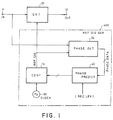
- Fig. 1 is a block diagram to show the first embodiment of this invention digital demodulator.
- Fig. 2 is a block diagram to show the second embodiment of the digital demodulator according to this invention.
- Fig. 3 is a block diagram to show in more detail the first embodiment of this invention digital demodulator.
- Fig. 10 is a block diagram to show the second embodiment of this invention digital decoder in detail.
- Fig. 4 is a chart to explain the operation of the first embodiment of this invention digital demodulator.
- Fig. 5 is a time chart of various signals of the phase difference detection means of the first embodiment of the digital demodulator according to this invention.
- Fig. 6 is a chart to show signal phases in the signal space of a QPSK signal.
- Fig. 7 is a chart to show the phases of a QPSK signal when it is passing a circuit where fading occurs.
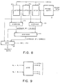
- Fig. 8 is a block diagram to show the reference signal phase prediction means of the first embodiment of this invention digital demodulator.
- Fig. 9 is a block diagram to show an averaging circuit using an adder of the reference signal phase prediction means shown in the first embodiment of this invention digital demodulator.
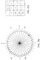
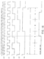
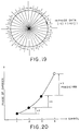
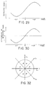
- Fig. 11 are graphs to show the detected phases of a QPSK signal where frequency drift exists between the carrier of the phase modulated signal and the reference signal.
- the phase of the reference signal may be aligned with I or Q axis by detecting the difference and shifting the phase of the reference signal.
- the phase shift will be calculated for setting the phase of the reference signal at either I or Q axis based on the phase difference between the reference signal and a phase modulated signal.
- the calculated phase shift is transmitted to the multiplexer 57 in the reference signal generating means 51 as the reference signal phase prediction data for each decision timing.
- the phase of the reference signal is adjusted again each time by selecting one of the outputs from the shift register 55.
- Figs. 8 and 9 show the reference signal phase prediction means 40 in block diagrams.
- the multiplexer 45 selects the average phase shift of four symbols when the receiving level is low, selects the average phase shift of two symbols when it is medium, and selects the phase shift of one symbol when it is high.
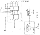
- the reference signal adjusted of its phase and outputted from the reference signal generating means 51 is branched out and is inputted at a clock terminal of the latch circuit 65 of the data generation means for frequency drift compensation 63.
- the output in decimal from the latch circuit 65 is inputted at an adder 67 together with the frequency drift data ⁇ outputted from the frequency drift detection means 61, and the output therefrom is inputted at the latch circuit 65.
- the output in integer from the latch circuit 65 is added to the reference signal phase prediction data outputted from the reference signal phase prediction means 40 by an adder 69, and supplied to a multiplexer 57 of the reference signal control means 51.
- a phase modulated signal inputted at the input 11 is detected by the reference signal of which phase is readjusted by multipliers 26 1 and 26 2 of the detector 20 and by the signal obtained by shifting the phase of said reference signal by ⁇ /2, and outputted to the outputs 13 1 and 13 2 as the detection signal I and detection signal Q respectively.
- the reference numeral 23 denotes a ⁇ /2 shift circuit which shifts the reference signal by ⁇ /2.
- Two reference signals act as detection axes which intersect each other at normal angles just like the recovered carrier in the coherent detection.
- the structure is intended for QPSK signals, but the third embodiment is similarly effective for other coherent detectors.
- the phase modulated signal inputted at the input 11 is branched out and inputted at flip-flops 31 1 through 31 n of the phase difference detection means 30.
- the reference signal which has been adjusted in phase is inputted at a phase shift circuit 33 of the means 30, and the outputs C 1 through C n are supplied as clocks to the flip-flops 31 1 through 31 n .
- the phase difference data from the flip-flops 31 1 through 31 n between the phase modulated signal and the reference signal of which phase has been readjusted are taken in by the phase deviation data conversion means 37.
- the memory 48 of the means 40 stores the reference signal phase prediction data for the decision timing in the next symbol using as an address the data indicating the phase deviations of the carrier in the past m symbols. In other words, if the phase deviations of the carrier are obtained for the past m symbols, the phase of the reference signal (carrier in the case of coherent detection) in the immediately following symbol may be predicted by the memory 48.
- the phase deviation between the first and the second symbols is +2, and that between the second and the third symbols is +4, the phase deviation between the third and the fourth symbols can be predicted as +7. If this prediction is correct, the phase difference in the following symbol between the phase modulated signal and the reference signal of which the phase has been adjusted based on the prediction becomes substantially equal to ⁇ /4 ⁇ i x ⁇ /2 , and the phase deviation data becomes 0. As the phase deviation of the carrier at this time becomes equal to the predicted value (or the reference signal phase prediction data), the value is set at the latch circuit 43 as a new input address.
- Fig. 21 is a block diagram to show the fourth embodiment of this invention digital demodulator.
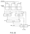
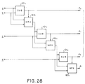
- Fig. 22 is a block diagram to show an averaging circuit of the fourth embodiment digital demodulator.
- the reference signal phase prediction means 40' comprises an averaging circuit 47 which receives as an input the phase deviation data and a selector circuit 49 which selects either one of the output from the averaging circuit 47 or the output from the memory 46 and outputs it as the reference signal phase prediction data.
- the averaging circuit 47 and latch circuit 43 receive as an input the decision timing signals and the averaging circuit 47 and the selector circuit 49 receive as an input the reception level data which indicates the transmission conditions.
- the bit error rate performance comparable to that in the coherent detection is obtained in the low level reception region while the performance superior to that in the coherent or differential detection can be obtained in the high level reception region.
- this system can achieve excellent detection performance (or bit error rate performance) over a wide scope of reception levels.
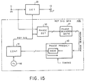
- a frequency drift detection means 100 estimates frequency drift of carrier based on the output from the phase difference distribution detection means 90.
- the circuit is structured as above, based on the coded data [F 0 , F 1 , F 2 ] from the subtractors 101 1 through 101 3 , it becomes possible to detect in which phase region the number of detection becomes maximum.
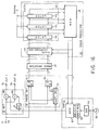
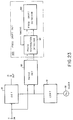
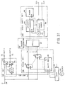
- Fig. 31 is a block diagram to show the sixth embodiment of this invention digital demodulator, and Fig. 32 an explanatory view of the operation of a phase difference decision circuit of the sixth embodiment.
- the direction of the frequency drift may be judged by comparing the time when the phase of the modulated signal stays in the region ⁇ with the time when it stays in the region ⁇ because the two time periods become substantially the same if there is no frequency drift.
- the up-down counter 109 counts upward clocks outputted from the clock generator 107 while the phase of the signal stays in the region ⁇ and counts downward clocks while the phase of the signal stays in the region ⁇ depending on the output from the phase difference processing circuit 97.
- the count detection circuit 109 monitors the number of the counts by the up-down counter 105 and when the number of counts exceeds a predetermined level in either directions, transmits detection pulses to corresponding outputs 111 u and 111 d .
- the direction (either negative or positive) of the frequency drift may be judged from such detection pulses.
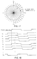
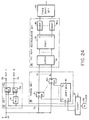
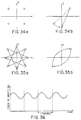
- Fig. 34 is a view to explain the principle of the ⁇ /4 shift QPSK modulation method.
- Fig. 35 is an explanatory view of the preamble generation by the ⁇ /4 shift QPSK modulation method, and
- Fig. 36 is a view to show the changes in frequency of the modulated signals in a short period of time when preamble signals are transmitted.
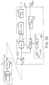
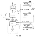
- the frequency of the modulated signals may be measured and converted to the frequency of the reference signal even while the preamble signals for clock recovery of the seventh embodiment are being transmitted, setting of preamble signals otherwise required for the measurement of the frequency of the reference signal is no longer necessary, and transmission efficiency is enhanced.
Landscapes
- Engineering & Computer Science (AREA)
- Computer Networks & Wireless Communication (AREA)
- Signal Processing (AREA)
- Quality & Reliability (AREA)
- Digital Transmission Methods That Use Modulated Carrier Waves (AREA)
Claims (15)
- Générateur de signal de référence destiné à générer un signal de référence afin de démoduler un signal modulé en phase, comprenant :un moyen de commande et d'ajustement de phase (40, 51) destiné à générer le signal de référence à partir d'un signal d'entrée d'horloge, le moyen de commande et d'ajustement de phase (40, 51) étant capable de générer un certain nombre de signaux de sortie différents dont l'un, en fonctionnement, sert de signal de référence provenant du générateur de signal de référence etun moyen de comparaison (30), relié de façon à recevoir le signal de référence et à recevoir le signal modulé en phase, afin de déterminer une relation de phase entre les deux signaux reçus et de fournir un signal de sortie de commande vers le moyen de commande et d'ajustement de phase (40, 51) indiquant la relation de phase,le moyen de commande et d'ajustement de phase (40, 51), en fonctionnement, modifiant le signal de référence, en fournissant, à sa place, un autre signal parmi les plusieurs signaux de sortie différents, si le signal de sortie de commande provenant du moyen de comparaison (30) indique au moyen de commande et d'ajustement de phase (40, 51) que la modification de signal de référence résultera en un déplacement plus proche d'une relation de phase désirée entre le signal de référence et le signal modulé en phase,
caractérisé en ce que le moyen de commande et d'ajustement de phase (40, 51) comprend un moyen de prédiction de phase (40) relié de façon à recevoir le signal de sortie de commande provenant du moyen de comparaison (30) et à fournir un signal de commande au moyen de commande (51), en vue de sélectionner le signal de sortie servant de signal de référence. - Générateur de signal de référence selon la revendication 1, dans lequel le moyen de commande et d'ajustement de phase (40, 51) comprend un moyen de commande (51) capable de générer, à partir du signal d'entrée d'horloge, un certain nombre de signaux d'horloge décalés en phase présentant des déphasages différents par rapport au signal modulé en phase, le moyen de commande et d'ajustement de phase (40, 51) fonctionnant de manière à ce que l'un des signaux d'horloge décalés en phase serve de signal de référence.
- Générateur de signal de référence selon la revendication 1 ou la revendication 2, dans lequel le moyen de comparaison (30) comprend un registre à décalage (33) qui porte le signal de référence en tant que premier mot numérique et un certain nombre de registres (311 à 31n) qui portent le signal modulé en phase en tant que second mot numérique, les plusieurs registres (311 à 31n) étant reliés de façon à être cadencés par le premier mot numérique provenant du registre à décalage (33) et la sortie du moyen de comparaison (30) constituant les sorties combinées des plusieurs registres (311 à 31n) représentant un troisième mot numérique.
- Générateur de signal de référence selon la revendication 3, dans lequel le moyen de commande (51) comprend un second registre à décalage (55) relié de façon à recevoir le signal d'entrée d'horloge sous forme d'une entrée série et à fournir un certain nombre de sorties parallèles à partir de ses étages respectifs, chaque étage du second registre à décalage (55) étant relié à une entrée respective d'un multiplexeur (57) qui est relié de façon à être commandé par le moyen de prédiction de phase (40) et, en fonctionnement, le multiplexeur (57) fournit le signal de référence.
- Générateur de signal de référence selon l'une quelconque des revendications 2 à 4, dans lequel le moyen de prédiction de phase (40) comprend un point d'accès d'entrée de commande destiné à recevoir un signal indicatif du niveau reçu du signal modulé en phase et le signal de commande fourni par le moyen de prédiction de phase (40) dépend du signal qui est présent au niveau du point d'accès d'entrée de commande.
- Générateur de signal de référence selon la revendication 5, dans lequel le moyen de prédiction de phase (40), en fonctionnement, fournit un signal de commande sur la base du signal modulé en phase pendant la durée d'un seul symbole lorsque le signal présent au niveau de son point d'accès d'entrée de commande indique que le signal modulé en phase dépasse un premier niveau de réception.
- Générateur de signal de référence selon la revendication 5 ou la revendication 6, dans lequel le moyen de prédiction de phase (40) fournit un signal de commande sur la base des signaux modulés en phase pendant la durée d'une séquence de symboles, lorsque le signal présent à son point d'accès d'entrée de commande indique que les signaux modulés en phase ne dépassent pas un premier niveau de réception.
- Générateur de signal de référence selon la revendication 7, dans lequel le moyen de prédiction de phase (40) comprend une mémoire (48) et un moyen de circuit à verrouillage associé (43), la mémoire (48) mémorisant les valeurs de phase prédites pour les signaux modulés en phase et le moyen de circuit à verrouillage (43) mémorisant la séquence de symboles sous forme d'adresses pour la mémoire (48).
- Générateur de signal de référence selon l'une quelconque des revendications 5 à 8, dans lequel le moyen de prédiction de phase (40) fournit un signal de commande fixe durant une période quelconque dans lequel le signal présent à son point d'accès d'entrée de commande indique que le signal modulé en phase est situé en dessous d'un second niveau, le second niveau étant inférieur au premier niveau, le signal de commande fixe étant celui fourni à la dernière occasion pour laquelle le signal modulé en phase était au-dessus du second niveau.
- Générateur de signal de référence selon l'une quelconque des revendications 1 à 9, dans lequel le moyen de comparaison (30) comprend un circuit de quantification de phase directe (603) destiné à fournir une sortie sous forme de mots numériques.
- Générateur de signal de référence selon la revendication 1, dans lequel le moyen de commande et d'ajustement de phase comprend :un compteur (223) relié à un point d'accès d'entrée de signal à partir duquel le signal modulé en phase est acheminé vers un moyen de comparaison (231),un générateur de période de temporisation (225, 227) relié au compteur (223) afin de générer une période de temporisation pour le compteur (223),un convertisseur de fréquence de signal de référence (229) relié au compteur (223) afin de convertir la sortie provenant du compteur (223),un générateur de données (233) relié de façon a recevoir et à répondre à la sortie provenant du moyen de comparaison (231) etun générateur de synchronisation (235) relié de façon à recevoir et à répondre à la sortie provenant du générateur de données (233) et à fournir la sortie à partir du générateur de fréquence de référence.
- Générateur de signal de référence selon l'une quelconque des revendications 1 à 11, comprenant un moyen de détection de dérive de fréquence destiné à détecter la dérive de fréquence dans le signal modulé en phase et un moyen relié de façon à modifier le signal de référence conformément à la sortie provenant du moyen de détection de dérive de fréquence.
- Générateur de signal de référence selon la revendication 12, comprenant un moyen de détection de distribution de différence de phase destiné à mémoriser des données de différence de phase sur le signal modulé en phase et un moyen de détection de dérive de fréquence destiné à calculer la dérive de fréquence du signal modulé en phase à partir des données mémorisées.
- Générateur de signal de référence selon la revendication 12 ou 13, comprenant un moyen de limitation destiné à établir une limite de plage pour la compensation de dérive de fréquence.
- Démodulateur numérique comprenant :un générateur de signal de référence selon l'une quelconque des revendications 1 à 14, etun détecteur (20) relié de façon à recevoir le signal modulé en phase à un premier point d'accès d'entrée et à recevoir le signal de référence à un second point d'accès d'entrée afin de fournir un signal détecté de sortie.
Applications Claiming Priority (10)
| Application Number | Priority Date | Filing Date | Title |
|---|---|---|---|
| JP27566289 | 1989-10-23 | ||
| JP27566289 | 1989-10-23 | ||
| JP275662/89 | 1989-10-23 | ||
| JP28006389 | 1989-10-27 | ||
| JP28006389 | 1989-10-27 | ||
| JP280063/89 | 1989-10-27 | ||
| JP1282610A JPH0767117B2 (ja) | 1989-10-30 | 1989-10-30 | ディジタル復調器 |
| JP28261089 | 1989-10-30 | ||
| JP282610/89 | 1989-10-30 | ||
| PCT/JP1990/001350 WO1991006166A1 (fr) | 1989-10-23 | 1990-10-19 | Demodulateur numerique |
Publications (3)
| Publication Number | Publication Date |
|---|---|
| EP0451289A1 EP0451289A1 (fr) | 1991-10-16 |
| EP0451289A4 EP0451289A4 (en) | 1993-05-12 |
| EP0451289B1 true EP0451289B1 (fr) | 2000-07-26 |
Family
ID=27336282
Family Applications (1)
| Application Number | Title | Priority Date | Filing Date |
|---|---|---|---|
| EP90915174A Expired - Lifetime EP0451289B1 (fr) | 1989-10-23 | 1990-10-19 | Générateur de signal de référence et démodulateur numérique le contenant |
Country Status (5)
| Country | Link |
|---|---|
| US (1) | US5260975A (fr) |
| EP (1) | EP0451289B1 (fr) |
| CA (1) | CA2044252C (fr) |
| DE (1) | DE69033596T2 (fr) |
| WO (1) | WO1991006166A1 (fr) |
Cited By (1)
| Publication number | Priority date | Publication date | Assignee | Title |
|---|---|---|---|---|
| DE102004047398B3 (de) * | 2004-09-29 | 2006-02-16 | Infineon Technologies Ag | Gemeinsamer Detektor für Taktphase und Trägerphase |
Families Citing this family (52)
| Publication number | Priority date | Publication date | Assignee | Title |
|---|---|---|---|---|
| DE69232647T2 (de) * | 1991-03-20 | 2002-11-28 | Sony Corp., Tokio/Tokyo | Demodulator zur Demodulierung eines pi/4-umgetasteten DQPSK-Signals |
| GB2260046B (en) * | 1991-09-26 | 1995-02-15 | Northern Telecom Ltd | Optical communications systems |
| KR960014411B1 (ko) * | 1991-12-13 | 1996-10-15 | 모토로라 인코포레이티드 | 직접 위상 계수화 장치 및 방법 |
| US5376894A (en) * | 1992-12-31 | 1994-12-27 | Pacific Communication Sciences, Inc. | Phase estimation and synchronization using a PSK demodulator |
| JPH06205062A (ja) * | 1993-01-08 | 1994-07-22 | Nec Corp | 遅延検波回路 |
| TW234796B (fr) * | 1993-02-24 | 1994-11-21 | Advanced Micro Devices Inc | |
| US5461643A (en) * | 1993-04-08 | 1995-10-24 | Motorola | Direct phase digitizing apparatus and method |
| US5444639A (en) * | 1993-09-07 | 1995-08-22 | Rockwell International Corporation | Angular rate sensing system and method, with digital synthesizer and variable-frequency oscillator |
| US5834950A (en) * | 1994-03-17 | 1998-11-10 | 3Com Corporation | Phase detector which eliminates frequency ripple |
| JPH07321862A (ja) * | 1994-05-25 | 1995-12-08 | Matsushita Electric Ind Co Ltd | ディジタル変調波復調装置 |
| US6023491A (en) * | 1994-06-21 | 2000-02-08 | Matsushita Electric Industrail Co., Ltd. | Demodulation apparatus performing different frequency control functions using separately provided oscillators |
| JP3390272B2 (ja) * | 1994-11-10 | 2003-03-24 | 沖電気工業株式会社 | 同期検波回路 |
| JP3118384B2 (ja) * | 1994-12-05 | 2000-12-18 | 株式会社ケンウッド | 受信信号変調方式識別回路 |
| US5590140A (en) * | 1994-12-30 | 1996-12-31 | Lucent Technologies Inc. | Clock recovery extrapolation |
| JPH0983588A (ja) * | 1995-09-18 | 1997-03-28 | Mitsubishi Electric Corp | 復調器及び変復調システム及び復調方法 |
| JP3575883B2 (ja) * | 1995-09-18 | 2004-10-13 | 三菱電機株式会社 | ディジタル復調器 |
| US5663666A (en) * | 1996-02-21 | 1997-09-02 | Hewlett-Packard Company | Digital phase detector |
| US5710732A (en) * | 1996-04-22 | 1998-01-20 | Samsung Electronics Co., Ltd. | Calculating the average of four integer numbers rounded away from zero in a single instruction cycle |
| US5751617A (en) * | 1996-04-22 | 1998-05-12 | Samsung Electronics Co., Ltd. | Calculating the average of two integer numbers rounded away from zero in a single instruction cycle |
| EP0820173A3 (fr) * | 1996-07-16 | 2001-01-24 | Matsushita Electric Industrial Co., Ltd. | Récepteur MAQ, à compensation d'erreur en phase et en fréquence en bande de base |
| US5917739A (en) * | 1996-11-14 | 1999-06-29 | Samsung Electronics Co., Ltd. | Calculating the average of four integer numbers rounded towards zero in a single instruction cycle |
| US6007232A (en) * | 1996-11-14 | 1999-12-28 | Samsung Electronics Co., Ltd. | Calculating the average of two integer numbers rounded towards zero in a single instruction cycle |
| DE19732894C2 (de) * | 1997-07-30 | 1999-11-11 | Siemens Ag | Verfahren und Anordnungen zum schnellen Synchronisieren zweier Trägersignale |
| JP3504470B2 (ja) * | 1997-09-18 | 2004-03-08 | 日本放送協会 | Afc回路、キャリア再生回路および受信装置 |
| JPH11284677A (ja) * | 1998-03-27 | 1999-10-15 | Nec Corp | 復調器とこれを用いたディジタル無線通信システム |
| US6163208A (en) * | 1998-12-15 | 2000-12-19 | Ga-Tek Inc. | One bit digital phase shift keyed carrier recovery and demodulator circuit |
| WO2000041373A1 (fr) * | 1999-01-06 | 2000-07-13 | Koninklijke Philips Electronics N.V. | Demodulateur a dispositif de rotation pour correction de decalage de frequence |
| GB9901965D0 (en) * | 1999-01-29 | 1999-03-17 | Geo Sensor Corp | Angle demodulation |
| JP2001016284A (ja) * | 1999-07-01 | 2001-01-19 | Nec Saitama Ltd | 移動機用復調装置および移動機用復調方法 |
| US6925136B1 (en) * | 2001-08-29 | 2005-08-02 | The United States Of America As Represented By The Secretary Of The Navy | Simultaneous frequency and phase synchronizer |
| US7184506B2 (en) * | 2002-03-30 | 2007-02-27 | Broadcom Corporation | Frequency drift and phase error compensation in a VOFDM receiver |
| US7215705B2 (en) * | 2003-03-17 | 2007-05-08 | Intel Corporation | Reducing phase noise in phase-encoded communications signals |
| US7512188B1 (en) * | 2003-04-10 | 2009-03-31 | Xilinx, Inc. | Phase shift keying signaling for integrated circuits |
| US7328230B2 (en) * | 2004-03-26 | 2008-02-05 | Intel Corporation | SIMD four-data element average instruction |
| US7412473B2 (en) * | 2004-09-01 | 2008-08-12 | Ceva D.S.P. Ltd. | Arithmetic circuitry for averaging and methods thereof |
| US7764741B2 (en) * | 2005-07-28 | 2010-07-27 | Broadcom Corporation | Modulation-type discrimination in a wireless communication network |
| US7747177B2 (en) | 2005-08-15 | 2010-06-29 | Alcatel-Lucent Usa Inc. | Coherent phase-shift-keying |
| DE102005041455A1 (de) * | 2005-08-31 | 2007-03-15 | Abb Patent Gmbh | Automatisierungstechnische Einrichtung |
| DE102005043485A1 (de) | 2005-09-13 | 2007-03-15 | Abb Patent Gmbh | Automatisierungstechnische Einrichtung |
| DE102005043478A1 (de) * | 2005-09-13 | 2007-03-15 | Abb Patent Gmbh | Automatisierungstechnische Einrichtung |
| DE102005043481A1 (de) * | 2005-09-13 | 2007-03-15 | Abb Patent Gmbh | Automatisierungstechnische Einrichtung |
| DE102005043482A1 (de) * | 2005-09-13 | 2007-03-15 | Abb Patent Gmbh | Automatisierungstechnische Einrichtung |
| US7764886B2 (en) | 2005-11-28 | 2010-07-27 | Alcatel Lucent | Burst mode optical receiver |
| US7865088B2 (en) | 2006-05-12 | 2011-01-04 | Alcatel Lucent | Burst mode optical receiver |
| US7929866B2 (en) * | 2005-11-28 | 2011-04-19 | Alcatel Lucent | Passive optical network media access controller assisted clock recovery |
| US7711273B2 (en) | 2006-03-03 | 2010-05-04 | Alcatel-Lucent Usa Inc. | Optical quadrature-amplitude modulation receiver |
| US7688918B2 (en) | 2006-07-07 | 2010-03-30 | Alcatel-Lucent Usa Inc. | Recursive phase estimation for a phase-shift-keying receiver |
| US8044742B2 (en) * | 2009-03-11 | 2011-10-25 | Qualcomm Incorporated | Wideband phase modulator |
| RU2577192C1 (ru) * | 2015-02-11 | 2016-03-10 | Межрегиональное общественное учреждение "Институт инженерной физики" | Некогерентный демодулятор бинарного цифрового сигнала с мягким итеративным декодированием данных |
| TWI682387B (zh) * | 2018-10-24 | 2020-01-11 | 新唐科技股份有限公司 | 多音調通訊系統、多音調訊號解調變裝置及其方法 |
| US11381430B2 (en) * | 2020-03-19 | 2022-07-05 | Cypress Semiconductor Corporation | Phase/frequency tracking transceiver |
| DE102021211337A1 (de) * | 2021-10-07 | 2023-04-13 | Continental Automotive Technologies GmbH | Verfahren zur Offset-Kompensation von Sensorsignalen, Offsetkompensationsvorrichtung und Sensorvorrichtung |
Family Cites Families (8)
| Publication number | Priority date | Publication date | Assignee | Title |
|---|---|---|---|---|
| JPS5535545A (en) * | 1978-09-04 | 1980-03-12 | Nec Corp | Digital phase synchronous circuit |
| US4308505A (en) * | 1979-06-13 | 1981-12-29 | Trw, Inc. | Frequency detector device and method |
| CA1246707A (fr) * | 1984-02-20 | 1988-12-13 | Botaro Hirosaki | Dispositif pour supprimer les fluctuations de phase periodiques dans une porteuse |
| DE3443924A1 (de) * | 1984-12-01 | 1986-06-05 | Philips Patentverwaltung Gmbh, 2000 Hamburg | Schaltungsanordnung zum ableiten eines stellsignals |
| JPH01115250A (ja) * | 1987-10-29 | 1989-05-08 | Yagi Antenna Co Ltd | 復調搬送波生成方式 |
| JPH01117451A (ja) * | 1987-10-30 | 1989-05-10 | Nec Corp | 復調回路 |
| JPH01228355A (ja) * | 1988-03-09 | 1989-09-12 | Nippon Telegr & Teleph Corp <Ntt> | 同期検波器 |
| JPH0787476B2 (ja) * | 1988-10-07 | 1995-09-20 | 日本電気株式会社 | 復調装置 |
-
1990
- 1990-10-19 CA CA002044252A patent/CA2044252C/fr not_active Expired - Lifetime
- 1990-10-19 US US07/720,505 patent/US5260975A/en not_active Expired - Lifetime
- 1990-10-19 WO PCT/JP1990/001350 patent/WO1991006166A1/fr not_active Ceased
- 1990-10-19 DE DE69033596T patent/DE69033596T2/de not_active Expired - Lifetime
- 1990-10-19 EP EP90915174A patent/EP0451289B1/fr not_active Expired - Lifetime
Non-Patent Citations (2)
| Title |
|---|
| Patent Abstracts of Japan vol. 4, no. 67 (E-011) , 20 May 1980 & JP 55 035545 A (NEC corp.), 12 March 1980 * |
| Patent Abstracts of Japan vol. 4, no. 67 (E-011), 20 May 1980 & JP 55 035545 A (NEC corp.), 12 March 1980 * |
Cited By (1)
| Publication number | Priority date | Publication date | Assignee | Title |
|---|---|---|---|---|
| DE102004047398B3 (de) * | 2004-09-29 | 2006-02-16 | Infineon Technologies Ag | Gemeinsamer Detektor für Taktphase und Trägerphase |
Also Published As
| Publication number | Publication date |
|---|---|
| US5260975A (en) | 1993-11-09 |
| WO1991006166A1 (fr) | 1991-05-02 |
| DE69033596T2 (de) | 2001-04-19 |
| CA2044252A1 (fr) | 1991-04-24 |
| CA2044252C (fr) | 1999-08-17 |
| EP0451289A4 (en) | 1993-05-12 |
| EP0451289A1 (fr) | 1991-10-16 |
| DE69033596D1 (de) | 2000-08-31 |
Similar Documents
| Publication | Publication Date | Title |
|---|---|---|
| US5260975A (en) | Digital demodulator | |
| US5574399A (en) | Coherent PSK detector not requiring carrier recovery | |
| US5097220A (en) | Circuit for demodulating psk modulated signal by differential-defection | |
| US6104762A (en) | Timing recovery apparatus and a diversity communication apparatus using the same | |
| EP0464814B1 (fr) | Circuit de démodulation de signaux modulés en PSK | |
| EP0504890B1 (fr) | Démodulateur pour démoduler un signal modulé différentiellement en quadrature de phase avec déphasage de pi/4 | |
| EP0848523A2 (fr) | Démodulateur de signaux MDP, employant l'algorithme CORDIC | |
| EP0940957B1 (fr) | Circuit de réglage automatique de fréquence (RAF), circuit reproducteur de porteuses, et récepteur | |
| EP0637883B1 (fr) | Circuit de récupération de porteuse pour démodulateurs de signaux modulés en quadrature décalée | |
| US5497400A (en) | Decision feedback demodulator with phase and frequency estimation | |
| JPS62222745A (ja) | 復調装置 | |
| US6081563A (en) | AFC circuit of digital demodulation device | |
| US4334312A (en) | Phase synchronizing circuit for use in multi-level, multi-phase, superposition-modulated signal transmission system | |
| JP2000049882A (ja) | クロック同期回路 | |
| EP1039709B1 (fr) | Récepteur pour des signaux modulés par une pluralité de schémas de modulation PSK | |
| US6411658B1 (en) | Demodulation device | |
| JP2903104B2 (ja) | ディジタル移動無線通信方式 | |
| US7092458B2 (en) | Carrier recovery circuit and lock detection circuit for mixed PSK signals | |
| EP1052818B1 (fr) | Récepteur | |
| US4498050A (en) | Demodulation device for composite PSK-PSK modulated waves | |
| JP3865893B2 (ja) | 復調回路 | |
| JPH10229423A (ja) | タイミング再生回路及びこれを用いた復調器 | |
| JPH03205940A (ja) | ディジタル復調器 | |
| EP0592978B1 (fr) | Stabilisateur de fréquence dans un système de radio-communications à signaux modulés en phase | |
| JPH0767117B2 (ja) | ディジタル復調器 |
Legal Events
| Date | Code | Title | Description |
|---|---|---|---|
| PUAI | Public reference made under article 153(3) epc to a published international application that has entered the european phase |
Free format text: ORIGINAL CODE: 0009012 |
|
| AK | Designated contracting states |
Kind code of ref document: A1 Designated state(s): DE FR GB SE |
|
| 17P | Request for examination filed |
Effective date: 19911022 |
|
| A4 | Supplementary search report drawn up and despatched |
Effective date: 19930323 |
|
| AK | Designated contracting states |
Kind code of ref document: A4 Designated state(s): DE FR GB SE |
|
| 17Q | First examination report despatched |
Effective date: 19970210 |
|
| GRAG | Despatch of communication of intention to grant |
Free format text: ORIGINAL CODE: EPIDOS AGRA |
|
| RTI1 | Title (correction) |
Free format text: REFERENCE SIGNAL GENERATOR AND DIGITAL DEMODULATOR INCLUDING THE SAME |
|
| RTI1 | Title (correction) |
Free format text: REFERENCE SIGNAL GENERATOR AND DIGITAL DEMODULATOR INCLUDING THE SAME |
|
| GRAG | Despatch of communication of intention to grant |
Free format text: ORIGINAL CODE: EPIDOS AGRA |
|
| GRAH | Despatch of communication of intention to grant a patent |
Free format text: ORIGINAL CODE: EPIDOS IGRA |
|
| RAP1 | Party data changed (applicant data changed or rights of an application transferred) |
Owner name: NIPPON TELEGRAPH AND TELEPHONE CORPORATION Owner name: NTT MOBILE COMMUNICATIONS NETWORK INC. |
|
| GRAH | Despatch of communication of intention to grant a patent |
Free format text: ORIGINAL CODE: EPIDOS IGRA |
|
| RAP1 | Party data changed (applicant data changed or rights of an application transferred) |
Owner name: NTT MOBILE COMMUNICATIONS NETWORK INC. Owner name: NIPPON TELEGRAPH AND TELEPHONE CORPORATION |
|
| GRAA | (expected) grant |
Free format text: ORIGINAL CODE: 0009210 |
|
| AK | Designated contracting states |
Kind code of ref document: B1 Designated state(s): DE FR GB SE |
|
| REF | Corresponds to: |
Ref document number: 69033596 Country of ref document: DE Date of ref document: 20000831 |
|
| ET | Fr: translation filed | ||
| PLBE | No opposition filed within time limit |
Free format text: ORIGINAL CODE: 0009261 |
|
| STAA | Information on the status of an ep patent application or granted ep patent |
Free format text: STATUS: NO OPPOSITION FILED WITHIN TIME LIMIT |
|
| 26N | No opposition filed | ||
| REG | Reference to a national code |
Ref country code: GB Ref legal event code: IF02 |
|
| PGFP | Annual fee paid to national office [announced via postgrant information from national office to epo] |
Ref country code: DE Payment date: 20091015 Year of fee payment: 20 Ref country code: SE Payment date: 20091007 Year of fee payment: 20 |
|
| PGFP | Annual fee paid to national office [announced via postgrant information from national office to epo] |
Ref country code: GB Payment date: 20091014 Year of fee payment: 20 Ref country code: FR Payment date: 20091029 Year of fee payment: 20 |
|
| REG | Reference to a national code |
Ref country code: GB Ref legal event code: PE20 Expiry date: 20101018 |
|
| EUG | Se: european patent has lapsed | ||
| PG25 | Lapsed in a contracting state [announced via postgrant information from national office to epo] |
Ref country code: GB Free format text: LAPSE BECAUSE OF EXPIRATION OF PROTECTION Effective date: 20101018 |
|
| PG25 | Lapsed in a contracting state [announced via postgrant information from national office to epo] |
Ref country code: DE Free format text: LAPSE BECAUSE OF EXPIRATION OF PROTECTION Effective date: 20101019 |