EP0452825A2 - Procédé et appareil pour la correction de fond lors de l'analyse de la surface d'un spécimen - Google Patents
Procédé et appareil pour la correction de fond lors de l'analyse de la surface d'un spécimen Download PDFInfo
- Publication number
- EP0452825A2 EP0452825A2 EP91105876A EP91105876A EP0452825A2 EP 0452825 A2 EP0452825 A2 EP 0452825A2 EP 91105876 A EP91105876 A EP 91105876A EP 91105876 A EP91105876 A EP 91105876A EP 0452825 A2 EP0452825 A2 EP 0452825A2
- Authority
- EP
- European Patent Office
- Prior art keywords
- specimen
- surface area
- background
- distribution data
- predetermined
- Prior art date
- Legal status (The legal status is an assumption and is not a legal conclusion. Google has not performed a legal analysis and makes no representation as to the accuracy of the status listed.)
- Granted
Links
- 238000000034 method Methods 0.000 title claims abstract description 19
- 238000003705 background correction Methods 0.000 title claims abstract description 16
- 238000004458 analytical method Methods 0.000 title claims abstract description 12
- 238000009826 distribution Methods 0.000 claims abstract description 50
- 238000010894 electron beam technology Methods 0.000 claims abstract description 32
- 230000001678 irradiating effect Effects 0.000 claims description 9
- 238000004020 luminiscence type Methods 0.000 claims description 4
- 230000015654 memory Effects 0.000 description 10
- 239000013078 crystal Substances 0.000 description 6
- 238000005259 measurement Methods 0.000 description 6
- 239000000523 sample Substances 0.000 description 4
- 230000000875 corresponding effect Effects 0.000 description 3
- 238000006243 chemical reaction Methods 0.000 description 2
- 230000002596 correlated effect Effects 0.000 description 2
- 230000002411 adverse Effects 0.000 description 1
- 230000015572 biosynthetic process Effects 0.000 description 1
- 230000001276 controlling effect Effects 0.000 description 1
- 238000012937 correction Methods 0.000 description 1
- 230000007547 defect Effects 0.000 description 1
- 238000001514 detection method Methods 0.000 description 1
- 238000010586 diagram Methods 0.000 description 1
- 230000005284 excitation Effects 0.000 description 1
- 238000004519 manufacturing process Methods 0.000 description 1
- 238000013507 mapping Methods 0.000 description 1
- 238000004452 microanalysis Methods 0.000 description 1
- 238000012545 processing Methods 0.000 description 1
- 238000005211 surface analysis Methods 0.000 description 1
Images

Classifications
-
- H—ELECTRICITY
- H01—ELECTRIC ELEMENTS
- H01J—ELECTRIC DISCHARGE TUBES OR DISCHARGE LAMPS
- H01J37/00—Discharge tubes with provision for introducing objects or material to be exposed to the discharge, e.g. for the purpose of examination or processing thereof
- H01J37/252—Tubes for spot-analysing by electron or ion beams; Microanalysers
- H01J37/256—Tubes for spot-analysing by electron or ion beams; Microanalysers using scanning beams
-
- G—PHYSICS
- G01—MEASURING; TESTING
- G01N—INVESTIGATING OR ANALYSING MATERIALS BY DETERMINING THEIR CHEMICAL OR PHYSICAL PROPERTIES
- G01N23/00—Investigating or analysing materials by the use of wave or particle radiation, e.g. X-rays or neutrons, not covered by groups G01N3/00 – G01N17/00, G01N21/00 or G01N22/00
- G01N23/22—Investigating or analysing materials by the use of wave or particle radiation, e.g. X-rays or neutrons, not covered by groups G01N3/00 – G01N17/00, G01N21/00 or G01N22/00 by measuring secondary emission from the material
- G01N23/225—Investigating or analysing materials by the use of wave or particle radiation, e.g. X-rays or neutrons, not covered by groups G01N3/00 – G01N17/00, G01N21/00 or G01N22/00 by measuring secondary emission from the material using electron or ion
- G01N23/2251—Investigating or analysing materials by the use of wave or particle radiation, e.g. X-rays or neutrons, not covered by groups G01N3/00 – G01N17/00, G01N21/00 or G01N22/00 by measuring secondary emission from the material using electron or ion using incident electron beams, e.g. scanning electron microscopy [SEM]
- G01N23/2252—Measuring emitted X-rays, e.g. electron probe microanalysis [EPMA]
Definitions
- This invention relates to a method and apparatus for analyzing the surface of a specimen such as an electron probe microanalyzer (EPMA), a scanning electron microscope (SEM) and the like, and more particularly to background correction of the measured data in such surface microanalyzers.
- EPMA electron probe microanalyzer
- SEM scanning electron microscope
- the surface of a specimen to be analyzed is scanned by an electron beam having a diameter of several ten angstroms, so that the various kinds of information emerging from each and every minute points on the specimen surface scanned by the electron beam are electrically detected, and displayed in terms of composition of the specimen and/or concentration of the components thereof on a cathode-ray tube in synchronism with the scanning of the specimen surface thereby to display the distribution of the elements contained in the specimen.
- the peaks of the characteristic X rays emitted by the component elements of the specimen under examination are superimposed on a background caused by the inherent characteristic of the instrument, the conditions of excitation of the specimen and the composition of the specimen. This means that the measured data of the distribution of the elements in the specimen contain errors caused by background. Therefore, it is customary to correct the measured data for the background.
- Japanese Unexamined Patent Publication No. 2-10639 discloses a third method of background correction which uses two X-ray spectrometers for each element to be analyzed.
- the focal points of the two X-ray spectrometers are so set as to coincide on the surface of a specimen to be analyzed, and one of the spectrometers is set to an X-ray wavelength characteristic of an element to be measured contained in the specimen while the other spectrometer is set to a wavelength adjacent to the base of the above-mentioned characterisitc X-ray peak wavelength of the element to be measured, and the specimen surface is scanned by both spectrometers simultaneously thereby to obtain both the characteristic X-ray data of the element being measured containing background and the background data at the same time for backgrond correction of the measured data of the specimen.
- the specimen surface is scanned twice, so that a long time is required for analysis of the specimen surface.
- the time required for measurement is advantageously shorter than in the first method.
- Background is caused by not only the characteristic of the instrument and the exciting conditions of the specimen but also the composition of the elements present at the measured spots on the specimen surface, so that accurate background correction cannot be effected.
- the third method which uses two X-ray spectrometers for each element to be analyzed has solved the problems involved in the time required for analysis and adverse influences by the elemental composition at the measured spots of the specimen surface.
- two X-ray spectrometers are required for each element to be measured, so that the whole apparatus becomes bulky with an increased manufacturing cost.
- this invention provides a method and apparatus for analyzing the surface of a specimen which is capable of making an accurate background correction without increasing the equipment and the time required for analysis.
- the electron probe microanalyzer or the scanning electron microscope is provided with a detector for detecting specimen current the value of which is correlated with the average atomic number of the elements contained in the specimen. Also, the value of background in the measured data of characteristic X rays, Auger electrons, etc. is correlated with the average atomic number. Therefore, if the specimen current and the background intensity of a specimen to be analyzed are measured under the same condition as that under which the distribution data of an element in the specimen is measured and an expression of the relation between the specimen current and the background intensity is formulated, it is possible to correct the measured distribution data of the element for background by the specimen current value by using the expression of the above relation.
- the invention provides a method of background correction of the measured data in microanalysis of the surface of a specimen by irradiating a predetermined area of the specimen surface with an electron beam and detecting a signal caused by the irradiation to occur from an element to be analyzed in the specimen so as to obtain a two-dimensional distribution data of the level of the signal in the irradiated specimen surface area, comprising: detecting a specimen current induced in the specimen by the irradiation of the specimen with the electron beam to obtain a two-dimensional distribution data of the value of the specimen current in the irradiated specimen surface area; measuring the intensity of background and the value of the specimen current on at least one point in the predetermined specimen surface area; formulating a relation between the background intensity and specimen current of the specimen from the measured background intensity and specimen current value on the one point in the specimen surface area; calculating a two-dimensional distribution data of the background intensity from the two-dimensional distribution data of the specimen current value by using the formulated relation; and subtracting the calculated two-dimensional distribution data
- the invention also provides an apparatus for analyzing the surface of a specimen, comprising: means for producing an electron beam; means for irradiating a predetermined area of the specimen surface with the electron beam; first detecting means for detecting a signal caused by the irradiation to occur from the specimen so as to produce a first corresponding output signal; second detecting means for detecting a specimen current induced in the specimen by the irradiation so as to produce a second corresponding output signal; means for storing the first and second output signals; means for correcting the first output signal for background; and means for controlling the irradiating means, storing means and background correcting means so as to formulate a relation between the background intensity and specimen current of the specimen from the first and second output signals detected on at least one point in the predetermined specimen surface area, calculate a distribution data of the background intensity in the predetermined specimen surface area from the distribution data of the specimen current contained in the second output signal detected in the predetermined specimen surface area by using the formulated relation, and subtract the calculated distribution data of the background intensity from the
- FIG. 1 schematically shows one embodiment of the invention in the form of an X-ray spectrometric analyzer which uses an electron probe microanalyzer.
- this type of apparatus is provided with two to six spectrometers arranged about an electron optics for providing an electron beam to irradiate a specimen to be analyzed.
- an electron source 1 produces an electron beam e to irradiate a specimen S to be analyzed.
- the specimen S is supported on a stage 2 which is movable in X- and Y-directions.
- the electron beam e irradiating the specimen S excites emission of X rays, which are directed to an X-ray spectrometer 3 comprising a crystal C having a curved surface, an X-ray detector 4 having a front slit 4 ', and means for connecting the crystal C and the X-ray detector 4 so that the crystal C and the front slit 4' of the X-ray detector 4 and the point on the specimen surface on which the electron beam e impinges are positioned on the circumference of a Rowland circle R , with the focal point of the X-ray spectrometer 3 coinciding with the point on the specimen surface on which the electron beam e impinges.
- a specimen current detector 5 is provided to detect a specimen current induced in the specimen S by the electrons impinging thereon.
- a data writing device 6 is connected to the X-ray detector 4 and the specimen current detector 5. The device 6 performs an analog-to-digital conversion of the outputs from the detectors 4 and 5 and sends the data obtained by the conversion together with the information about the position of the specimen under examination to image memories 7 and 8, respectively, to be stored therein.
- a specimen stage driving device 9 drives the specimen stage 2 in X- and Y-directions by means of a pulse motor not shown.
- a background correcting device 10 conducts necessary operations on the data taken out of the memories 7 and 8 to provide background-corrected data for mapping the distribution of the element in the specimen surface being analyzed. The data is stored in an image memory 11 and displayed on a color cathode-ray tube 12.
- a spectrometer driving device 13 sets the crystal C and the X-ray detector 4 to a position corresponding to a wavelength set by a wavelength setting device 14.
- a central processing unit 15 controls the above-mentioned and other necessary operations of the above-mentioned devices.
- the specimen stage driving device 9 is operated to move the specimen stage 2 so that the electron beam e is incident on a point A (Fig. 3(a)) on the specimen surface where scanning is to be started.
- the spectrometer driving device 13 is operated by the wavelength setting device 14 to set the crystal C to a wavelength at the base of an appropriate one of the characteristic X-ray peaks of an element to be analyzed.
- the specimen S is irradiated with the electron beam e , and the outputs from the X-ray detector 4 and the specimen current detector 5 are written by the data writing device 6 into the image memories 7 and 8, respectively.
- the outputs from the detectors 4 and 5 represent the background intensity and the specimen current, respectively, detected at the point A on the specimen surface.
- the spectrometer driving device 13 is operated by the wavelength setting device 14 to set the crystal C to the appropriate characteristic X-ray peak wavelength of the element to be analyzed.
- the outputs from the X-ray detector 4 and the specimen current detector 5 are applied through the data writing device 6 to the image memories 7 and 8 to be stored therein, respectively.
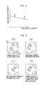
- the output from the X-ray detector 4 stored in the image memory 7 contains a two-dimensional distribution data of the characteristic X-ray peak of the element to be analyzed as shown in Fig. 3(a), and the output from the specimen current detector 5 stored in the image memory 8 contains a two dimensional distribution data of the specimen current as shown in Fig. 3(b).
- the spectrtometer driving device 13 is again operated by the wavelength setting device 14 to set the spectrometer 3 to the wavelength at the base of the appropriate characteristic X-ray peak of the element being analyzed, and the intensity of the background and the value of the specimen current at the point B are measured.
- the results of the measurement are stored in the memories 7 and 8, respectively.
- the background correcting device 10 forms from the background intensity and the specimen current value measured at the two points A and B on the specimen surface a graph of a relation between the background intensity and the specimen current as shown in Fig. 2. Using the relation of the graph shown in Fig.
- the device 10 calculates a two-dimensional distribution data of the background intensity as shown in Fig. 3(c) from the two-dimensional distribution data of the specimen current shown in Fig. 3(b). Then, the background intensity distribution data (Fig. 3(c)) is subtracted from the characteristic X-ray peak data (Fig. 3(a)) of the element being analyzed which is stored in the image memory 7 thereby to obtain a background-corrected, true distribution data of the characteristic X-ray peak of the element as shown in Fig. 3(d). The data is stored in an image memory 11 and displayed on the cathode-ray tube 12.
- the CPU 15 controls the above operations.
- the background intensity and the specimen current are measured at both the starting and finishing points of analysis on the specimen.
- the measurement may also be made on any other points on the specimen.
- Background correction may also be made by detecting the background intensity and the specimen current at any single point on the specimen provided that the relation between the background intensity and the specimen current is known.
- the characteristic X rays are detected to provide a detection signal. It is also possible to detect secondary electrons, reflected electrons, luminescence, Auger electrons, etc. for the same purpose.
- the specimen stage is moved to scan the specimen with the electron beam. It is possible to scan the electron beam over the specimen surface.
- background correction is conducted by utlizing the specimen current detector with which conventional electron probe microanalyzers and scanning electron microscopes are usually provided, it is not necessary to add to the existing equipment any particular device for background correction. Since the measured data of the whole specimen surface to be analyzed can be accurately corrected for background by measuring background at only one or two points on the specimen surface, the time required for analysis can be greatly shortened.
Landscapes
- Chemical & Material Sciences (AREA)
- Analytical Chemistry (AREA)
- Physics & Mathematics (AREA)
- Health & Medical Sciences (AREA)
- Life Sciences & Earth Sciences (AREA)
- Biochemistry (AREA)
- General Health & Medical Sciences (AREA)
- General Physics & Mathematics (AREA)
- Immunology (AREA)
- Pathology (AREA)
- Analysing Materials By The Use Of Radiation (AREA)
Applications Claiming Priority (2)
| Application Number | Priority Date | Filing Date | Title |
|---|---|---|---|
| JP2103363A JPH07119716B2 (ja) | 1990-04-19 | 1990-04-19 | 表面分析装置 |
| JP103363/90 | 1990-04-19 |
Publications (3)
| Publication Number | Publication Date |
|---|---|
| EP0452825A2 true EP0452825A2 (fr) | 1991-10-23 |
| EP0452825A3 EP0452825A3 (en) | 1993-09-01 |
| EP0452825B1 EP0452825B1 (fr) | 1996-11-20 |
Family
ID=14352046
Family Applications (1)
| Application Number | Title | Priority Date | Filing Date |
|---|---|---|---|
| EP91105876A Expired - Lifetime EP0452825B1 (fr) | 1990-04-19 | 1991-04-12 | Procédé et appareil pour la correction de fond lors de l'analyse de la surface d'un spécimen |
Country Status (6)
| Country | Link |
|---|---|
| US (1) | US5128545A (fr) |
| EP (1) | EP0452825B1 (fr) |
| JP (1) | JPH07119716B2 (fr) |
| KR (1) | KR960012331B1 (fr) |
| CN (1) | CN1040251C (fr) |
| DE (1) | DE69123166T2 (fr) |
Cited By (1)
| Publication number | Priority date | Publication date | Assignee | Title |
|---|---|---|---|---|
| US6476389B1 (en) | 1999-03-25 | 2002-11-05 | Fuji Photo Optical Co., Ltd. | X-ray analyzer having an absorption current calculating section |
Families Citing this family (10)
| Publication number | Priority date | Publication date | Assignee | Title |
|---|---|---|---|---|
| US5404110A (en) * | 1993-03-25 | 1995-04-04 | International Business Machines Corporation | System using induced current for contactless testing of wiring networks |
| JP2954819B2 (ja) * | 1993-10-07 | 1999-09-27 | 株式会社東芝 | 全反射蛍光x線分析装置の校正方法 |
| US5656812A (en) * | 1995-07-21 | 1997-08-12 | Jeol Ltd. | Electron probe microanalyzer and X-ray analysis using same |
| US6118123A (en) * | 1997-02-05 | 2000-09-12 | Jeol Ltd. | Electron probe microanalyzer |
| KR100272098B1 (ko) * | 1997-07-16 | 2001-03-02 | 윤종용 | 광디스크재생장치의슬레드편차에따른슬레드모터의구동전압제어방법 |
| JP5039971B2 (ja) * | 2007-01-25 | 2012-10-03 | 国立大学法人東北大学 | 非走査型波長分散型x線分析装置及びそれを用いた測定方法 |
| JP5938708B2 (ja) * | 2011-10-17 | 2016-06-22 | 株式会社リガク | 蛍光x線分析用の較正試料ならびにそれを備える蛍光x線分析装置およびそれを用いる蛍光x線分析方法 |
| CN102765503B (zh) * | 2012-07-26 | 2013-12-18 | 武汉钢铁(集团)公司 | 彩涂钢卷连续在线贴膜及卷取工艺 |
| US11054375B2 (en) | 2016-09-15 | 2021-07-06 | University Of Washington | X-ray spectrometer and methods for use |
| CN107091622B (zh) * | 2017-06-24 | 2020-01-10 | 福建省南安市清信石材有限公司 | 一种纳米分辨率的应变测试设备及方法 |
Family Cites Families (10)
| Publication number | Priority date | Publication date | Assignee | Title |
|---|---|---|---|---|
| JPS5481075A (en) * | 1977-11-24 | 1979-06-28 | Cho Lsi Gijutsu Kenkyu Kumiai | Method of detecting article image using electron beam |
| SU1250925A1 (ru) * | 1984-05-11 | 1986-08-15 | Иркутский государственный университет им.А.А.Жданова | Способ рентгеноспектрального флуоресцентного анализа сплавов |
| SU1224688A1 (ru) * | 1984-07-20 | 1986-04-15 | Казанский Ордена Трудового Красного Знамени Государственный Университет Им.С.М.Кирова | Способ определени фона в рентгенофлуоресцентном анализе сложных по составу сред |
| EP0196804B1 (fr) * | 1985-03-11 | 1991-01-23 | Nippon Telegraph And Telephone Corporation | Méthode et appareil pour tester un dispositif électronique intégré |
| EP0204855B1 (fr) * | 1985-06-11 | 1992-03-04 | Shimadzu Corporation | Méthode et appareil pour l'analyse d'état |
| US4697080A (en) * | 1986-01-06 | 1987-09-29 | The United States Of America As Represented By The United States Department Of Energy | Analysis with electron microscope of multielement samples using pure element standards |
| JPS6385860U (fr) * | 1986-11-26 | 1988-06-04 | ||
| JPS63313043A (ja) * | 1987-06-15 | 1988-12-21 | Jeol Ltd | 平均原子番号によるバックグラウンド推定法 |
| CN1012704B (zh) * | 1988-05-16 | 1991-05-29 | 中国科学院长春光学精密机械研究所 | 双通道比率记录中的串扰补偿方法及装置 |
| JP2842879B2 (ja) * | 1989-01-06 | 1999-01-06 | 株式会社日立製作所 | 表面分析方法および装置 |
-
1990
- 1990-04-19 JP JP2103363A patent/JPH07119716B2/ja not_active Expired - Fee Related
-
1991
- 1991-04-04 US US07/680,427 patent/US5128545A/en not_active Expired - Fee Related
- 1991-04-12 DE DE69123166T patent/DE69123166T2/de not_active Expired - Fee Related
- 1991-04-12 EP EP91105876A patent/EP0452825B1/fr not_active Expired - Lifetime
- 1991-04-13 CN CN91102529A patent/CN1040251C/zh not_active Expired - Fee Related
- 1991-04-15 KR KR1019910006030A patent/KR960012331B1/ko not_active Expired - Fee Related
Cited By (2)
| Publication number | Priority date | Publication date | Assignee | Title |
|---|---|---|---|---|
| US6476389B1 (en) | 1999-03-25 | 2002-11-05 | Fuji Photo Optical Co., Ltd. | X-ray analyzer having an absorption current calculating section |
| GB2348288B (en) * | 1999-03-25 | 2003-10-01 | Fuji Photo Optical Co Ltd | X-ray analyzer and analyzing method using the same |
Also Published As
| Publication number | Publication date |
|---|---|
| KR960012331B1 (ko) | 1996-09-18 |
| JPH042955A (ja) | 1992-01-07 |
| JPH07119716B2 (ja) | 1995-12-20 |
| DE69123166D1 (de) | 1997-01-02 |
| KR910018798A (ko) | 1991-11-30 |
| CN1040251C (zh) | 1998-10-14 |
| EP0452825A3 (en) | 1993-09-01 |
| US5128545A (en) | 1992-07-07 |
| EP0452825B1 (fr) | 1996-11-20 |
| DE69123166T2 (de) | 1997-04-10 |
| CN1055998A (zh) | 1991-11-06 |
Similar Documents
| Publication | Publication Date | Title |
|---|---|---|
| US4447731A (en) | Exterior view examination apparatus | |
| US4037101A (en) | Method and apparatus for analyzing fine grained substances | |
| JP4564728B2 (ja) | 回路パターンの検査装置 | |
| KR19980070850A (ko) | 시료 분석 장치 | |
| JPH11108864A (ja) | パターン欠陥検査方法および検査装置 | |
| US5128545A (en) | Method and apparatus for background correction in analysis of a specimen surface | |
| WO1985004250A1 (fr) | Procede et appareil pour des mesures de precision par microscope electronique a balayage | |
| JPH05101800A (ja) | 電子ミクロ分析方式における標的領域をサンプル表面上に求める方式 | |
| US4885465A (en) | Spectrum display device for x-ray microanalyzer or the like | |
| US3938892A (en) | Electronic optical transfer function analyzer | |
| EP3671191B1 (fr) | Procédé d'étalonnage exécuté par un dispositif d'analyse | |
| JP3726673B2 (ja) | エネルギースペクトル測定装置,電子エネルギー損失分光装置、及びそれを備えた電子顕微鏡、及び電子エネルギー損失スペクトル測定方法 | |
| JP3454052B2 (ja) | 電子線分析装置 | |
| EP3633361B1 (fr) | Procédé de génération de carte élémentaire et analyseur de surface | |
| JPH0562638A (ja) | 集束イオンビーム装置 | |
| JP2002286663A (ja) | 試料分析および試料観察装置 | |
| US20240142395A1 (en) | Analyzing Method and Analyzer | |
| JP2001099795A (ja) | 元素マッピング装置 | |
| JP2564896B2 (ja) | X線分光マッピング装置 | |
| JPH0915046A (ja) | 分光測定装置 | |
| JPS62285048A (ja) | 元素濃度分布測定方法 | |
| JP5248759B2 (ja) | 粒子線分析装置 | |
| JP3741012B2 (ja) | 電子線分析方法 | |
| JPH10213556A (ja) | 表面元素分析装置及び分析方法 | |
| JPS58196446A (ja) | X線マイクロアナライザ−を用いた分析方法 |
Legal Events
| Date | Code | Title | Description |
|---|---|---|---|
| PUAI | Public reference made under article 153(3) epc to a published international application that has entered the european phase |
Free format text: ORIGINAL CODE: 0009012 |
|
| AK | Designated contracting states |
Kind code of ref document: A2 Designated state(s): DE FR GB |
|
| 17P | Request for examination filed |
Effective date: 19921228 |
|
| PUAL | Search report despatched |
Free format text: ORIGINAL CODE: 0009013 |
|
| AK | Designated contracting states |
Kind code of ref document: A3 Designated state(s): DE FR GB |
|
| 17Q | First examination report despatched |
Effective date: 19941006 |
|
| GRAG | Despatch of communication of intention to grant |
Free format text: ORIGINAL CODE: EPIDOS AGRA |
|
| GRAH | Despatch of communication of intention to grant a patent |
Free format text: ORIGINAL CODE: EPIDOS IGRA |
|
| GRAH | Despatch of communication of intention to grant a patent |
Free format text: ORIGINAL CODE: EPIDOS IGRA |
|
| GRAA | (expected) grant |
Free format text: ORIGINAL CODE: 0009210 |
|
| AK | Designated contracting states |
Kind code of ref document: B1 Designated state(s): DE FR GB |
|
| REF | Corresponds to: |
Ref document number: 69123166 Country of ref document: DE Date of ref document: 19970102 |
|
| ET | Fr: translation filed | ||
| PLBE | No opposition filed within time limit |
Free format text: ORIGINAL CODE: 0009261 |
|
| STAA | Information on the status of an ep patent application or granted ep patent |
Free format text: STATUS: NO OPPOSITION FILED WITHIN TIME LIMIT |
|
| 26N | No opposition filed | ||
| PGFP | Annual fee paid to national office [announced via postgrant information from national office to epo] |
Ref country code: DE Payment date: 20010330 Year of fee payment: 11 |
|
| PGFP | Annual fee paid to national office [announced via postgrant information from national office to epo] |
Ref country code: FR Payment date: 20010409 Year of fee payment: 11 |
|
| PGFP | Annual fee paid to national office [announced via postgrant information from national office to epo] |
Ref country code: GB Payment date: 20010411 Year of fee payment: 11 |
|
| REG | Reference to a national code |
Ref country code: GB Ref legal event code: IF02 |
|
| PG25 | Lapsed in a contracting state [announced via postgrant information from national office to epo] |
Ref country code: GB Free format text: LAPSE BECAUSE OF NON-PAYMENT OF DUE FEES Effective date: 20020412 |
|
| PG25 | Lapsed in a contracting state [announced via postgrant information from national office to epo] |
Ref country code: DE Free format text: LAPSE BECAUSE OF NON-PAYMENT OF DUE FEES Effective date: 20021101 |
|
| GBPC | Gb: european patent ceased through non-payment of renewal fee |
Effective date: 20020412 |
|
| PG25 | Lapsed in a contracting state [announced via postgrant information from national office to epo] |
Ref country code: FR Free format text: LAPSE BECAUSE OF NON-PAYMENT OF DUE FEES Effective date: 20021231 |
|
| REG | Reference to a national code |
Ref country code: FR Ref legal event code: ST |