EP0453253A2 - Générateur de signaux d'horloge pour un système de traitement de signaux - Google Patents
Générateur de signaux d'horloge pour un système de traitement de signaux Download PDFInfo
- Publication number
- EP0453253A2 EP0453253A2 EP91303410A EP91303410A EP0453253A2 EP 0453253 A2 EP0453253 A2 EP 0453253A2 EP 91303410 A EP91303410 A EP 91303410A EP 91303410 A EP91303410 A EP 91303410A EP 0453253 A2 EP0453253 A2 EP 0453253A2
- Authority
- EP
- European Patent Office
- Prior art keywords
- timing
- frequency determining
- processing system
- signal processing
- frequency
- Prior art date
- Legal status (The legal status is an assumption and is not a legal conclusion. Google has not performed a legal analysis and makes no representation as to the accuracy of the status listed.)
- Ceased
Links
- 238000012545 processing Methods 0.000 title claims abstract description 15
- 230000000903 blocking effect Effects 0.000 claims abstract description 8
- 230000008878 coupling Effects 0.000 claims abstract description 8
- 238000010168 coupling process Methods 0.000 claims abstract description 8
- 238000005859 coupling reaction Methods 0.000 claims abstract description 8
- 239000003990 capacitor Substances 0.000 claims description 25
- 238000011084 recovery Methods 0.000 description 7
- 238000001514 detection method Methods 0.000 description 4
- 230000001360 synchronised effect Effects 0.000 description 3
- 230000009471 action Effects 0.000 description 2
- 230000007547 defect Effects 0.000 description 2
- 238000000034 method Methods 0.000 description 2
- 230000004308 accommodation Effects 0.000 description 1
- 238000013459 approach Methods 0.000 description 1
- 230000008901 benefit Effects 0.000 description 1
- 238000010276 construction Methods 0.000 description 1
- 238000012937 correction Methods 0.000 description 1
- 230000003247 decreasing effect Effects 0.000 description 1
- 238000013461 design Methods 0.000 description 1
- 238000010586 diagram Methods 0.000 description 1
- 230000000694 effects Effects 0.000 description 1
- 230000002708 enhancing effect Effects 0.000 description 1
- 230000036039 immunity Effects 0.000 description 1
- 230000001939 inductive effect Effects 0.000 description 1
- 230000007246 mechanism Effects 0.000 description 1
- 238000012360 testing method Methods 0.000 description 1
Images
Classifications
-
- G—PHYSICS
- G11—INFORMATION STORAGE
- G11B—INFORMATION STORAGE BASED ON RELATIVE MOVEMENT BETWEEN RECORD CARRIER AND TRANSDUCER
- G11B20/00—Signal processing not specific to the method of recording or reproducing; Circuits therefor
- G11B20/10—Digital recording or reproducing
- G11B20/14—Digital recording or reproducing using self-clocking codes
- G11B20/1403—Digital recording or reproducing using self-clocking codes characterised by the use of two levels
-
- H—ELECTRICITY
- H03—ELECTRONIC CIRCUITRY
- H03L—AUTOMATIC CONTROL, STARTING, SYNCHRONISATION OR STABILISATION OF GENERATORS OF ELECTRONIC OSCILLATIONS OR PULSES
- H03L7/00—Automatic control of frequency or phase; Synchronisation
- H03L7/06—Automatic control of frequency or phase; Synchronisation using a reference signal applied to a frequency- or phase-locked loop
- H03L7/07—Automatic control of frequency or phase; Synchronisation using a reference signal applied to a frequency- or phase-locked loop using several loops, e.g. for redundant clock signal generation
Definitions
- the present invention relates to timing or clocking circuits which are particularly useful in multi-track data recording and readback systems, such as magnetic tape recorders.
- Timing or clocking systems which have a predetermined frequency of operation are useful in systems for recovering and processing data signals recorded on a record member. In such systems all of the tracks of the record member are simultaneously read but the reading functions are independently timed. When certain error inducing situations occur, such as signal drop out (no data read), it is desirable to have the timing or clocking system recover as quickly as possible and to maintain its frequency of operation throughout a defect area. In particular, steps have been tried to improve so called timing or clocking system recovery i.e., generate timing signals based upon the signals being sensed in a multi-tracked system.
- PLLs phase lock loops
- Timing system failure when the PLLs become out of synchronisation (sync) with the data signals being recovered, is that it prevents the faithful reproduction of the recorded data. This problem continues to be a paramount problem.
- Many early and current multi-track tape systems when such timing or clock synchronisation is lost in a track, abort reading that particular track. This read aborting action is referred to as "dead tracking.”
- Re-synchronisation bursts are provided for enabling the dead tracked PLL to again become synchronised to signals being received from the record member; then ensuing signals may be successful read. This recovery of phase and frequency synchronisation can pose a problem if the dead tracked PLL shifts its frequency far from the desired readback frequency.
- VCO variable frequency clock oscillator
- the object of the present invention is to provide an improved arrangement for recovering from the failure of one of a plurality of timing circuits in a signal processing system.
- the present invention relates to a signal processing system comprising a plurality of timing circuits each including a frequency determining portion and means for generating a respective timing signal for use in said signal processing system.
- the signal processing system is characterised by the provision of a common frequency determining means having predetermined characteristics which in combination with each of the frequency determining portions controls the frequency of the timing signal generated in each timing circuit to a predetermined value, and a plurality of AC coupling-DC blocking circuit means coupling the timing circuits to the common frequency determining means such that there is an ohmic connection between the common frequency determining means and all of the AC coupling-DC blocking circuit means.
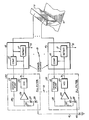
- a magnetic tape 10 is suitably transported past a multi-track transducer or head assembly 11.
- head 11 will have both recording and reading portions for each of the record tracks on tape 10.
- head 11 has 18 combinations of read gaps and write gaps.
- the invention relates to the frequency control of a reference clock used to generate timing or clock signals for reading data from magnetic tape 10. It is also to be understood that the details of the mechanism for transporting tape 10 and mounting head 11 are not shown for purposes of brevity.
- channel circuits 12, 13 and 14 There is one set of channel or readback circuits 12, 13 and 14 for each of the tracks on magnetic tape 10.
- the channel circuits provide data output over a set of lines 15 which are then phase synchronised for reconstructing the read data, as is known.
- Each of the channel circuits has its own frequency determining portion 20,21,22 (PLL filter) for generating the reference timing or clock signals.
- PLL filter frequency determining portion
- Channel circuits 13 and frequency determining portions (PLL filter) 21 are represented by dots to indicate channel circuits and PLL filters in addition to the circuits 12 and 14 and PLL filters 20 and 22 illustrated.
- the channel circuits 12 and 14, and the PLL filters 20 and 22 are brought out and expanded for illustrating the invention.
- phase comparator 16 compares the phase of the signal on line 31 supplied by the respective oscillator VCO 30 with the phase of the detector 17 input signal.
- Charge pump 18 supplies a charge pump signal over line 25.
- the charge pump signal is supplied through an RC circuit consisting of resistor 26, capacitor 27 and frequency determining capacitor 28 to a buffer amplifier 29 for controlling the frequency of operation of VCO 30.
- the frequency determining capacitor 28 is coupled to the ground reference potential as described below.
- the capacitance value of capacitor 28 is somewhat larger than the capacitance value of capacitor 27.
- a single capacitor 40 having a capacitance for determining with the capacitors 28 the frequencies of operation of the VCO's 30 is connected to all of the PLL filters 20, 21. and 22 of the system being described.
- the capacitors 28 have a substantially larger capacitance value than that of the capacitor 40, such as ten times the capacitance value.
- capacitor 40 is AC coupled to all of the PLL filters 20-22 but is DC isolated which enables the individual PLL filters 20-22 to compensate for any differences in VCO gains among the various phase-lock loops.
- the common capacitor 40 preferably has a capacitance value determined by a multiplicative factor of the number of tracks, i.e. the number VCO's 30 being commonly referenced to this single capacitor 40. For example, for a nine track grouping, the capacitor 40 is nine times the capacitance value of capacitor 28. In a group of eighteen PLL filters 20-22, the common capacitor 40 has eighteen times the capacitance value of the capacitor 28.
- the arrangement shown in the drawing gives a global clock effect for all of the channels by coupling together the frequency compensation portions of the PLL filters 20-22 from all the tracks through the coupling capacitors 28.
- the coupling capacitors 28 provide a DC or direct current blocking and respectively remain charged to the differences between the VCO gain for the respective tracks or channels; the average VCO gain of all of the tracks is coupled together through the common connection 41.
- Test operations of this circuit have shown that the individual channel circuits 12-14 are enabled to recover data better under marginal conditions by reducing the length of dropouts which then, of course, reduces dead tracking and enhances the recovery data integrity.
- An additional advantage of the illustrated arrangement is that the phase lock loop bandwidth for the individual channel circuits 12-14 can be decreased for improving signal to noise performance.
- the technique of providing a frequency reference to all of the phase lock loops can be used with other filter topologies or circuit arrangements from those illustrated in the drawing. The simplicity of the arrangement provides an enhanced operation without the attendant additional cost of a common clock or common VCO.
- Each of the channel circuits 15 includes a signal detection means 17 which receives the readback signal from head 11 and the clock signal over line 31 from the associated PLL filter.
- Detection means 17 includes the usual signal detection, error detection correction and other signal processing means found in such channel circuits.
- Phase comparator 16 compares the frequency in the phase of the clock signal on line 31 with the phase of the readback signal received from head 11.
- a phase error signal (from charge pump 18) is supplied over line 25 in the usual manner for slaving the operation of VCO 30 to the signal received from head 11.
- the VCO 30 may not faithfully follow the frequency and phase of the readback signal. Usually such degraded operation occurs in less than all of the channel circuits 12-14. The arrangement illustrated improves the accommodation of such signal quality variations.
Landscapes
- Engineering & Computer Science (AREA)
- Signal Processing (AREA)
- Signal Processing For Digital Recording And Reproducing (AREA)
- Stabilization Of Oscillater, Synchronisation, Frequency Synthesizers (AREA)
Applications Claiming Priority (2)
| Application Number | Priority Date | Filing Date | Title |
|---|---|---|---|
| US07/511,688 US5138282A (en) | 1990-04-20 | 1990-04-20 | Plural phase-lock loops sharing a common frequency control |
| US511688 | 1990-04-20 |
Publications (2)
| Publication Number | Publication Date |
|---|---|
| EP0453253A2 true EP0453253A2 (fr) | 1991-10-23 |
| EP0453253A3 EP0453253A3 (en) | 1993-01-13 |
Family
ID=24036013
Family Applications (1)
| Application Number | Title | Priority Date | Filing Date |
|---|---|---|---|
| EP19910303410 Ceased EP0453253A3 (en) | 1990-04-20 | 1991-04-17 | Timing signal generator for signal processing system |
Country Status (3)
| Country | Link |
|---|---|
| US (1) | US5138282A (fr) |
| EP (1) | EP0453253A3 (fr) |
| JP (1) | JPH0740407B2 (fr) |
Cited By (2)
| Publication number | Priority date | Publication date | Assignee | Title |
|---|---|---|---|---|
| EP0608014A3 (fr) * | 1993-01-20 | 1995-02-15 | Philips Electronics Nv | Dispositif de lecture de n/signaux numériques de n pistes adjacentes sur un support d'enregistrement. |
| EP0822664A2 (fr) | 1996-08-02 | 1998-02-04 | Texas Instruments Incorporated | Système et méthode de synchronisation de données |
Families Citing this family (5)
| Publication number | Priority date | Publication date | Assignee | Title |
|---|---|---|---|---|
| KR940011376B1 (ko) * | 1992-04-03 | 1994-12-07 | 삼성전자 주식회사 | Vtr의 캐리어 주파수 자동 조정 회로 |
| JP3267756B2 (ja) * | 1993-07-02 | 2002-03-25 | 株式会社日立製作所 | 半導体集積回路装置 |
| US6194929B1 (en) * | 1997-06-25 | 2001-02-27 | Sun Microsystems, Inc. | Delay locking using multiple control signals |
| US7860190B2 (en) * | 2007-03-19 | 2010-12-28 | Quantum Corporation | Multi-channel timing recovery system |
| US7885030B2 (en) * | 2008-07-07 | 2011-02-08 | International Business Machines Corporation | Methods and systems for delay compensation in global PLL-based timing recovery loops |
Family Cites Families (6)
| Publication number | Priority date | Publication date | Assignee | Title |
|---|---|---|---|---|
| GB1531632A (en) * | 1976-05-28 | 1978-11-08 | Westinghouse Brake & Signal | Phase-locked loop arrangements |
| US4433424A (en) * | 1981-05-11 | 1984-02-21 | International Business Machines Corporation | Multichannel common clock |
| US4470082A (en) * | 1982-07-06 | 1984-09-04 | Storage Technology Corporation | Digital clocking and detection system for a digital storage system |
| JPS62234476A (ja) * | 1986-04-04 | 1987-10-14 | Sony Corp | デイジタル映像信号再生装置 |
| AT386305B (de) * | 1986-07-08 | 1988-08-10 | Siemens Ag Oesterreich | Traegerfrequenz-station |
| US4825321A (en) * | 1987-05-20 | 1989-04-25 | Plus Development Corporation | Modular unitary disk file subsystem having increased data storage capacity |
-
1990
- 1990-04-20 US US07/511,688 patent/US5138282A/en not_active Expired - Fee Related
-
1991
- 1991-03-14 JP JP3103712A patent/JPH0740407B2/ja not_active Expired - Lifetime
- 1991-04-17 EP EP19910303410 patent/EP0453253A3/en not_active Ceased
Cited By (3)
| Publication number | Priority date | Publication date | Assignee | Title |
|---|---|---|---|---|
| EP0608014A3 (fr) * | 1993-01-20 | 1995-02-15 | Philips Electronics Nv | Dispositif de lecture de n/signaux numériques de n pistes adjacentes sur un support d'enregistrement. |
| EP0822664A2 (fr) | 1996-08-02 | 1998-02-04 | Texas Instruments Incorporated | Système et méthode de synchronisation de données |
| EP0822664A3 (fr) * | 1996-08-02 | 1999-08-18 | Texas Instruments Incorporated | Système et méthode de synchronisation de données |
Also Published As
| Publication number | Publication date |
|---|---|
| JPH04228152A (ja) | 1992-08-18 |
| JPH0740407B2 (ja) | 1995-05-01 |
| EP0453253A3 (en) | 1993-01-13 |
| US5138282A (en) | 1992-08-11 |
Similar Documents
| Publication | Publication Date | Title |
|---|---|---|
| US4069462A (en) | Phase-locked loops | |
| EP0663117B1 (fr) | Circuit de recuperation d'horloge pour echantillonnage de forme d'onde synchrone | |
| EP0189195B1 (fr) | Appareil pour la correction des erreurs de base de temps d'un signal vidéo | |
| CA1148653A (fr) | Oscillateur controle automatiquement par la phase | |
| EP0182701A2 (fr) | Boucle d'asservissement de phase pour l'enregistrement de données MFM | |
| US5206769A (en) | Method for controlling a plurality of phase-lock loops from a common frequency control | |
| US5272730A (en) | Digital phase-locked loop filter | |
| EP0122752A2 (fr) | Appareil d'enregistrement vidéo à bande numérique | |
| EP0453253A2 (fr) | Générateur de signaux d'horloge pour un système de traitement de signaux | |
| US3840892A (en) | Method and device for detecting signals from magnetic memory | |
| US5488516A (en) | Apparatus for reproducing n digital signals from n adjacent tracks on a record carrier | |
| JP2683483B2 (ja) | 表示画像の歪みを補正する信号処理装置 | |
| GB2084415A (en) | Apparatus for regenerating a clock pulse signal from a stream of data | |
| EP0597372B1 (fr) | Dispositifs de reproduction de signal digital, circuits intégrés à cet usage et méthodes de reproduction de signal digital | |
| US6097560A (en) | Reproducing apparatus having clock generator controlled by detected phase-difference and tendency of phase-difference | |
| CA1212178A (fr) | Circuit d'extraction de signaux | |
| US5260841A (en) | Clock extracting circuit | |
| US5245482A (en) | Magnetic recording/reproducing apparatus with skew correction | |
| JP3028819B2 (ja) | Pll回路のロツク,アンロツク検出回路 | |
| EP0623926A2 (fr) | Dispositif de lecture de n signaux numériques de n pistes adjacentes sur un support d'enregistrement | |
| US3747079A (en) | Reducing dead-tracking in recording systems | |
| JPH01155571A (ja) | クロック発生回路 | |
| EP1441519A1 (fr) | Dispositif de commande de vitesse de tambour à têtes pour appareil d'enregistrement à cassettes vidéo à définition standard. | |
| JPH08111070A (ja) | 再生装置 | |
| JPH03136413A (ja) | フェーズドロックループ回路 |
Legal Events
| Date | Code | Title | Description |
|---|---|---|---|
| PUAI | Public reference made under article 153(3) epc to a published international application that has entered the european phase |
Free format text: ORIGINAL CODE: 0009012 |
|
| AK | Designated contracting states |
Kind code of ref document: A2 Designated state(s): DE FR GB |
|
| 17P | Request for examination filed |
Effective date: 19911219 |
|
| PUAL | Search report despatched |
Free format text: ORIGINAL CODE: 0009013 |
|
| AK | Designated contracting states |
Kind code of ref document: A3 Designated state(s): DE FR GB |
|
| 17Q | First examination report despatched |
Effective date: 19950313 |
|
| STAA | Information on the status of an ep patent application or granted ep patent |
Free format text: STATUS: THE APPLICATION HAS BEEN REFUSED |
|
| 18R | Application refused |
Effective date: 19960624 |