EP0453324B1 - Aktiv-Matrix-Anzeigevorrichtung mit Dünnfilmtransistorstruktur - Google Patents
Aktiv-Matrix-Anzeigevorrichtung mit Dünnfilmtransistorstruktur Download PDFInfo
- Publication number
- EP0453324B1 EP0453324B1 EP91303580A EP91303580A EP0453324B1 EP 0453324 B1 EP0453324 B1 EP 0453324B1 EP 91303580 A EP91303580 A EP 91303580A EP 91303580 A EP91303580 A EP 91303580A EP 0453324 B1 EP0453324 B1 EP 0453324B1
- Authority
- EP
- European Patent Office
- Prior art keywords
- gate
- electrodes
- display device
- active matrix
- thin film
- Prior art date
- Legal status (The legal status is an assumption and is not a legal conclusion. Google has not performed a legal analysis and makes no representation as to the accuracy of the status listed.)
- Expired - Lifetime
Links
Images


Classifications
-
- G—PHYSICS
- G02—OPTICS
- G02F—OPTICAL DEVICES OR ARRANGEMENTS FOR THE CONTROL OF LIGHT BY MODIFICATION OF THE OPTICAL PROPERTIES OF THE MEDIA OF THE ELEMENTS INVOLVED THEREIN; NON-LINEAR OPTICS; FREQUENCY-CHANGING OF LIGHT; OPTICAL LOGIC ELEMENTS; OPTICAL ANALOGUE/DIGITAL CONVERTERS
- G02F1/00—Devices or arrangements for the control of the intensity, colour, phase, polarisation or direction of light arriving from an independent light source, e.g. switching, gating or modulating; Non-linear optics
- G02F1/01—Devices or arrangements for the control of the intensity, colour, phase, polarisation or direction of light arriving from an independent light source, e.g. switching, gating or modulating; Non-linear optics for the control of the intensity, phase, polarisation or colour
- G02F1/13—Devices or arrangements for the control of the intensity, colour, phase, polarisation or direction of light arriving from an independent light source, e.g. switching, gating or modulating; Non-linear optics for the control of the intensity, phase, polarisation or colour based on liquid crystals, e.g. single liquid crystal display cells
- G02F1/133—Constructional arrangements; Operation of liquid crystal cells; Circuit arrangements
- G02F1/136—Liquid crystal cells structurally associated with a semi-conducting layer or substrate, e.g. cells forming part of an integrated circuit
- G02F1/1362—Active matrix addressed cells
- G02F1/1368—Active matrix addressed cells in which the switching element is a three-electrode device
-
- H—ELECTRICITY
- H10—SEMICONDUCTOR DEVICES; ELECTRIC SOLID-STATE DEVICES NOT OTHERWISE PROVIDED FOR
- H10D—INORGANIC ELECTRIC SEMICONDUCTOR DEVICES
- H10D30/00—Field-effect transistors [FET]
- H10D30/60—Insulated-gate field-effect transistors [IGFET]
- H10D30/67—Thin-film transistors [TFT]
- H10D30/6729—Thin-film transistors [TFT] characterised by the electrodes
- H10D30/673—Thin-film transistors [TFT] characterised by the electrodes characterised by the shapes, relative sizes or dispositions of the gate electrodes
- H10D30/6732—Bottom-gate only TFTs
-
- H—ELECTRICITY
- H10—SEMICONDUCTOR DEVICES; ELECTRIC SOLID-STATE DEVICES NOT OTHERWISE PROVIDED FOR
- H10D—INORGANIC ELECTRIC SEMICONDUCTOR DEVICES
- H10D30/00—Field-effect transistors [FET]
- H10D30/60—Insulated-gate field-effect transistors [IGFET]
- H10D30/67—Thin-film transistors [TFT]
- H10D30/674—Thin-film transistors [TFT] characterised by the active materials
- H10D30/6741—Group IV materials, e.g. germanium or silicon carbide
- H10D30/6743—Silicon
- H10D30/6746—Amorphous silicon
-
- H—ELECTRICITY
- H10—SEMICONDUCTOR DEVICES; ELECTRIC SOLID-STATE DEVICES NOT OTHERWISE PROVIDED FOR
- H10D—INORGANIC ELECTRIC SEMICONDUCTOR DEVICES
- H10D30/00—Field-effect transistors [FET]
- H10D30/60—Insulated-gate field-effect transistors [IGFET]
- H10D30/67—Thin-film transistors [TFT]
- H10D30/6757—Thin-film transistors [TFT] characterised by the structure of the channel, e.g. transverse or longitudinal shape or doping profile
-
- H—ELECTRICITY
- H10—SEMICONDUCTOR DEVICES; ELECTRIC SOLID-STATE DEVICES NOT OTHERWISE PROVIDED FOR
- H10D—INORGANIC ELECTRIC SEMICONDUCTOR DEVICES
- H10D86/00—Integrated devices formed in or on insulating or conducting substrates, e.g. formed in silicon-on-insulator [SOI] substrates or on stainless steel or glass substrates
- H10D86/40—Integrated devices formed in or on insulating or conducting substrates, e.g. formed in silicon-on-insulator [SOI] substrates or on stainless steel or glass substrates characterised by multiple TFTs
Definitions
- the present invention relates generally to an active matrix display device, and more particularly to an active matrix display device using a display medium such as a liquid crystal and employing a switching device such as a thin film transistor (hereinafter called "TFT").
- TFT thin film transistor
- TFTs are in common use as a switching element for active matrix display devices.
- the TFTs used in the pixel electrodes reduce cross-talk between the pixels, and allow a limitless number of scanning lines.
- the active matrix display device has a larger capacity for display images and achieves a higher-precision image quality than a simple matrix display device.
- Gate buses 4 are arranged in parallel with each other on an active matrix substrate, with the interposition of pixel electrodes 5 between one gate bus and the adjacent gate bus.
- the gate buses in the odd-numbered order are indicated by 4a and those in the even-numbered order are indicated by 4b .
- the pixel electrodes connected to the gate buses 4a are indicated by 5a
- those connected to the gate buses 4b are indicated by 5b .
- the pixel electrodes 5a and 5b arranged in columns in parallel with the gate bases 5a and 5b are aligned with each other, and those in the adjacent columns are displaced from each other by half the side of each pixel electrode along the gate buses 4a and 4b .
- Three pixel electrodes arranged in a triangle displaying red, green and blue constitute a unit.
- Source buses 6 are arranged in a zig-zag form among the pixel electrodes 5a and 5b .
- the pixel electrode 5a is provided with a TFT 1 ( Figure 8) which comprises a TFT 1a connected to the gate bus 4a or a TFT 1b connected to the gate bus 4b .
- the TFT 1a is formed on a gate electrode 10a extended from the gate bus 4a at a right angle thereto.
- the pixel electrodes 5a are connected to drain electrodes 8a of the TFT 1a , and a source electrode 9a of the TFT 1a is connected to the source bus 6 .
- the TFT 1b is formed on a gate electrode 10b extended from the gate bus 4b at a right angle.
- the pixel electrode 5b is connected to a drain electrode 8b .
- the source electrode 9b of the TFT 1b is connected to the source bus 6 .
- the position of the drain electrode 8a to the gate electrode 10a of the TFT 1a and that of the drain electrode 8b to the gate electrode 10b of the TFT 1b are mutually in opposite directions along the extension of the gate bus 4 .
- Additional capacitor lines 7 are provided for each pixel electrode 5 . Part of each additional capacitor line 7 functions as an additional capacitor electrode for the pixel electrode 5 . In Figure 4, the additional capacitor line 7 is omitted.
- the TFT 1a has the gate electrode 10a patterned on the glass substrate 21 and an anode oxidized film layer 22 wholly covered with a gate insulating layer 23 .
- a gate insulating layer 23 On the gate insulating layer 23 are a channel layer 24 , a channel protective layer 25 , a contact layer 26 , a source metal layer 19a and a drain metal layer 18a .
- the pixel electrodes 5a are formed with ITO (Indium Tin Oxide) on the drain metal layer 18a .
- An ITO layer 27 is formed at the same time as the pixel electrodes 5a are formed.
- the contact layer 26 and the drain metal layer 18a constitute the source electrode 9a .
- the contact layer 26 and the drain metal layer 18a constitute the drain electrode 8a .
- FIG 8 is an equivalent circuit for the active matrix substrate described above.
- the TFTs 1 of this active matrix substrate are connected to a pixel capacitor 11 constituted by the pixel electrode 5 and a counter electrode, and a liquid crystal layer, an additional capacitor 12 constituted by a pixel electrode 5 , the gate insulating layer 23 and the additional capacitor line 7 , and a parasitic capacitance 13 constituted by the gate electrode 10a (or 10b ).
- the parasitic capacitance 13 is formed in the overlapping portions of the gate electrode 10a (or 10b ) and the drain electrode 8a (or 8b ).
- the overlapping portions are indicated by hatching, having an area of X x W. If the drain electrode 8a is formed at a displaced position, the parasitic capacitance will have a different capacity.
- the position of the drain electrode 8a to the gate electrode 10a of the TFT 1a and that of the drain electrode 8b to the gate electrode 10b of the TFT 1b are mutually in opposite directions along the extension of the gate bus 4 .
- the drain electrodes 8a and 8b of the TFTs 1a and 1b are formed by patterning. If they are formed at displaced positions from predetermined positions along the extension of the gate bus 4 , the area of the overlapping portions of the gate electrode 10a and the drain electrode 8a of the TFT 1a will be different from that of the overlapping portions of the gate electrode 10b and the drain electrode 8b of the TFT 1b . As a result, the parasitic capacitance connected to the TFT 1a and that connected to the TFT 1b will become different in value.
- an a.c. signal applied to the drain electrode 8 from the source electrode 9 is transiently distributed to the pixel capacitor 11 , the parasitic capacitor 13 , and the additional capacitor 12 .
- the parasitic capacitor of the TFT is greater than that of a MOS-FET, and owing to it, the voltage waveform of the a.c. signal becomes unsymmetrical. The non-symmetry causes an off-set DC voltage component, and thereby causes detrimental flicker.
- the common practice is to apply a DC component to the counter electrodes located on the opposite side of the liquid crystal layer, so as to compensate for the off-set DC voltage.
- the voltage applied to the counter electrodes can only compensate for the parasitic capacitance either of the TFT 1a or the TFT 1b.
- a DC component is applied to the pixel electrodes 5 connected to the TFT 1 whose parasitic capacitance is not compensated.
- the display device is subject to flicker.
- the document EP-A-0 112 700 discloses a structure according to the preamble of claim 1 wherein a picture electrode connected between two address lines is connected to one of the address lines through a TFT, and a storage capacitor is formed between the pixel electrode and the other address line.
- EP-A-0 185 995 discloses a display having two n-i-n diodes connected in series between a pixel electrode and an address line.
- an active matrix display device in which a matrix array of pixel electrodes is formed on the inside surface of one of a pair of superposed insulating substrates, the voltage applied to each said pixel electrode being controlled by a respective thin film transistor device including a gate electrode connector connected to a gate bus and a drain electrode connector connected to the pixel electrode, characterised in that the thin film transistor device includes a pair of thin film transistors spaced apart along the gate bus, and arranged with their gate electrodes extending laterally from said gate bus and disposed symmetrically about an intermediate central plane, the drain electrodes of said pair of thin film transistors being arranged substantially symmetrically about said central plane.
- the pixel electrodes are arranged in lines parallel to the gate buses, and the pixel electrodes in adjacent lines are displaced from each other by half the width of each pixel electrode as measured along the gate buses.
- the pixel electrodes are connected to source buses arranged in a zigzag form therebetween.
- the present invention described herein makes possible of the objective of providing an active matrix display device which ensures that no flicker occurs even if TFTs have different parasitic capacitances.
- a pixel electrode is provided with one or more pairs of TFTs, each pair of TFTs having gate electrodes and drain electrodes each formed in symmetrical shapes with respect to a central plane passing through a center between the paired TFTs.
- the gate electrodes of each pair of TFTs are positioned perpendicular to the gate buses. This arrangement is advantageous in that if the drain electrode is patterned at a displaced position in the direction of the gate buses, one of the TFTs has an increased overlapping portion of the gate electrode and the drain electrode wherein the other TFT has a decreased overlapping portion thereof.
- the parasitic capacitances of the TFTs are kept constant irrespective of the displacement of the drain electrodes, thereby keeping the display device free from flicker due to differentiated parasitic capacitances.
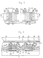
- a plurality of pixel electrodes 55 are formed on an insulated substrate, with gate buses 54 interposed in parallel between one pixel electrode 55 and the next.
- the gate bus 54 comprises a gate bus 54a or 54b
- the pixel electrode 55 comprises a pixel electrode 55a connected to the gate bus 54a or a pixel electrode 55b connected to the gate bus 54b .
- the pixel electrodes 55a and 55b in each columns in parallel with the gate buses 54a and 54b are aligned with each other, and those in adjacent columns are displaced from each other by half the side of the pixel electrode along the gate buses 54a and 54b as shown in Figure 1.
- the source buses 56 are formed in a zigzag form among the pixel electrodes 55a and 55b .
- the TFTs 51a and 61a are provided between the gate bus 54a and the pixel electrode 55a .
- the TFTs 51b and 61b are provided between the gate bus 54b and the pixel electrode 55b .
- the TFTs 51b and 61b are formed on the gate electrodes 57a and 67a extended from the gate bus 54a at a right angle thereto.
- the gate electrodes 57a and 67a , the drain electrodes 58a and 68a , and the source electrodes 59a and 69a of the TFTs 51a and 61a are symmetrically formed with respect to a central plane located at the center between the TFTs 51a and 61a .
- the pixel electrode 55a is connected to the drain electrodes 58a and 68a of the TFTs 51a and 61a .
- the source electrodes 59a and 69a of the TFTs 51a and 61a are connected to an extension 90a of the source bus 56 .
- the TFTs 51b and 61b are formed on the gate electrodes 57b and 67b extended from the gate bus 54b at a right angle thereto.
- the gate electrodes 57b and 67b , the drain electrodes 58b and 68b , and the source electrodes 59b and 69b of the TFTs 51b and 61b are symmetrically formed with respect to a central plane located at the center between the TFTs 51b and 61b .
- the pixel electrode 55b is connected to the drain electrodes 58b and 68b of the TFTs 51b and 61b .
- the source electrodes 59b and 69b of the TFTs 51b and 61b are connected to an extension 90b of the source bus 56 .
- An additional capacitor line 91 is provided for each of the pixel electrodes 55a , 55b . Part of the additional capacitor lines 91 functions as additional capacitor electrodes against the respective pixel electrodes 55 .
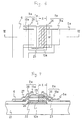
- a glass substrate 71 was prepared, on which a film having a thickness of 3000 ⁇ was formed with Ta.
- the Ta film was patterned by photolithography or etching so as to form the gate buses 54a and 54b , the gate electrodes 57a , 57b , 67a and 67b , and the additional capacitor lines 91 were formed.
- the gate buses 54a and 54b , the gate electrodes 57a , 57b , 67a and 67b , and the additional capacitor lines 91 were subjected to surface anodizing. In this way these lines and electrodes were covered with anodized layer 72 of Ta2O5.
- a gate insulating layer 73 having a thickness of 3000 ⁇ was formed with silicon nitride (SiN x ) by a plasma CVD method so as to cover the whole surface of the anodized layer 27 .
- the gate insulating layer 73 was covered with an intrinsic amorphous silicon (a-Si(i)) layer having a thickness of 300 ⁇ , which formed channel layers 74 at a later stage, and a silicon nitride layer having a thickness of 2000 ⁇ which formed channel protective layers 75 .
- the silicon nitride layer was patterned by photolithography but of course it can be done by etching so as to form the channel protective layers 75 on the gate electrodes 57a , 57b , 67a and 67b .
- an n-type amorphous silicon (a-Si(n+)) layer was deposited by a CVD method, so as to form contact layers 76 and 86 at a later stage.
- the a-Si(i) layer and the a-Si(n+) layer were patterned by photolithography and etching. In this way the contact layers 76 and 86 , and the channel layers 74 were formed. At this stage, the contact layers 76 and 86 are connected to each other on the channel layers 74 .
- a metal layer was formed with Ti having a thickness of 3000 ⁇ by sputtering.
- the Ti layer was patterned by photolithography and etching so as to form the source bus 56 , the extensions 90a and 90b , the source metal layers 89a , 89b , 99a and 99b , the source metal layers 89a , 89b , 99a and 99b , and the drain metal layers 88a , 88b , 98a and 98b .
- the channel protective layer 75 for the contact layers 76 and 86 and a central portion of the channel protective layer 75 were removed by etching.
- the contact layer 76 and the source metal layer 89a constituted the source electrode 59a
- the contact layer 86 and the source metal layer 99a constituted the source metal layer 69a
- the contact layer 86 and the drain metal layer 98a constituted the drain electrode 68a .
- an ITO layer having a thickness of 1000 ⁇ was formed by sputtering.
- the ITO layer was patterned by photolithography and etching so as to form pixel electrodes 55a and 55b .
- the ITO layer 77 was retained on the source bus 56, the extensions 90a and 90b , the source metal layers 89a , 89b , 99a , and 99b , the drain metal layers 88a , 88b , 98a and 98b .
- a protective layer 92 having a thickness of 3000 ⁇ was formed with SiN x , on which an orientation layer 93 was additionally formed.
- the counter substrate 81 On the counter substrate 81 were formed a black stripe 82 and a color filter 83 , and the counter electrode 84 of ITO and an orientation layer 85 were formed over the black stripe 82 and the color filter 83 .
- the liquid crystal layer 94 is sandwiched between the two substrates 71 and 81 . In this way the active matrix display device is finished.
- the parasitic capacitance is formed in the portion indicated by hatching in Figure 2: more specifically, the overlapping region A of the gate electrode 57a and the drain electrode 58a , and the overlapping region B of the gate electrode 67a and the drain electrode 68a .
- the areas SA of the region A and the area SB of the region B are equal in having the size of ( X x W ), where the X is the length of a minor side of the regions A and B along the gate bus 54 , and the W is the length of a major side of the regions A and B in the direction perpendicular to the gate bus 54 .
- the gate electrodes 57a and 67a are symmetrically disposed on opposite sides of an imaginary central plane situated at a center between the TFTs 51a and 61a .
- Each gate electrode 57a and 57b is perpendicular to the gate buses 54 .
- the drain electrodes 58a and 68a of the TFTs 51a and 61a are formed in symmetrical forms with respect to the imaginary central plane. This arrangement ensures that even if the drain electrodes 58a and 68a are displaced from a predetermined position in the direction of the gate bus 54 , the total area of the regions A and B remains constant.
- the total of SA and SB is 2X x W. This means that the total area remains the same as if no displacement occurs in the positions of the drain electrodes 58a and 68a . This effect is also present in the TFTs 51b and 61b .
- a pair of TFTs are provided for a single pixel electrode, but the number of TFTs is not limited to one pair. A greater number of TFTs can be employed. When two or more pairs of TFTs are employed, it is only necessary to ensure that the gate electrodes and the drain electrodes of the TFTs of each pair are symmetrical with respect to the imaginary central plane passing through a center between the respective pair of TFTs.
- each pixel electrode is provided with at least a pair of TFTs including gate electrodes and drain electrodes, wherein the gate electrodes are formed in symmetrical shapes with respect to a central plane passing through a center between the pair of TFTs.
- the known high-precision, small-size active matrix display device reduces the display performance because of the low numerical aperture.
- a display device having a large area covered by the light shield layer is used for a projection type display device, another problem arises as black spots in the image picture resulting from the light shield layers.
Landscapes
- Physics & Mathematics (AREA)
- Nonlinear Science (AREA)
- Engineering & Computer Science (AREA)
- Microelectronics & Electronic Packaging (AREA)
- Mathematical Physics (AREA)
- Chemical & Material Sciences (AREA)
- Crystallography & Structural Chemistry (AREA)
- General Physics & Mathematics (AREA)
- Optics & Photonics (AREA)
- Liquid Crystal (AREA)
- Devices For Indicating Variable Information By Combining Individual Elements (AREA)
- Thin Film Transistor (AREA)
Claims (7)
- Aktivmatrix-Anzeigevorrichtung, bei der eine Matrixanordnung aus Pixelelektroden (55a, 55b) auf der Innenfläche eines Paars übereinanderliegender isolierender Substrate ausgebildet ist, wobei die an jede Pixelelektrode angelegte Spannung durch ein jeweiliges Dünnfilmtransistor-Bauteil mit einem mit einem Gatebus (54a; 54b) verbundenen Gateelektrode-Abschnitt und einem mit der Pixelelektrode verbundenen Drainelektrode-Abschnitt gesteuert wird, dadurch gekenn zeichnet, daß das Dünnfilmtransistor-Bauteil ein Paar entlang des Gatebusses voneinander beabstandeter Dünnfilmtransistoren (51a, 61a; 51b, 61b) aufweist, die so angeordnet sind, daß sich ihre Gateelektroden (57a, 67a; 57b, 67b) in Querrichtung ausgehend vom Gatebus erstrecken und symmetrisch in bezug auf eine Mittelebene angeordnet sind, wobei die Drainelektroden (58a, 68a; 58b, 68b) des Paars Dünnfilmtransistoren im wesentlichen symmetrisch zur Mittelebene angeordnet sind.
- Aktivmatrix-Anzeigevorrichtung nach Anspruch 1, bei der die Pixelelektroden (55a, 55b)in Linien parallel zu den Gatebussen (54a, 54b) angeordnet sind und die Pixelelektroden in benachbarten Linien gegeneinander um die Hälfte der Breite jeder Pixelelektrode gemessen entlang der Gatebusse versetzt sind.
- Aktivmatrix-Anzeigevorrichtung nach Anspruch 1 oder Anspruch 2, bei der die Pixelelektroden (55a, 55b) über die Paare von Dünnfilmtransistoren (51a, 61a; 51b, 61b) mit zickzackförmig dazwischenliegenden Sourcebussen (56) verbunden sind.
- Aktivmatrix-Anzeigevorrichtung nach Anspruch 1, ferner mit Sourcebussen (56), die zwischen den Pixelelektroden (55a, 55b) angeordnet sind und die Gatebusse (54a, 54b) rechtwinklig schneiden, wobei jeder Sourcebus über einen verlängerten Abschnitt (90a, 90b) mit einem Endabschnitt verfügt, der mit den Sourceelektroden der Dünnfilmtransistoren verbunden ist, sich rechtwinklig zu den Gatebussen erstreckt und mit der Mittelebene jedes Paars Dünnfilmtransistoren (51a, 61a; 51b, 61b) zusammenfällt.
- Aktivmatrix-Anzeigevorrichtung nach Anspruch 4, bei der die Pixelelektroden (55a, 55b) über die Paare von Dünnfilmtransistoren (51a, 61a; 51b, 61b) mit den zickzackförmig dazwischen angeordneten Sourcebussen (56) verbunden sind.
- Aktivmatrix-Anzeigevorrichtung nach Anspruch 5, bei der die mit irgendeinem vorgegebenen Sourcebus (56) verbundenen Pixelelektroden (55a, 55b) auf abwechselnden Seiten entlang des Sourcebusses angeordnet sind.
- Aktivmatrix-Anzeigevorrichtung nach einem der Ansprüche 4 bis 6, bei der die Pixelelektroden (55a, 55b) in Linien parallel zu den Gatebussen (54a, 54b) angeordnet sind und die Pixelelektroden in benachbarten Linien gegeneinander um die Hälfte der Breite jeder Pixelelektrode gemessen entlang den Gatebussen versetzt sind.
Applications Claiming Priority (2)
| Application Number | Priority Date | Filing Date | Title |
|---|---|---|---|
| JP10598290A JPH0830825B2 (ja) | 1990-04-20 | 1990-04-20 | アクティブマトリクス表示装置 |
| JP105982/90 | 1990-10-11 |
Publications (3)
| Publication Number | Publication Date |
|---|---|
| EP0453324A2 EP0453324A2 (de) | 1991-10-23 |
| EP0453324A3 EP0453324A3 (en) | 1992-04-15 |
| EP0453324B1 true EP0453324B1 (de) | 1995-06-21 |
Family
ID=14421955
Family Applications (1)
| Application Number | Title | Priority Date | Filing Date |
|---|---|---|---|
| EP91303580A Expired - Lifetime EP0453324B1 (de) | 1990-04-20 | 1991-04-22 | Aktiv-Matrix-Anzeigevorrichtung mit Dünnfilmtransistorstruktur |
Country Status (5)
| Country | Link |
|---|---|
| US (1) | US5191451A (de) |
| EP (1) | EP0453324B1 (de) |
| JP (1) | JPH0830825B2 (de) |
| KR (1) | KR940006989B1 (de) |
| DE (1) | DE69110531T2 (de) |
Families Citing this family (32)
| Publication number | Priority date | Publication date | Assignee | Title |
|---|---|---|---|---|
| JP3255942B2 (ja) * | 1991-06-19 | 2002-02-12 | 株式会社半導体エネルギー研究所 | 逆スタガ薄膜トランジスタの作製方法 |
| US5285302A (en) * | 1992-03-30 | 1994-02-08 | Industrial Technology Research Institute | TFT matrix liquid crystal display with compensation capacitance plus TFT stray capacitance constant irrespective of mask misalignment during patterning |
| JP2823178B2 (ja) * | 1992-04-06 | 1998-11-11 | シャープ株式会社 | 金属配線基板及びその製造方法 |
| JP2814161B2 (ja) * | 1992-04-28 | 1998-10-22 | 株式会社半導体エネルギー研究所 | アクティブマトリクス表示装置およびその駆動方法 |
| US6693681B1 (en) | 1992-04-28 | 2004-02-17 | Semiconductor Energy Laboratory Co., Ltd. | Electro-optical device and method of driving the same |
| JP2635885B2 (ja) * | 1992-06-09 | 1997-07-30 | インターナショナル・ビジネス・マシーンズ・コーポレイション | 薄膜トランジスタ及びアクティブマトリクス液晶表示装置 |
| EP0582387B1 (de) * | 1992-08-05 | 1999-05-26 | Sharp Kabushiki Kaisha | Metallische Leiterplatte und Herstellungsverfahren dafür |
| US6094252A (en) * | 1995-09-05 | 2000-07-25 | Sharp Kabushiki Kaisha | GH LCD having particular parameters and characteristics |
| KR100430798B1 (ko) * | 1995-12-29 | 2004-07-19 | 삼성전자주식회사 | 액정표시장치용박막트랜지스터기판 |
| KR100209620B1 (ko) * | 1996-08-31 | 1999-07-15 | 구자홍 | 액정 표시 장치 및 그 제조방법 |
| JP3036513B2 (ja) | 1998-06-10 | 2000-04-24 | 日本電気株式会社 | 液晶表示装置 |
| WO2001048546A1 (en) * | 1999-12-24 | 2001-07-05 | Matsushita Electric Industrial Co., Ltd. | Liquid crystal device |
| KR100494702B1 (ko) * | 2001-12-26 | 2005-06-13 | 비오이 하이디스 테크놀로지 주식회사 | 프린지 필드 스위칭 액정표시장치 |
| JP3872377B2 (ja) * | 2002-04-30 | 2007-01-24 | インターナショナル・ビジネス・マシーンズ・コーポレーション | 画像表示素子および画像表示装置 |
| KR100918180B1 (ko) * | 2003-03-04 | 2009-09-22 | 삼성전자주식회사 | 쉬프트 레지스터 |
| US7209105B2 (en) * | 2003-06-06 | 2007-04-24 | Clairvoyante, Inc | System and method for compensating for visual effects upon panels having fixed pattern noise with reduced quantization error |
| US7218301B2 (en) * | 2003-06-06 | 2007-05-15 | Clairvoyante, Inc | System and method of performing dot inversion with standard drivers and backplane on novel display panel layouts |
| US20040246280A1 (en) * | 2003-06-06 | 2004-12-09 | Credelle Thomas Lloyd | Image degradation correction in novel liquid crystal displays |
| US8035599B2 (en) | 2003-06-06 | 2011-10-11 | Samsung Electronics Co., Ltd. | Display panel having crossover connections effecting dot inversion |
| US7397455B2 (en) * | 2003-06-06 | 2008-07-08 | Samsung Electronics Co., Ltd. | Liquid crystal display backplane layouts and addressing for non-standard subpixel arrangements |
| US7187353B2 (en) * | 2003-06-06 | 2007-03-06 | Clairvoyante, Inc | Dot inversion on novel display panel layouts with extra drivers |
| US7791679B2 (en) * | 2003-06-06 | 2010-09-07 | Samsung Electronics Co., Ltd. | Alternative thin film transistors for liquid crystal displays |
| TWI226962B (en) | 2004-01-05 | 2005-01-21 | Au Optronics Corp | Liquid crystal display device with a capacitance-compensated structure |
| US7268758B2 (en) | 2004-03-23 | 2007-09-11 | Clairvoyante, Inc | Transistor backplanes for liquid crystal displays comprising different sized subpixels |
| KR20060046241A (ko) * | 2004-06-29 | 2006-05-17 | 엘지.필립스 엘시디 주식회사 | 액정표시소자 |
| JP2008223775A (ja) * | 2007-03-08 | 2008-09-25 | Jtekt Corp | 車輪支持装置 |
| US8259228B2 (en) * | 2007-12-10 | 2012-09-04 | Ati Technologies Ulc | Method and apparatus for high quality video motion adaptive edge-directional deinterlacing |
| CN102520555A (zh) * | 2011-12-02 | 2012-06-27 | 深圳市华星光电技术有限公司 | 一种像素结构、阵列基板和液晶显示装置 |
| TWI559046B (zh) * | 2012-03-30 | 2016-11-21 | 友達光電股份有限公司 | 畫素陣列及顯示面板 |
| CN102881249A (zh) * | 2012-10-18 | 2013-01-16 | 深圳市华星光电技术有限公司 | 像素单元及主动矩阵式平面显示装置 |
| TWI522716B (zh) | 2013-05-10 | 2016-02-21 | 群創光電股份有限公司 | 薄膜電晶體基板及顯示裝置 |
| CN104142594B (zh) * | 2013-05-10 | 2017-06-06 | 群创光电股份有限公司 | 薄膜晶体管基板及显示装置 |
Family Cites Families (16)
| Publication number | Priority date | Publication date | Assignee | Title |
|---|---|---|---|---|
| JPS59119390A (ja) * | 1982-12-25 | 1984-07-10 | 株式会社東芝 | 薄膜トランジスタ回路 |
| US4698627A (en) * | 1984-04-25 | 1987-10-06 | Energy Conversion Devices, Inc. | Programmable semiconductor switch for a light influencing display and method for making same |
| US4775861A (en) * | 1984-11-02 | 1988-10-04 | Nec Corporation | Driving circuit of a liquid crystal display panel which equivalently reduces picture defects |
| DE3581498D1 (de) * | 1984-11-16 | 1991-02-28 | Matsushita Electric Industrial Co Ltd | Aktive matrixschaltung fuer fluessigkristallanzeigen. |
| EP0189214B1 (de) * | 1985-01-25 | 1997-07-23 | Nec Corporation | Aufbau eines Flüssigkristall-Mehrfarbenanzeigepaneels |
| FR2581783B1 (fr) * | 1985-05-07 | 1989-05-12 | Commissariat Energie Atomique | Dispositif d'affichage a matrice active et a commande integree comprenant deux familles d'electrodes lignes et deux familles d'electrodes colonnes par point image et son procede de commande |
| FR2593632B1 (fr) * | 1986-01-27 | 1988-03-18 | Maurice Francois | Ecran d'affichage a matrice active et procedes de realisation de cet ecran |
| GB8604402D0 (en) * | 1986-02-21 | 1986-03-26 | Gen Electric Co Plc | Liquid crystal displays |
| US4762398A (en) * | 1987-01-26 | 1988-08-09 | Hosiden Electronics Co., Ltd. | Pixel transistor free of parasitic capacitance fluctuations from misalignment |
| JPS63186216A (ja) * | 1987-01-28 | 1988-08-01 | Nec Corp | アクテイブマトリツクス液晶表示器 |
| JPS63262621A (ja) * | 1987-04-21 | 1988-10-28 | Alps Electric Co Ltd | 薄膜トランジスタアレイのトリミング方法 |
| JPS63263743A (ja) * | 1987-04-22 | 1988-10-31 | Alps Electric Co Ltd | 薄膜トランジスタアレイおよびその製法 |
| JPH0193121A (ja) * | 1987-10-05 | 1989-04-12 | Kawasaki Steel Corp | 半導体ウェハベーキング装置 |
| JPH021823A (ja) * | 1988-06-10 | 1990-01-08 | Fujitsu Ltd | アクティブマトリクス型液晶表示装置 |
| US4917467A (en) * | 1988-06-16 | 1990-04-17 | Industrial Technology Research Institute | Active matrix addressing arrangement for liquid crystal display |
| JPH0235493A (ja) * | 1988-07-26 | 1990-02-06 | Sony Corp | ディスプレイ装置 |
-
1990
- 1990-04-20 JP JP10598290A patent/JPH0830825B2/ja not_active Expired - Lifetime
-
1991
- 1991-04-16 US US07/685,680 patent/US5191451A/en not_active Expired - Lifetime
- 1991-04-19 KR KR1019910006312A patent/KR940006989B1/ko not_active Expired - Lifetime
- 1991-04-22 DE DE69110531T patent/DE69110531T2/de not_active Expired - Fee Related
- 1991-04-22 EP EP91303580A patent/EP0453324B1/de not_active Expired - Lifetime
Also Published As
| Publication number | Publication date |
|---|---|
| DE69110531D1 (de) | 1995-07-27 |
| EP0453324A2 (de) | 1991-10-23 |
| JPH0830825B2 (ja) | 1996-03-27 |
| EP0453324A3 (en) | 1992-04-15 |
| KR940006989B1 (ko) | 1994-08-03 |
| US5191451A (en) | 1993-03-02 |
| JPH043124A (ja) | 1992-01-08 |
| KR910018836A (ko) | 1991-11-30 |
| DE69110531T2 (de) | 1996-01-18 |
Similar Documents
| Publication | Publication Date | Title |
|---|---|---|
| EP0453324B1 (de) | Aktiv-Matrix-Anzeigevorrichtung mit Dünnfilmtransistorstruktur | |
| EP0668528B1 (de) | Dünnfilm-Feldeffekt-Transistormatrix zur Verwendung in Flüssigkristallanzeigen mit aktiver Matrix | |
| KR100997965B1 (ko) | 액정 표시 장치 | |
| KR100209471B1 (ko) | 박막트랜지스터 | |
| US6310668B1 (en) | LCD wherein opening in source electrode overlaps gate electrode to compensate variations in parasitic capacitance | |
| US8217872B2 (en) | Active matrix substrate, and liquid crystal display device | |
| US6226057B1 (en) | Liquid crystal display having overlapped pixel electrodes and method for fabricating the same | |
| US7973899B2 (en) | Thin film transistor array panel with capacitive coupling between adjacent pixel areas | |
| JP3582193B2 (ja) | 液晶表示素子 | |
| KR100360753B1 (ko) | 액정표시장치 및 그 제조방법 | |
| US20130153906A1 (en) | Thin film transistor array panel having improved storage capacitance and manufacturing method thereof | |
| KR101209050B1 (ko) | 액정 표시 장치 및 그 검사 방법 | |
| KR100474529B1 (ko) | 반사형액정표시장치및그제조방법 | |
| KR101420731B1 (ko) | 박막 트랜지스터 기판 및 이를 구비하는 액정 표시 장치 | |
| KR19980041737A (ko) | 액정디스플레이장치 및 그 제조방법 | |
| JP3127619B2 (ja) | アクティブマトリクス基板 | |
| JP2002530719A (ja) | 能動マトリックス液晶ディスプレイデバイス | |
| KR101230301B1 (ko) | 액정 표시 장치 및 그 구동 방법 | |
| US20060157705A1 (en) | Thin film transistor array panel | |
| KR100205378B1 (ko) | 액티브 매트릭스 액정표시소자 | |
| JPH0611735A (ja) | 光学的マスクを有するディスプレイスクリーンおよびスクリーンの形成法 | |
| KR20000040730A (ko) | 액정표시장치의 축적캐패시터 구조 및 그 제조방법 | |
| JPH07325322A (ja) | 薄膜トランジスタ液晶表示装置 | |
| JPH0797190B2 (ja) | 記憶装置および液晶表示装置 | |
| JP2541446B2 (ja) | アクティブマトリックスパネル |
Legal Events
| Date | Code | Title | Description |
|---|---|---|---|
| PUAI | Public reference made under article 153(3) epc to a published international application that has entered the european phase |
Free format text: ORIGINAL CODE: 0009012 |
|
| 17P | Request for examination filed |
Effective date: 19910516 |
|
| AK | Designated contracting states |
Kind code of ref document: A2 Designated state(s): DE FR GB NL |
|
| PUAL | Search report despatched |
Free format text: ORIGINAL CODE: 0009013 |
|
| AK | Designated contracting states |
Kind code of ref document: A3 Designated state(s): DE FR GB NL |
|
| 17Q | First examination report despatched |
Effective date: 19940225 |
|
| RAP1 | Party data changed (applicant data changed or rights of an application transferred) |
Owner name: SHARP KABUSHIKI KAISHA |
|
| GRAA | (expected) grant |
Free format text: ORIGINAL CODE: 0009210 |
|
| AK | Designated contracting states |
Kind code of ref document: B1 Designated state(s): DE FR GB NL |
|
| REF | Corresponds to: |
Ref document number: 69110531 Country of ref document: DE Date of ref document: 19950727 |
|
| ET | Fr: translation filed | ||
| PLBE | No opposition filed within time limit |
Free format text: ORIGINAL CODE: 0009261 |
|
| STAA | Information on the status of an ep patent application or granted ep patent |
Free format text: STATUS: NO OPPOSITION FILED WITHIN TIME LIMIT |
|
| 26N | No opposition filed | ||
| PGFP | Annual fee paid to national office [announced via postgrant information from national office to epo] |
Ref country code: FR Payment date: 20010409 Year of fee payment: 11 |
|
| PGFP | Annual fee paid to national office [announced via postgrant information from national office to epo] |
Ref country code: GB Payment date: 20010418 Year of fee payment: 11 Ref country code: DE Payment date: 20010418 Year of fee payment: 11 |
|
| PGFP | Annual fee paid to national office [announced via postgrant information from national office to epo] |
Ref country code: NL Payment date: 20010430 Year of fee payment: 11 |
|
| REG | Reference to a national code |
Ref country code: GB Ref legal event code: IF02 |
|
| PG25 | Lapsed in a contracting state [announced via postgrant information from national office to epo] |
Ref country code: GB Free format text: LAPSE BECAUSE OF NON-PAYMENT OF DUE FEES Effective date: 20020422 |
|
| PG25 | Lapsed in a contracting state [announced via postgrant information from national office to epo] |
Ref country code: NL Free format text: LAPSE BECAUSE OF NON-PAYMENT OF DUE FEES Effective date: 20021101 Ref country code: DE Free format text: LAPSE BECAUSE OF NON-PAYMENT OF DUE FEES Effective date: 20021101 |
|
| GBPC | Gb: european patent ceased through non-payment of renewal fee |
Effective date: 20020422 |
|
| PG25 | Lapsed in a contracting state [announced via postgrant information from national office to epo] |
Ref country code: FR Free format text: LAPSE BECAUSE OF NON-PAYMENT OF DUE FEES Effective date: 20021231 |
|
| NLV4 | Nl: lapsed or anulled due to non-payment of the annual fee |
Effective date: 20021101 |
|
| REG | Reference to a national code |
Ref country code: FR Ref legal event code: ST |