EP0454499B1 - Méthode pour évaluer une couche mince de lithium niobate et appareil pour le préparer - Google Patents
Méthode pour évaluer une couche mince de lithium niobate et appareil pour le préparer Download PDFInfo
- Publication number
- EP0454499B1 EP0454499B1 EP91303850A EP91303850A EP0454499B1 EP 0454499 B1 EP0454499 B1 EP 0454499B1 EP 91303850 A EP91303850 A EP 91303850A EP 91303850 A EP91303850 A EP 91303850A EP 0454499 B1 EP0454499 B1 EP 0454499B1
- Authority
- EP
- European Patent Office
- Prior art keywords
- thin film
- composition ratio
- absorption edge
- film
- edge wavelength
- Prior art date
- Legal status (The legal status is an assumption and is not a legal conclusion. Google has not performed a legal analysis and makes no representation as to the accuracy of the status listed.)
- Expired - Lifetime
Links
- 239000010409 thin film Substances 0.000 title claims description 76
- 238000000034 method Methods 0.000 title claims description 26
- GQYHUHYESMUTHG-UHFFFAOYSA-N lithium niobate Chemical compound [Li+].[O-][Nb](=O)=O GQYHUHYESMUTHG-UHFFFAOYSA-N 0.000 title claims description 19
- 239000000203 mixture Substances 0.000 claims description 63
- 238000010521 absorption reaction Methods 0.000 claims description 52
- 239000010955 niobium Substances 0.000 claims description 37
- 239000010408 film Substances 0.000 claims description 28
- 239000000758 substrate Substances 0.000 claims description 20
- 238000011156 evaluation Methods 0.000 claims description 15
- 229910052758 niobium Inorganic materials 0.000 claims description 15
- 230000015572 biosynthetic process Effects 0.000 claims description 8
- 229910052744 lithium Inorganic materials 0.000 claims description 8
- 239000000463 material Substances 0.000 claims description 7
- 238000007733 ion plating Methods 0.000 claims description 6
- 238000004544 sputter deposition Methods 0.000 claims description 6
- 230000003287 optical effect Effects 0.000 claims description 5
- 238000002360 preparation method Methods 0.000 claims description 3
- WHXSMMKQMYFTQS-UHFFFAOYSA-N Lithium Chemical compound [Li] WHXSMMKQMYFTQS-UHFFFAOYSA-N 0.000 claims description 2
- GUCVJGMIXFAOAE-UHFFFAOYSA-N niobium atom Chemical compound [Nb] GUCVJGMIXFAOAE-UHFFFAOYSA-N 0.000 claims description 2
- 229910003327 LiNbO3 Inorganic materials 0.000 description 44
- 230000008020 evaporation Effects 0.000 description 11
- 238000001704 evaporation Methods 0.000 description 11
- 238000000151 deposition Methods 0.000 description 9
- 230000008021 deposition Effects 0.000 description 8
- 238000002441 X-ray diffraction Methods 0.000 description 6
- 238000012544 monitoring process Methods 0.000 description 5
- 238000012360 testing method Methods 0.000 description 5
- 238000009826 distribution Methods 0.000 description 4
- 239000010453 quartz Substances 0.000 description 4
- VYPSYNLAJGMNEJ-UHFFFAOYSA-N silicon dioxide Inorganic materials O=[Si]=O VYPSYNLAJGMNEJ-UHFFFAOYSA-N 0.000 description 4
- QVGXLLKOCUKJST-UHFFFAOYSA-N atomic oxygen Chemical compound [O] QVGXLLKOCUKJST-UHFFFAOYSA-N 0.000 description 3
- 230000002596 correlated effect Effects 0.000 description 3
- 230000000694 effects Effects 0.000 description 3
- 239000001301 oxygen Substances 0.000 description 3
- 229910052760 oxygen Inorganic materials 0.000 description 3
- 229910052594 sapphire Inorganic materials 0.000 description 3
- 238000004458 analytical method Methods 0.000 description 2
- 230000001276 controlling effect Effects 0.000 description 2
- 230000001066 destructive effect Effects 0.000 description 2
- 238000010894 electron beam technology Methods 0.000 description 2
- 150000002500 ions Chemical group 0.000 description 2
- 239000010980 sapphire Substances 0.000 description 2
- 238000001228 spectrum Methods 0.000 description 2
- MYMOFIZGZYHOMD-UHFFFAOYSA-N Dioxygen Chemical compound O=O MYMOFIZGZYHOMD-UHFFFAOYSA-N 0.000 description 1
- 244000309464 bull Species 0.000 description 1
- 239000000919 ceramic Substances 0.000 description 1
- 238000005229 chemical vapour deposition Methods 0.000 description 1
- 238000011161 development Methods 0.000 description 1
- 229910001882 dioxygen Inorganic materials 0.000 description 1
- 239000011521 glass Substances 0.000 description 1
- 238000010438 heat treatment Methods 0.000 description 1
- 239000011810 insulating material Substances 0.000 description 1
- 238000004020 luminiscence type Methods 0.000 description 1
- 238000005259 measurement Methods 0.000 description 1
- 230000008018 melting Effects 0.000 description 1
- 238000002844 melting Methods 0.000 description 1
- 238000012986 modification Methods 0.000 description 1
- 230000004048 modification Effects 0.000 description 1
- 230000003595 spectral effect Effects 0.000 description 1
- 238000004611 spectroscopical analysis Methods 0.000 description 1
- 239000000126 substance Substances 0.000 description 1
Images

Classifications
-
- G—PHYSICS
- G02—OPTICS
- G02B—OPTICAL ELEMENTS, SYSTEMS OR APPARATUS
- G02B6/00—Light guides; Structural details of arrangements comprising light guides and other optical elements, e.g. couplings
- G02B6/10—Light guides; Structural details of arrangements comprising light guides and other optical elements, e.g. couplings of the optical waveguide type
- G02B6/12—Light guides; Structural details of arrangements comprising light guides and other optical elements, e.g. couplings of the optical waveguide type of the integrated circuit kind
- G02B6/13—Integrated optical circuits characterised by the manufacturing method
-
- G—PHYSICS
- G01—MEASURING; TESTING
- G01N—INVESTIGATING OR ANALYSING MATERIALS BY DETERMINING THEIR CHEMICAL OR PHYSICAL PROPERTIES
- G01N21/00—Investigating or analysing materials by the use of optical means, i.e. using sub-millimetre waves, infrared, visible or ultraviolet light
- G01N21/84—Systems specially adapted for particular applications
- G01N21/8422—Investigating thin films, e.g. matrix isolation method
-
- G—PHYSICS
- G01—MEASURING; TESTING
- G01N—INVESTIGATING OR ANALYSING MATERIALS BY DETERMINING THEIR CHEMICAL OR PHYSICAL PROPERTIES
- G01N21/00—Investigating or analysing materials by the use of optical means, i.e. using sub-millimetre waves, infrared, visible or ultraviolet light
- G01N21/17—Systems in which incident light is modified in accordance with the properties of the material investigated
- G01N21/21—Polarisation-affecting properties
- G01N2021/218—Measuring properties of electrooptical or magnetooptical media
-
- G—PHYSICS
- G01—MEASURING; TESTING
- G01N—INVESTIGATING OR ANALYSING MATERIALS BY DETERMINING THEIR CHEMICAL OR PHYSICAL PROPERTIES
- G01N21/00—Investigating or analysing materials by the use of optical means, i.e. using sub-millimetre waves, infrared, visible or ultraviolet light
- G01N21/17—Systems in which incident light is modified in accordance with the properties of the material investigated
- G01N21/25—Colour; Spectral properties, i.e. comparison of effect of material on the light at two or more different wavelengths or wavelength bands
- G01N21/31—Investigating relative effect of material at wavelengths characteristic of specific elements or molecules, e.g. atomic absorption spectrometry
- G01N2021/3185—Investigating relative effect of material at wavelengths characteristic of specific elements or molecules, e.g. atomic absorption spectrometry typically monochromatic or band-limited
- G01N2021/3192—Absorption edge variation is measured
-
- G—PHYSICS
- G01—MEASURING; TESTING
- G01N—INVESTIGATING OR ANALYSING MATERIALS BY DETERMINING THEIR CHEMICAL OR PHYSICAL PROPERTIES
- G01N21/00—Investigating or analysing materials by the use of optical means, i.e. using sub-millimetre waves, infrared, visible or ultraviolet light
- G01N21/17—Systems in which incident light is modified in accordance with the properties of the material investigated
- G01N21/25—Colour; Spectral properties, i.e. comparison of effect of material on the light at two or more different wavelengths or wavelength bands
- G01N21/31—Investigating relative effect of material at wavelengths characteristic of specific elements or molecules, e.g. atomic absorption spectrometry
- G01N21/33—Investigating relative effect of material at wavelengths characteristic of specific elements or molecules, e.g. atomic absorption spectrometry using ultraviolet light
Definitions
- the present invention relates to a method for evaluating a composition ratio of a thin film of crystalline lithium niobate (LiNbO 3 ), which is a known ferroelectric material, by measuring the absorption edge thereof, and to an apparatus for preparing an LiNbO 3 thin film capable of controlling conditions for forming an LiNbO 3 thin film while monitoring the film being formed by the use of the above method.
- LiNbO 3 crystalline lithium niobate
- LiNbO 3 is particularly characterized by its high melting point, at the same time its high Curie temperature and good chemical stability. Accordingly LiNbO 3 is widely used in various fields as a material for optical integrated circuits, surface elastic wave devices and the like which utilize electrooptic effects, non-linear optic effects, piezoelectric effects or the like. Further, for the purpose of making good use of the properties of this material and of minimizing the prices of developed devices and the like, development of devices using an LiNbO 3 thin film is under way, and thus a technique for preparing an LiNbO 3 thin film needs to be established.
- An LiNbO 3 thin film is formed using sputtering, ion plating or CVD method. Usually a hetero-epitaxial single-crystalline LiNbO 3 film is formed on a single-crystalline substrate of ⁇ -Al 2 O 3 , MgO, ZnO or the like, while a polycrystalline LiNbO 3 film is formed on a glass- or polycrystalline ceramic substrate.
- the above film formation test has been carried out every time a thin film preparing apparatus or film-forming conditions have been changed.
- the composition ratio of a target is changed in the test using sputtering, while the deposition ratio of Li to Nb is changed in the test using ion plating.
- composition ratio of the thus formed thin film has been measured by means of a secondary Ion Mass Spectrometer (SIMS), an Auger Electron Spectrometer (AES) or the like, and hence it has taken a long period of time for analyzing.
- SIMS secondary Ion Mass Spectrometer
- AES Auger Electron Spectrometer
- These apparatuses necessarily involve destructive analysis and at the same time have difficulties in analyzing insulating materials. Furthermore, they are expensive and hard to manipulate.
- the invention also aims to provide an apparatus capable of preparing an LiNbO 3 thin film having a uniform composition ratio.
- the present invention provides a method for evaluation a lithium niobate thin film comprising measuring an absorption edge wavelength of a lithium niobate thin film and evaluating a lithium-to-niobium composition ratio of the thin film from the measured absorption edge wavelength and a predetermined relationship between the composition ratio and values of said absorption edge wavelength.
- the invention provides a thin film preparation apparatus, comprising a device which uses lithium and niobium sources and is operable for forming a lithium niobate thin film on a substrate in such a way that the lithium-to-niobium composition ratio of the lithium niobate thin film being formed is controllable, and an evaluation device comprising an ultraviolet ray source, a monitor substrate disposed in the optical path of the light source, means for measuring the absorption edge wavelength of a lithium niobate thin film formed on said monitor substrate, means for evaluating the lithium-to-niobium composition ratio from the measured absorption edge wavelength and a predetermined relationship between the composition ratio and values of said absorption edge wavelength, and means for controlling said ratio in accordance with the evaluation result.
- an evaluation device comprising an ultraviolet ray source, a monitor substrate disposed in the optical path of the light source, means for measuring the absorption edge wavelength of a lithium niobate thin film formed on said monitor substrate, means for evaluating the lithium-to-n
- the invention also provides a method of forming a thin film of lithium niobate using a process in which the Li/Nb composition ratio can be controlled, wherein said composition ratio is evaluated during film formation by measuring the absorption edge wavelength of the film, and determining a value for said ratio from the measured wavelength and a predetermined relationship between the composition ratio and values of said absorption edge wavelength, and wherein said ratio is controlled in accordance with the evaluation result.
- the invention further provides a method of forming a thin film of a given material using a process in which the composition ratio between at least two component elements of the material can be controlled, wherein said composition ratio is evaluated during film formation by measuring the absorption edge wavelength of the film, and determining a value for said ratio from the measured wavelength and a predetermined relationship between the composition ratio and values of said absorption edge wavelength, and wherein said ratio is controlled in accordance with the evaluation result.
- the present invention utilizes the fact that the absorption edge wavelength (hereinafter, simply “absorption edge”) varies in dependence on a composition ratio variation of an LiNbO 3 film in the vicinity of its stoichiometrical ratio, and such relationship allows a composition ratio of a thin film to be evaluated on the basis of measurement of the absorption edge.
- absorption edge the absorption edge wavelength
- lithium niobate thin films of different composition ratios are previously prepared and are then subjected to SIMS or the like for measuring their Li-to-Nb composition ratios.
- the absorption edge of each of the films in the ultraviolet region is also measured for preparing correlated data which determines the relationship between the Li-to-Nb composition ratios and absorption edge wavelengths.
- a newly formed LiNbO 3 thin film is quickly evaluated with respect to its composition ratio by referring its measured absorption edge to the correlated data.
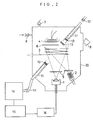
- a vacuum chamber 20 as shown in Fig. 2 incorporating an evaporation source 1 heated with electron beam, a Knudsen cell 2, a high-frequency working coil 3 for generating plasma and the like was evacuated to about 1 X 10 -8 Torr by means of a vacuum pump connected to an exhaust outlet 9 of the chamber 20. Thereafter, oxygen gas was introduced therein but only to around the coil 3 through a valve 8 up to 2 X 10 -4 Torr and which was made into plasma by being applied with Rf power (13.56 MHz, 200 W) by means of the coil 3.
- a thin film was formed on a substrate 4 (Corning 7059 glass) as heated to and maintained at 400 °C by simultaneously depositing Nb and Li vapors which were respectively produced from Nb (purity: 4N) disposed in the evaporation source 1 and from Li (purity: 4N) disposed in the Knudsen cell 2 by individually controlled heating, and which were then passed through the oxygen plasma atmosphere.
- Nb purity: 4N
- Li purity: 4N
- the deposition rate of Nb was fixed to 10 ⁇ /min. while that of Li was varied within the range of 10-30 ⁇ /min.
- the eventual thickness of the film was designed to be about 3000 ⁇ .
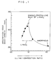
- Fig. 1 reveals the following facts:
- the Li-to-Nb composition ratio determines the absorption edge, and hence whether a film-forming condition is proper or not can be judged on the basis of whether the absorption edge of the obtained film falls within the range 310-320 nm, even if the film-forming conditions such as the deposition rates of Li and Nb are changed.
- An apparatus for preparing an LiNbO 3 was manufactured by providing the vacuum chamber of the former example with a visible-ultraviolet Spectrophotometer capable of measuring spectral characteristics in the visible-ultraviolet region on the basis of which a composition of an LiNbO 3 thin film being formed could be evaluated. Then, an LiNbO 3 thin film was prepared using the thus manufactured apparatus.
- FIG. 2 The schematic sectional view of the apparatus is shown in Fig. 2.
- an optical path 11 for spectrometry in which a monitor quartz substrate 13 and a quartz window 10 are disposed is provided for the vacuum chamber 20 described in the former example.
- the reference numeral 7 denotes a vacuum gauge.
- An oxygen plasma atmosphere was produced in the vacuum chamber 20 as in the same manner described in the former example. Then, Li placed in the Knudsen cell 2 was heated to 560 °C and emission current for the evaporation source 1 for Nb was set to 100 mA to render the evaporation states of Li and Nb constant. Shutters 5 for both of the evaporation source were opened to perform simultaneous deposition of Li and Nb on the monitor quartz substrate 13. During this monitoring deposition, light from a light source 12 was allowed to transmit through the quartz substrate 13 and the absorption edge of the thin film being formed was measured using a spectrometer 14 capable of measuring visible-ultraviolet region.
- the absorption edge could easily be specified from the shape of the spectrum.
- the measured absorption edge was 270 nm.
- Under control of a computer 15 output of a power controller 16 of the evaporation source 1 was increased for raising the emission current so that the absorption edge could fall within the range of about 310-320 nm which was the absorption edge range of an LiNbO 3 thin film of the stoichiometrical composition ratio. Consequently, when the emission current was 170 mA, the absorption edge of the thin film being monitored indicated 310 nm.
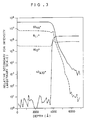
- Fig. 3 shows a composition distribution of Nb and Li of the thus formed thin film in terms of film-growing direction.
- the composition distribution in terms of film-growing direction was uniform and a relative secondary ion intensity ratio of Nb and Li agreed well to that of a single-crystalline bulk of LiNbO 3 .
- any evaporation means may be used in combination with the method of the present embodiments provided that the required deposition rate can be attained.
Landscapes
- Physics & Mathematics (AREA)
- General Physics & Mathematics (AREA)
- Chemical & Material Sciences (AREA)
- Analytical Chemistry (AREA)
- Optics & Photonics (AREA)
- Mathematical Physics (AREA)
- Health & Medical Sciences (AREA)
- Life Sciences & Earth Sciences (AREA)
- Engineering & Computer Science (AREA)
- Microelectronics & Electronic Packaging (AREA)
- Biochemistry (AREA)
- General Health & Medical Sciences (AREA)
- Immunology (AREA)
- Pathology (AREA)
- Investigating Or Analysing Materials By Optical Means (AREA)
- Crystals, And After-Treatments Of Crystals (AREA)
- Optical Modulation, Optical Deflection, Nonlinear Optics, Optical Demodulation, Optical Logic Elements (AREA)
Claims (12)
- Procédé d'évaluation d'un film mince de niobate de lithium, comprenant la mesure de la longueur d'onde de l'arête d'absorption d'un film mince de niobate de lithium et l'évaluation du rapport de composition lithium/niobium du film mince à partir de la longueur d'onde de l'arête d'absorption mesurée et d'une relation prédéterminée entre le rapport de composition et les valeurs de ladite longueur d'onde de l'arête d'absorption.
- Procédé selon la revendication 1, dans lequel la valeur mesurée de la longueur d'onde de l'arête d'absorption du film mince est comparée à ladite relation prédéterminée que l'on obtient à partir d'un échantillon, préparé au préalable, de film mince de niobate de lithium.
- Procédé selon la revendication 2, qui inclut l'étape de préparation dudit échantillon de film mince de niobate de lithium et l'établissement de ladite relation prédéterminée par mesure de son rapport de composition et de sa longueur d'onde de l'arête d'absorption.
- Procédé selon la revendication 1, dans lequel, si la valeur mesurée de la longueur d'onde de l'arête d'absorption du film mince se situe dans la gamme de 310 nm à 320 nm, on évalue le rapport de composition lithium/niobium du film mince à 1:1.
- Procédé selon la revendication 1, dans lequel le film mince est formé sur un substrat par pulvérisation cathodique ou plaquage ionique.
- Procédé selon la revendication 1, qui comprend aussi la formation dudit film mince de niobate de lithium sous forme d'un film contrôlé sur un substrat de contrôle dans la même atmosphère que celle utilisée pour former le film mince de niobate de lithium recherché sur un substrat par pulvérisation cathodique ou plaquage ionique et avant ou pendant la formation dudit film mince recherché.
- Appareil de préparation d'un film mince, comprenant un dispositif utilisant des sources de lithium et de niobium (1, 2) et fonctionnant pour former un film mince de niobate de lithium sur un substrat (4) en permettant de régler le rapport de composition lithium/niobium du film mince de niobate de lithium, et un dispositif d'évaluation comprenant une source de rayons ultraviolets (12), un substrat de contrôle (13) placé sur le trajet optique de la source lumineuse, un moyen (14) pour mesurer la longueur d'onde de l'arête d'absorption du film mince de niobate de lithium formé sur ledit substrat de contrôle, un moyen pour évaluer le rapport de composition lithium/niobium à partir de la longueur d'onde de l'arête d'absorption mesurée et de la relation prédéterminée entre le rapport de composition et les valeurs de ladite longueur d'onde de l'arête d'absorption, et un moyen pour régler ledit rapport selon le résultat de l'évaluation.
- Appareil selon la revendication 7, dans lequel un substrat de contrôle et le trajet optique du dispositif d'évaluation sont placés à l'intérieur du dispositif de formation du film.
- Appareil selon la revendication 7 ou 8, dans lequel le moyen de réglage est prévu pour régler le rapport de composition du film mince en formation, si la valeur d'évaluation dudit rapport de composition obtenu par le dispositif d'évaluation diffère de la valeur prédéterminée.
- Appareil selon l'une quelconque des revendications 7 à 9, dans lequel le dispositif de formation du film mince fonctionne par pulvérisation cathodique ou plaquage ionique.
- Procédé pour former un film mince de niobate de lithium en utilisant un procédé dans lequel il est possible de régler le rapport de composition Li/Nb, dans lequel ledit rapport de composition est évalué durant la formation du film par mesure de la longueur d'onde de l'arête d'absorption du film et détermination de la valeur dudit rapport à partir de la longueur d'onde mesurée et de la relation prédéterminée entre le rapport de composition et les valeurs de ladite longueur d'onde de l'arête d'absorption, et dans lequel ledit rapport est réglé en fonction du résultat de l'évaluation.
- Procédé pour former un film mince d'une matière donnée en utilisant un procédé dans lequel le rapport de composition entre au moins deux éléments constitutifs de la matière peut être réglé, dans lequel ledit rapport de composition est évalué durant la formation du film par mesure de la longueur d'onde de l'arête d'absorption du film et détermination de la valeur dudit rapport à partir de la longueur d'onde mesurée et de la relation prédéterminée entre le rapport de composition et les valeurs de ladite longueur d'onde de l'arête d'absorption, et dans lequel ledit rapport est réglé en fonction du résultat de l'évaluation.
Applications Claiming Priority (2)
| Application Number | Priority Date | Filing Date | Title |
|---|---|---|---|
| JP2114434A JPH049748A (ja) | 1990-04-27 | 1990-04-27 | ニオブ酸リチウム薄膜の評価方法およびその製造装置 |
| JP114434/90 | 1990-04-27 |
Publications (3)
| Publication Number | Publication Date |
|---|---|
| EP0454499A2 EP0454499A2 (fr) | 1991-10-30 |
| EP0454499A3 EP0454499A3 (en) | 1992-02-19 |
| EP0454499B1 true EP0454499B1 (fr) | 1996-11-27 |
Family
ID=14637628
Family Applications (1)
| Application Number | Title | Priority Date | Filing Date |
|---|---|---|---|
| EP91303850A Expired - Lifetime EP0454499B1 (fr) | 1990-04-27 | 1991-04-29 | Méthode pour évaluer une couche mince de lithium niobate et appareil pour le préparer |
Country Status (4)
| Country | Link |
|---|---|
| US (1) | US5128007A (fr) |
| EP (1) | EP0454499B1 (fr) |
| JP (1) | JPH049748A (fr) |
| DE (1) | DE69123283T2 (fr) |
Cited By (2)
| Publication number | Priority date | Publication date | Assignee | Title |
|---|---|---|---|---|
| US11316193B2 (en) | 2016-06-15 | 2022-04-26 | Ilika Technologies Limited | Lithium borosilicate glass as electrolyte and electrode protective layer |
| US11851742B2 (en) | 2018-08-29 | 2023-12-26 | Ilika Technologies Limited | Vapor deposition method for preparing an amorphous lithium borosilicate |
Families Citing this family (11)
| Publication number | Priority date | Publication date | Assignee | Title |
|---|---|---|---|---|
| US5253104A (en) * | 1992-09-15 | 1993-10-12 | At&T Bell Laboratories | Balanced optical amplifier |
| DE4236264C1 (fr) * | 1992-10-27 | 1993-09-02 | Fraunhofer-Gesellschaft Zur Foerderung Der Angewandten Forschung Ev, 80636 Muenchen, De | |
| JP3113141B2 (ja) * | 1993-12-28 | 2000-11-27 | シャープ株式会社 | 強誘電体結晶薄膜被覆基板、その製造方法及び強誘電体結晶薄膜被覆基板を用いた強誘電体薄膜デバイス |
| GB9700017D0 (en) * | 1997-01-02 | 1997-02-19 | Applied Vision Ltd | Substrate coating apparatus |
| US6951120B2 (en) * | 2002-03-19 | 2005-10-04 | Wisconsin Alumni Research Foundation | Machining of lithium niobate by laser ablation |
| CN100543456C (zh) * | 2007-07-19 | 2009-09-23 | 广州天赐高新材料股份有限公司 | 一种双草酸硼酸锂含量紫外分光光度测定法 |
| KR20130040228A (ko) * | 2010-07-09 | 2013-04-23 | 케이-스페이스 어소시에이츠 인코포레이티드 | 투명한 기판에 도포된 박막의 실시간 온도, 광대역 차, 막 두께, 및 표면 거칠기를 측정하는 방법 및 장치 |
| GB201400274D0 (en) | 2014-01-08 | 2014-02-26 | Ilika Technologies Ltd | Vapour deposition method for preparing amorphous lithium-containing compounds |
| GB201400276D0 (en) | 2014-01-08 | 2014-02-26 | Ilika Technologies Ltd | Vapour deposition method for fabricating lithium-containing thin film layered structures |
| GB201400277D0 (en) * | 2014-01-08 | 2014-02-26 | Ilika Technologies Ltd | Vapour deposition method for preparing crystalline lithium-containing compounds |
| WO2016057990A2 (fr) * | 2014-10-10 | 2016-04-14 | Orthobond, Inc. | Procede pour la detection et l'analyse de films de surface |
Family Cites Families (9)
| Publication number | Priority date | Publication date | Assignee | Title |
|---|---|---|---|---|
| US3734620A (en) * | 1971-04-01 | 1973-05-22 | Ibm | Multiple band atomic absorption apparatus for simultaneously measuring different physical parameters of a material |
| US3892490A (en) * | 1974-03-06 | 1975-07-01 | Minolta Camera Kk | Monitoring system for coating a substrate |
| US4140078A (en) * | 1974-03-16 | 1979-02-20 | Leybold Heraeus Gmbh & Co. Kg | Method and apparatus for regulating evaporating rate and layer build up in the production of thin layers |
| US3988232A (en) * | 1974-06-25 | 1976-10-26 | Matsushita Electric Industrial Co., Ltd. | Method of making crystal films |
| US4166784A (en) * | 1978-04-28 | 1979-09-04 | Applied Films Lab, Inc. | Feedback control for vacuum deposition apparatus |
| US4172020A (en) * | 1978-05-24 | 1979-10-23 | Gould Inc. | Method and apparatus for monitoring and controlling sputter deposition processes |
| WO1980000504A1 (fr) * | 1978-08-18 | 1980-03-20 | Nat Res Dev | Commande du depot de pellicule fine |
| JPS57161063A (en) * | 1981-03-31 | 1982-10-04 | Nippon Sheet Glass Co Ltd | Method and device for sticking metallic oxide film on substrate |
| DD262286A1 (de) * | 1987-07-15 | 1988-11-23 | Werk Fernsehelektronik Veb | Verfahren zur bestimmung der stickstoffkonzentration in gaas tief 1-xpx/gap - epitaxiescheiben |
-
1990
- 1990-04-27 JP JP2114434A patent/JPH049748A/ja active Pending
-
1991
- 1991-04-25 US US07/691,502 patent/US5128007A/en not_active Expired - Lifetime
- 1991-04-29 DE DE69123283T patent/DE69123283T2/de not_active Expired - Fee Related
- 1991-04-29 EP EP91303850A patent/EP0454499B1/fr not_active Expired - Lifetime
Cited By (2)
| Publication number | Priority date | Publication date | Assignee | Title |
|---|---|---|---|---|
| US11316193B2 (en) | 2016-06-15 | 2022-04-26 | Ilika Technologies Limited | Lithium borosilicate glass as electrolyte and electrode protective layer |
| US11851742B2 (en) | 2018-08-29 | 2023-12-26 | Ilika Technologies Limited | Vapor deposition method for preparing an amorphous lithium borosilicate |
Also Published As
| Publication number | Publication date |
|---|---|
| DE69123283D1 (de) | 1997-01-09 |
| DE69123283T2 (de) | 1997-03-27 |
| EP0454499A2 (fr) | 1991-10-30 |
| US5128007A (en) | 1992-07-07 |
| EP0454499A3 (en) | 1992-02-19 |
| JPH049748A (ja) | 1992-01-14 |
Similar Documents
| Publication | Publication Date | Title |
|---|---|---|
| EP0454499B1 (fr) | Méthode pour évaluer une couche mince de lithium niobate et appareil pour le préparer | |
| KR940007608B1 (ko) | 진공처리 장치 및 이를 이용한 성막장치와 성막방법 | |
| Adachi et al. | Sputtering preparation of ferroelectric PLZT thin films and their optical applications | |
| KR100860182B1 (ko) | 압전막을 제조하는데 사용하기 위한 방법, 반응성 스퍼터링 방법 및 압전 디바이스 제조 방법 | |
| CN112016676B (zh) | 一种神经网络模型预测的半导体薄膜工艺参数优化系统 | |
| Marsh et al. | Pulsed laser deposition of high quality LiNbO3 films on sapphire substrates | |
| US3620814A (en) | Continuous measurement of the thickness of hot thin films | |
| Mortet et al. | Aluminium nitride films deposition by reactive triode sputtering for surface acoustic wave device applications | |
| Okuyama et al. | Ferroelectric PbTiO3 thin films and their application | |
| US4560576A (en) | Method of coating optical components | |
| JPH0192375A (ja) | マイクロ波プラズマcvd法による機能性堆積膜形成装置 | |
| US4140078A (en) | Method and apparatus for regulating evaporating rate and layer build up in the production of thin layers | |
| CN110923674A (zh) | 一种拉曼光谱仪监控反馈式化学气相沉积系统及应用 | |
| JPH07283138A (ja) | シリコンへの炭素のレーザー蒸着による炭化シリコンの結晶学的整合フィルムの作成 | |
| Dogheche et al. | m-line spectroscopy for optical analysis of thick LiNbO 3 layers grown on sapphire substrates by radio-frequency multistep sputtering | |
| Antoine et al. | Growth processes of RF glow discharge deposited a-Si: H and a-Ge: H films | |
| WO2020005203A1 (fr) | Réglage de densité in situ pendant la fabrication de matériaux de film mince | |
| US20030082834A1 (en) | Non-contacting deposition control of chalcopyrite thin films | |
| Lim et al. | Rugate filters grown by plasma-enhanced chemical vapor deposition | |
| EP1854904A1 (fr) | Appareil de mesure des caractéristiques physiques du semi-conducteur | |
| Verardi et al. | Epitaxial piezoelectric PZT thin films obtained by pulsed laser deposition | |
| Krzesiński | A study of the effect of technological parameters of rf sputtering on the size of grains and the texture of thin ZnO films | |
| JPH07152007A (ja) | 直流電圧のドリフトが制御されている導波路型電気光学素子 | |
| Krishnakumar et al. | Characterization of ferroelectric thin film PLZT (9/65/35) on R-plane sapphire | |
| Das et al. | Microstructural, optical and electrical studies of sputtered epitaxial CdTe films |
Legal Events
| Date | Code | Title | Description |
|---|---|---|---|
| PUAI | Public reference made under article 153(3) epc to a published international application that has entered the european phase |
Free format text: ORIGINAL CODE: 0009012 |
|
| 17P | Request for examination filed |
Effective date: 19910524 |
|
| AK | Designated contracting states |
Kind code of ref document: A2 Designated state(s): DE FR GB |
|
| RIN1 | Information on inventor provided before grant (corrected) |
Inventor name: OKAMOTO, YASUNARI Inventor name: OHNO, HIROTAKA, NISHIYAMOTO Inventor name: MATSUNAGA, HIRONORI |
|
| PUAL | Search report despatched |
Free format text: ORIGINAL CODE: 0009013 |
|
| AK | Designated contracting states |
Kind code of ref document: A3 Designated state(s): DE FR GB |
|
| 17Q | First examination report despatched |
Effective date: 19940513 |
|
| GRAG | Despatch of communication of intention to grant |
Free format text: ORIGINAL CODE: EPIDOS AGRA |
|
| GRAH | Despatch of communication of intention to grant a patent |
Free format text: ORIGINAL CODE: EPIDOS IGRA |
|
| GRAH | Despatch of communication of intention to grant a patent |
Free format text: ORIGINAL CODE: EPIDOS IGRA |
|
| GRAA | (expected) grant |
Free format text: ORIGINAL CODE: 0009210 |
|
| AK | Designated contracting states |
Kind code of ref document: B1 Designated state(s): DE FR GB |
|
| ET | Fr: translation filed | ||
| REF | Corresponds to: |
Ref document number: 69123283 Country of ref document: DE Date of ref document: 19970109 |
|
| PLBE | No opposition filed within time limit |
Free format text: ORIGINAL CODE: 0009261 |
|
| STAA | Information on the status of an ep patent application or granted ep patent |
Free format text: STATUS: NO OPPOSITION FILED WITHIN TIME LIMIT |
|
| 26N | No opposition filed | ||
| REG | Reference to a national code |
Ref country code: GB Ref legal event code: IF02 |
|
| PGFP | Annual fee paid to national office [announced via postgrant information from national office to epo] |
Ref country code: FR Payment date: 20020410 Year of fee payment: 12 |
|
| PGFP | Annual fee paid to national office [announced via postgrant information from national office to epo] |
Ref country code: GB Payment date: 20020424 Year of fee payment: 12 |
|
| PGFP | Annual fee paid to national office [announced via postgrant information from national office to epo] |
Ref country code: DE Payment date: 20020508 Year of fee payment: 12 |
|
| PG25 | Lapsed in a contracting state [announced via postgrant information from national office to epo] |
Ref country code: GB Free format text: LAPSE BECAUSE OF NON-PAYMENT OF DUE FEES Effective date: 20030429 |
|
| PG25 | Lapsed in a contracting state [announced via postgrant information from national office to epo] |
Ref country code: DE Free format text: LAPSE BECAUSE OF NON-PAYMENT OF DUE FEES Effective date: 20031101 |
|
| GBPC | Gb: european patent ceased through non-payment of renewal fee | ||
| PG25 | Lapsed in a contracting state [announced via postgrant information from national office to epo] |
Ref country code: FR Free format text: LAPSE BECAUSE OF NON-PAYMENT OF DUE FEES Effective date: 20031231 |
|
| REG | Reference to a national code |
Ref country code: FR Ref legal event code: ST |