EP0454992A2 - Suppression des parasites électriques d'un circuit électronique - Google Patents
Suppression des parasites électriques d'un circuit électronique Download PDFInfo
- Publication number
- EP0454992A2 EP0454992A2 EP91104650A EP91104650A EP0454992A2 EP 0454992 A2 EP0454992 A2 EP 0454992A2 EP 91104650 A EP91104650 A EP 91104650A EP 91104650 A EP91104650 A EP 91104650A EP 0454992 A2 EP0454992 A2 EP 0454992A2
- Authority
- EP
- European Patent Office
- Prior art keywords
- transmission line
- frequency
- node
- suppression
- stub
- Prior art date
- Legal status (The legal status is an assumption and is not a legal conclusion. Google has not performed a legal analysis and makes no representation as to the accuracy of the status listed.)
- Pending
Links
Images



Classifications
-
- H—ELECTRICITY
- H01—ELECTRIC ELEMENTS
- H01P—WAVEGUIDES; RESONATORS, LINES, OR OTHER DEVICES OF THE WAVEGUIDE TYPE
- H01P1/00—Auxiliary devices
- H01P1/20—Frequency-selective devices, e.g. filters
- H01P1/201—Filters for transverse electromagnetic waves
- H01P1/202—Coaxial filters
Definitions
- the present invention relates to the suppression of electro-magnetic interference (EMI) emissions from an electronic circuit.
- EMI electro-magnetic interference
- resonant transmission lines are designed for the noise frequency to be suppressed and connected at specific points to force a low impedance for the radiation to be suppressed at that location.
- the specific points may include power buses where they are connected to circuit modules, or any location in a circuit, on a card or board having a noise frequency to be suppressed. If the selected point is in a DC power distribution system where a shorted transmission line cannot be used, an open transmission line is used. An open transmission line having a length of an odd number of quarter wavelengths from the end of the line creates a low impedance which effectively creates a short circuit at the frequencies of odd harmonics resonant at that quarter wavelength.
- any number of transmission line stubs can be paralleled without interaction.
- Parallel stubs may also be used to broaden the null as in a multi-pole filter. If there are several frequencies to be suppressed present, transmission lines can be chosen to short out the undesired ones. For a single basic clock frequency switching at digital rates, one lowest frequency, the fundamental frequency, will tend to predominate and all harmonics of that frequency will be present.
- a resonant transmission line tuned to the fundamental frequency will suppress the first, third, fifth and all higher odd harmonics.
- a second resonant transmission line tuned to the second harmonic will suppress the second, sixth, tenth and other odd multiples of the even harmonics. Where the chosen location is a node in a circuit, on a card or a board, the resonant transmission line is a shorted transmission line.
- the transmission line of the present invention can be of any form; concentric, parallel balanced, etc. It can be formed in stripline over a ground plane or stripline as a balanced parallel feed. If the point at which interference is to be suppressed is referenced to a ground or signal reference plane, a standard concentric transmission line, as shown herein, may be used. If suppression is to occur between two points that are both floating relative to the nearest frame or reference planes, a shielded balanced line is used so that there is less loss or radiation from the transmission stub itself.
- the low impedance created by the transmission line is resonant at specific frequencies with a very high Q, there could be a frequency sensitivity that would appear with physical variations in the fabricated assembly. Since a low impedance is created, additional parallel stubs can be used to broaden the null as in a multi-pole filter.
- the impedance of the transmission line is related to how good an open circuit is at the other end of the line, reflected back, as though the line characteristics impedance is the geometric mean between the low impedance created and the open circuit at the far end of the line. This impedance may be described by:
- Attenuation, or line loss, is generally dominated by series resistance.
- the attenuation factor can be approximated by:
- the low line impedance is created using higher capacitance on the line.
- This increase in capacitance also increases propagation time on the line by a factor of the square root of capacitance, thereby shortening the dimension required to achieve a quarter wavelength.
- the present invention provides for suppression of electrical interferences from a node of an electronic circuit using a resonant transmission line for the frequency of the interference to be suppressed which is attached to the node of the electronic circuit. Further, the resonant transmission line is an open transmission line.
- the present invention further provides an apparatus for the suppression of electrical interferences from a node of an electronic circuit using a resonant transmission line wherein the resonant transmission line is a shorted transmission line. Additionally, the present invention to provide a plurality of resonant transmission lines each tuned to a different frequency to provide a band of frequencies to be suppressed.
- the resonant transmission line includes a tuning element for tuning the frequency at which the transmission line resonates, preferably tuning element wherein the tuning element is a variable capacitor.
- Fig. 1 is a perspective drawing of a frame 10 on which are mounted a number of circuit modules 11, 12 and 13.
- the circuit modules 11, 12 and 13 are connected by means of an edge assembly 15 to bus bars 16, 17, 18 and 19.
- the bus bars 16 through 19 provide voltages at different potentials to circuits of the circuit modules 11, 12 and 13.
- the bus bars 16 through 19 are held in place by an insulating bracket member 20 such that the bus bars 16 through 19 are held rigidly in place and electrically insulated from one another.
- Stub members 22, 24 and 26 are open resonant transmission lines and are attached between the bus bars to provide a null on the bus bars at the resonant frequencies of the stubs 22, 24 and 26 for suppressing electrical interferences at those frequencies.
- Stub 22 is connected to a bracket member 30 which provides for connections between the open transmission line of the stub 22 to bus bars 16 and 17.
- Stub 24 is likewise connected between bus bars 17 and 18 by bracket member 32, and a bracket member 34 connects stub member 26 between bus bars 18 and 19.
- the actual connection between the bus bars 16 through 19 by corner member 15 to the circuits of circuit modules 11 through 13 are well known in the art.
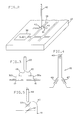
- Fig. 2 is a perspective drawing of a circuit board 36 which might be found, for instance, in one of the circuit modules 11 and 13.
- the circuit board 36 typically contains a clock circuit 38 whose switching frequencies cause electrical interferences to be radiated from the circuit 39 of the circuit board 36.
- a node 40 of the circuit 39 having the undesired electrical interference is located and a stub 42 is connected to the node 40 for suppression of the undesired electrical interference.
- the stub 42 may be a shorted transmission line, that is, a first conductor in the stub 42 is connected to the node 40, and a second conductor is connected to, for instance, the ground or singal reference plane 41 by a lead 43, as previously mentioned.
- Fig. 3 is a drawing of one of the stubs 22 of Fig. 1.
- the stub 22 is an open transmission line, and may be, for instance, a coaxial cable having its center conductor connected by a lead 45 to a portion of the bracket 30a which is connected to bus bar 16, and having its concentric shield connected by a lead 46 to a second portion 30b of the bracket member which in turn is connected to bus bar 17.
- the bracket portions 30a and 30b are electrically isolated from one another such that the bus bars 16 and 17 maintain their separate potentials.
- Fig. 4 is a schematic diagram of the stub 22 of Fig. 3.
- Inductance 47 represents the inductance of the bracket 30a and the lead 45
- the inductance 48 represents the inductance of the bracket 30b and its lead 46.
- a variable capacitor 49 may be added to the end of the stub 22 at its distal end, or the end opposite the end of the stub which is connected to the bracket member 30. Variable capacitor 49 may be used to tune the exact frequency at which the open transmission line of stub 22 resonates, thereby tuning to the frequency of the electrical interference to be suppressed.
- Fig. 5 is a schematic diagram of the stub 42 of Fig. 2 showing a variable capacitor 50 at the end of the stub 42 which is connected to the node 40.
- This configuration may be used when the transmission line of the stub is a shorted transmission line.
- the center conductor is shorted to the concentric shield, and the concentric shield is shorted to the circuit board at 41 by the lead 43.
- Fig. 6 shows one of the transmission line stubs 22 connected between the bus bars 16 and 17, and a second stub 60 also connected between the bus bars 16 and 17 by leads 62 and 64.
- the second stub 60 may be tuned to suppress even harmonics of the fundamental frequency of stub 22, or may be tuned to provide a band of suppression in the manner of a multi-pole filter.
- Fig. 7 is a graph showing the suppression of the fundamental and odd harmonics of electrical interference when a transmission line is tuned to the fundamental frequency.
- the transmission line is tuned to a fundamental frequency of 100 megahertz, and as shown, the odd harmonics of 300 megahertz and 500 megahertz would also be suppressed.
- Fig. 8 is a chart showing the suppression of frequencies of electrical interference when two transmission lines are used, one tuned to the fundamental frequency and one tuned to the even harmonics of the fundamental frequency.
- the fundamental frequency is 100 megahertz.
- the first transmission line suppresses the fundamental frequency of 100 megahertz and its odd harmonics of 300 and 500 megahertz.
- a second transmission line tuned to the even harmonics of the fundamental frequency would suppress electrical interferences of 200 megahertz and 600 megahertz.
- Fig. 9 is a chart of the suppression of electrical interferences when two lines having close resonant frequencies are used to suppress a band of electrical interferences between 80 and 125 megahertz.
Landscapes
- Physics & Mathematics (AREA)
- Electromagnetism (AREA)
- Control Of Motors That Do Not Use Commutators (AREA)
- Shielding Devices Or Components To Electric Or Magnetic Fields (AREA)
- Filters And Equalizers (AREA)
Applications Claiming Priority (2)
| Application Number | Priority Date | Filing Date | Title |
|---|---|---|---|
| US519528 | 1983-08-01 | ||
| US07/519,528 US5063362A (en) | 1990-05-04 | 1990-05-04 | Suppression of electrical interferences from an electronic circuit |
Publications (2)
| Publication Number | Publication Date |
|---|---|
| EP0454992A2 true EP0454992A2 (fr) | 1991-11-06 |
| EP0454992A3 EP0454992A3 (en) | 1991-11-21 |
Family
ID=24068696
Family Applications (1)
| Application Number | Title | Priority Date | Filing Date |
|---|---|---|---|
| EP19910104650 Pending EP0454992A3 (en) | 1990-05-04 | 1991-03-25 | Suppression of electrical interferences from an electronic circuit |
Country Status (3)
| Country | Link |
|---|---|
| US (1) | US5063362A (fr) |
| EP (1) | EP0454992A3 (fr) |
| JP (1) | JPH0575370A (fr) |
Families Citing this family (2)
| Publication number | Priority date | Publication date | Assignee | Title |
|---|---|---|---|---|
| DE102005033306B3 (de) * | 2005-07-16 | 2006-08-03 | Atmel Germany Gmbh | Monolithisch integrierte Schaltung mit integrierter Entstörvorrichtung |
| CN109508266B (zh) * | 2018-11-06 | 2022-01-21 | 晶晨半导体(上海)股份有限公司 | 抑制emi干扰的方法 |
Family Cites Families (10)
| Publication number | Priority date | Publication date | Assignee | Title |
|---|---|---|---|---|
| US1576667A (en) * | 1924-02-09 | 1926-03-16 | Joseph O Mauborgne | System for eliminating interference |
| US1939053A (en) * | 1932-07-21 | 1933-12-12 | Bell Telephone Labor Inc | Short wave transmission |
| US2176963A (en) * | 1937-12-28 | 1939-10-24 | Postal Telegraph Cable Co | Single line telegraph repeater |
| NL7314268A (nl) * | 1973-10-17 | 1975-04-21 | Philips Nv | Microgolfinrichting in microstripuitvoering. |
| JPS52122739A (en) * | 1976-04-07 | 1977-10-15 | Toyota Motor Corp | Preventing device for vehicle wire propagation noise |
| JPS58161515A (ja) * | 1982-03-19 | 1983-09-26 | Yagi Antenna Co Ltd | 帯域除去「ろ」波器 |
| JPS6290013A (ja) * | 1985-10-16 | 1987-04-24 | Fujitsu Ltd | トラツプ回路 |
| JPS63199508A (ja) * | 1987-02-13 | 1988-08-18 | Sharp Corp | 低雑音マイクロ波増幅回路 |
| FR2628571B1 (fr) * | 1988-03-11 | 1990-11-09 | Thomson Csf | Filtre coupe-bande hyperfrequence en technologie micro-bande |
| JPH0246001A (ja) * | 1988-08-08 | 1990-02-15 | Sharp Corp | インピーダンス整合回路 |
-
1990
- 1990-05-04 US US07/519,528 patent/US5063362A/en not_active Expired - Fee Related
-
1991
- 1991-03-07 JP JP3065351A patent/JPH0575370A/ja active Pending
- 1991-03-25 EP EP19910104650 patent/EP0454992A3/en active Pending
Also Published As
| Publication number | Publication date |
|---|---|
| JPH0575370A (ja) | 1993-03-26 |
| EP0454992A3 (en) | 1991-11-21 |
| US5063362A (en) | 1991-11-05 |
Similar Documents
| Publication | Publication Date | Title |
|---|---|---|
| KR100254866B1 (ko) | Vlsi 디바이스에 대한 필터링을 제공하는 서브-파워 플레인 | |
| US5278528A (en) | Air insulated high frequency filter with resonating rods | |
| US4970625A (en) | Integrated module handle and chassis bulkhead for reducing electromagnetic interference emissions from circuit modules | |
| JP2845210B2 (ja) | 電磁放射を低減するグランド構成 | |
| US5912597A (en) | Printed circuit board | |
| US4875025A (en) | Microstrip transmission line for coupling to a dielectric resonator | |
| US5285007A (en) | System for reducing the emission of high frequency electromagnetic waves from computer systems | |
| US6657291B1 (en) | Combined resistor-capacitor elements for decoupling in electronic packages | |
| US5063362A (en) | Suppression of electrical interferences from an electronic circuit | |
| GB2327301A (en) | Microwave intruder detector using printed antenna | |
| US7182644B2 (en) | Filtering electromagnetic interference from low frequency transmission lines at a device enclosure | |
| Ott | Controlling EMI by proper printed wiring board layout | |
| US6055164A (en) | System and method for attenuating induced EMI and power converter employing the same | |
| KR100323797B1 (ko) | 컴퓨터 시스템의 플러그-인 어댑터 카드로부터의 고주파 방출을 최소화시키기 위한 방법 | |
| Leferink | Reduction of printed circuit board radiated emission | |
| US4908735A (en) | Electronic apparatus reducing generation of electro magnetic interference | |
| KR100512738B1 (ko) | 인쇄회로기판 및 이를 사용하는 전자기기 | |
| BG51169A3 (bg) | Устройство за деактивиране на интегрални схеми по електрически път | |
| EP0331486A2 (fr) | Antenne | |
| KR100868928B1 (ko) | 전자 방사를 감소시키는 방법 및 장치 | |
| JPH0110957Y2 (fr) | ||
| JPS58123201A (ja) | マイクロ波回路の遮蔽構造 | |
| Eroglu | A practical comparison of cabling effects on radiated emissions | |
| JP2001244600A (ja) | 電子機器および電子機器の実装方法 | |
| JP3408376B2 (ja) | フィルタ回路 |
Legal Events
| Date | Code | Title | Description |
|---|---|---|---|
| PUAI | Public reference made under article 153(3) epc to a published international application that has entered the european phase |
Free format text: ORIGINAL CODE: 0009012 |
|
| PUAL | Search report despatched |
Free format text: ORIGINAL CODE: 0009013 |
|
| AK | Designated contracting states |
Kind code of ref document: A2 Designated state(s): DE FR GB |
|
| AK | Designated contracting states |
Kind code of ref document: A3 Designated state(s): DE FR GB |
|
| 17P | Request for examination filed |
Effective date: 19911219 |
|
| 18W | Application withdrawn |
Withdrawal date: 19920206 |
|
| 17Q | First examination report despatched |
Effective date: 19920316 |
|
| D18W | Application withdrawn (deleted) | ||
| STAA | Information on the status of an ep patent application or granted ep patent |
Free format text: STATUS: THE APPLICATION IS DEEMED TO BE WITHDRAWN |
|
| 18D | Application deemed to be withdrawn |
Effective date: 19920728 |
|
| D18W | Application withdrawn (deleted) | ||
| K1C3 | Correction of patent application (complete document) published |
Effective date: 19911106 |