EP0455233A2 - Flüssigkristall-Anzeigevorrichtung mit Treiberschaltkreis - Google Patents
Flüssigkristall-Anzeigevorrichtung mit Treiberschaltkreis Download PDFInfo
- Publication number
- EP0455233A2 EP0455233A2 EP91107041A EP91107041A EP0455233A2 EP 0455233 A2 EP0455233 A2 EP 0455233A2 EP 91107041 A EP91107041 A EP 91107041A EP 91107041 A EP91107041 A EP 91107041A EP 0455233 A2 EP0455233 A2 EP 0455233A2
- Authority
- EP
- European Patent Office
- Prior art keywords
- substrate
- display device
- driving circuit
- crystal display
- liquid
- Prior art date
- Legal status (The legal status is an assumption and is not a legal conclusion. Google has not performed a legal analysis and makes no representation as to the accuracy of the status listed.)
- Granted
Links
Images


Classifications
-
- G—PHYSICS
- G02—OPTICS
- G02F—OPTICAL DEVICES OR ARRANGEMENTS FOR THE CONTROL OF LIGHT BY MODIFICATION OF THE OPTICAL PROPERTIES OF THE MEDIA OF THE ELEMENTS INVOLVED THEREIN; NON-LINEAR OPTICS; FREQUENCY-CHANGING OF LIGHT; OPTICAL LOGIC ELEMENTS; OPTICAL ANALOGUE/DIGITAL CONVERTERS
- G02F1/00—Devices or arrangements for the control of the intensity, colour, phase, polarisation or direction of light arriving from an independent light source, e.g. switching, gating or modulating; Non-linear optics
- G02F1/01—Devices or arrangements for the control of the intensity, colour, phase, polarisation or direction of light arriving from an independent light source, e.g. switching, gating or modulating; Non-linear optics for the control of the intensity, phase, polarisation or colour
- G02F1/13—Devices or arrangements for the control of the intensity, colour, phase, polarisation or direction of light arriving from an independent light source, e.g. switching, gating or modulating; Non-linear optics for the control of the intensity, phase, polarisation or colour based on liquid crystals, e.g. single liquid crystal display cells
- G02F1/133—Constructional arrangements; Operation of liquid crystal cells; Circuit arrangements
- G02F1/1333—Constructional arrangements; Manufacturing methods
- G02F1/1345—Conductors connecting electrodes to cell terminals
- G02F1/13452—Conductors connecting driver circuitry and terminals of panels
-
- G—PHYSICS
- G09—EDUCATION; CRYPTOGRAPHY; DISPLAY; ADVERTISING; SEALS
- G09G—ARRANGEMENTS OR CIRCUITS FOR CONTROL OF INDICATING DEVICES USING STATIC MEANS TO PRESENT VARIABLE INFORMATION
- G09G3/00—Control arrangements or circuits, of interest only in connection with visual indicators other than cathode-ray tubes
- G09G3/20—Control arrangements or circuits, of interest only in connection with visual indicators other than cathode-ray tubes for presentation of an assembly of a number of characters, e.g. a page, by composing the assembly by combination of individual elements arranged in a matrix no fixed position being assigned to or needed to be assigned to the individual characters or partial characters
- G09G3/34—Control arrangements or circuits, of interest only in connection with visual indicators other than cathode-ray tubes for presentation of an assembly of a number of characters, e.g. a page, by composing the assembly by combination of individual elements arranged in a matrix no fixed position being assigned to or needed to be assigned to the individual characters or partial characters by control of light from an independent source
- G09G3/36—Control arrangements or circuits, of interest only in connection with visual indicators other than cathode-ray tubes for presentation of an assembly of a number of characters, e.g. a page, by composing the assembly by combination of individual elements arranged in a matrix no fixed position being assigned to or needed to be assigned to the individual characters or partial characters by control of light from an independent source using liquid crystals
- G09G3/3611—Control of matrices with row and column drivers
- G09G3/3674—Details of drivers for scan electrodes
- G09G3/3677—Details of drivers for scan electrodes suitable for active matrices only
-
- G—PHYSICS
- G09—EDUCATION; CRYPTOGRAPHY; DISPLAY; ADVERTISING; SEALS
- G09G—ARRANGEMENTS OR CIRCUITS FOR CONTROL OF INDICATING DEVICES USING STATIC MEANS TO PRESENT VARIABLE INFORMATION
- G09G3/00—Control arrangements or circuits, of interest only in connection with visual indicators other than cathode-ray tubes
- G09G3/20—Control arrangements or circuits, of interest only in connection with visual indicators other than cathode-ray tubes for presentation of an assembly of a number of characters, e.g. a page, by composing the assembly by combination of individual elements arranged in a matrix no fixed position being assigned to or needed to be assigned to the individual characters or partial characters
- G09G3/34—Control arrangements or circuits, of interest only in connection with visual indicators other than cathode-ray tubes for presentation of an assembly of a number of characters, e.g. a page, by composing the assembly by combination of individual elements arranged in a matrix no fixed position being assigned to or needed to be assigned to the individual characters or partial characters by control of light from an independent source
- G09G3/36—Control arrangements or circuits, of interest only in connection with visual indicators other than cathode-ray tubes for presentation of an assembly of a number of characters, e.g. a page, by composing the assembly by combination of individual elements arranged in a matrix no fixed position being assigned to or needed to be assigned to the individual characters or partial characters by control of light from an independent source using liquid crystals
- G09G3/3611—Control of matrices with row and column drivers
- G09G3/3674—Details of drivers for scan electrodes
- G09G3/3681—Details of drivers for scan electrodes suitable for passive matrices only
-
- G—PHYSICS
- G09—EDUCATION; CRYPTOGRAPHY; DISPLAY; ADVERTISING; SEALS
- G09G—ARRANGEMENTS OR CIRCUITS FOR CONTROL OF INDICATING DEVICES USING STATIC MEANS TO PRESENT VARIABLE INFORMATION
- G09G3/00—Control arrangements or circuits, of interest only in connection with visual indicators other than cathode-ray tubes
- G09G3/20—Control arrangements or circuits, of interest only in connection with visual indicators other than cathode-ray tubes for presentation of an assembly of a number of characters, e.g. a page, by composing the assembly by combination of individual elements arranged in a matrix no fixed position being assigned to or needed to be assigned to the individual characters or partial characters
- G09G3/34—Control arrangements or circuits, of interest only in connection with visual indicators other than cathode-ray tubes for presentation of an assembly of a number of characters, e.g. a page, by composing the assembly by combination of individual elements arranged in a matrix no fixed position being assigned to or needed to be assigned to the individual characters or partial characters by control of light from an independent source
- G09G3/36—Control arrangements or circuits, of interest only in connection with visual indicators other than cathode-ray tubes for presentation of an assembly of a number of characters, e.g. a page, by composing the assembly by combination of individual elements arranged in a matrix no fixed position being assigned to or needed to be assigned to the individual characters or partial characters by control of light from an independent source using liquid crystals
- G09G3/3611—Control of matrices with row and column drivers
- G09G3/3685—Details of drivers for data electrodes
- G09G3/3688—Details of drivers for data electrodes suitable for active matrices only
-
- G—PHYSICS
- G09—EDUCATION; CRYPTOGRAPHY; DISPLAY; ADVERTISING; SEALS
- G09G—ARRANGEMENTS OR CIRCUITS FOR CONTROL OF INDICATING DEVICES USING STATIC MEANS TO PRESENT VARIABLE INFORMATION
- G09G3/00—Control arrangements or circuits, of interest only in connection with visual indicators other than cathode-ray tubes
- G09G3/20—Control arrangements or circuits, of interest only in connection with visual indicators other than cathode-ray tubes for presentation of an assembly of a number of characters, e.g. a page, by composing the assembly by combination of individual elements arranged in a matrix no fixed position being assigned to or needed to be assigned to the individual characters or partial characters
- G09G3/34—Control arrangements or circuits, of interest only in connection with visual indicators other than cathode-ray tubes for presentation of an assembly of a number of characters, e.g. a page, by composing the assembly by combination of individual elements arranged in a matrix no fixed position being assigned to or needed to be assigned to the individual characters or partial characters by control of light from an independent source
- G09G3/36—Control arrangements or circuits, of interest only in connection with visual indicators other than cathode-ray tubes for presentation of an assembly of a number of characters, e.g. a page, by composing the assembly by combination of individual elements arranged in a matrix no fixed position being assigned to or needed to be assigned to the individual characters or partial characters by control of light from an independent source using liquid crystals
- G09G3/3611—Control of matrices with row and column drivers
- G09G3/3685—Details of drivers for data electrodes
- G09G3/3692—Details of drivers for data electrodes suitable for passive matrices only
-
- H—ELECTRICITY
- H10—SEMICONDUCTOR DEVICES; ELECTRIC SOLID-STATE DEVICES NOT OTHERWISE PROVIDED FOR
- H10W—GENERIC PACKAGES, INTERCONNECTIONS, CONNECTORS OR OTHER CONSTRUCTIONAL DETAILS OF DEVICES COVERED BY CLASS H10
- H10W90/00—Package configurations
-
- G—PHYSICS
- G09—EDUCATION; CRYPTOGRAPHY; DISPLAY; ADVERTISING; SEALS
- G09G—ARRANGEMENTS OR CIRCUITS FOR CONTROL OF INDICATING DEVICES USING STATIC MEANS TO PRESENT VARIABLE INFORMATION
- G09G2310/00—Command of the display device
- G09G2310/02—Addressing, scanning or driving the display screen or processing steps related thereto
- G09G2310/0264—Details of driving circuits
- G09G2310/0289—Details of voltage level shifters arranged for use in a driving circuit
Definitions
- the present invention relates to a liquid crystal display device in which a driving circuit for supplying driving signals to at least one of the opposing electrodes is installed on at least one substrate of liquid crystal display cells.
- a matrix-type liquid crystal display device for displaying television pictures comprises, an electrode for display formed on a pair of opposed glass substrates, and a liquid crystal layer sandwiched between a pair of substrates.
- the liquid crystal display device includes the simple matrix type and the TFT (thin film transistor) active matrix type.
- TFT thin film transistor
- TFT-active-matrix-type liquid-crystal display device many pixel electrodes and thin film transistors (TFTs) for selecting each pixel electrode are arranged in rows and columns on one glass substrate and opposing electrodes are formed on the other glass substrate.
- TFTs thin film transistors
- Figs. 1 and 2 show a simple-matrix-type liquid-crystal display device having the existing display driving circuit.
- a pair of glass substrates 1 and 2 faced at the both sides of a liquid crystal layer LC are bonded through the frame-shaped sealing member 3 enclosing the liquid crystal sealing area.
- Many striped scanning electrodes 4 transparent electrodes
- Many striped signal electrodes 5 orthogonal to the scanning electrodes 4 are arranged in parallel on the other glass substrate 2 (lower substrate in the drawing).
- orientation films 6a and 6b are formed on the surface where electrodes of the both substrates 1 and 2 are formed.
- the signal electrodes 5 are separated at the middle in the longitudinal direction to individually drive each signal electrode 5 so that the display driving duty ratio will be decreased.
- scanning driving circuit elements 7a are installed on one end of the glass substrate 1.
- signal driving circuit elements devices 7b are installed on the both ends of the other glass substrate 2 respectively.
- the output terminal of each scanning driving circuit element 7a is installed by solder or the like on the end of a driving circuit connecting lead wire 4a which is extended from the end of each scanning electrode 4 and arranged on the surface of the glass substrate 1.
- the output terminal of each signal driving circuit element 7b is installed by solder or the like on the end of a driving circuit connecting lead wire 5a which is extended from the end of each signal electrode 5 and arranged on the surface of the glass substrate 2.
- Numeral 8a is an external-circuit connecting wire arranged on the surface of the glass substrate 1 and numeral 8b is an external-circuit connecting wire arranged on the surface of the glass substrate 2.
- the input terminal of the driving circuit elements 7a and 7b are connected by solder or the like with the external-circuit connecting wires 8a and 8b respectively.
- the driving circuit elements 7a and 7b use an IC chip in which many MOS-type transistors are formed on a single-crystal silicon substrate.
- the scanning and signal display driving circuits comprise several driving circuit elements (IC chip) 7a and 7b respectively.
- the existing active-matrix-type liquid-crystal display device includes two types: one is the type using a single crystal silicon substrate as each of the pair of substrates of the liquid crystal cell on which single-crystal MOS-type transistors made of single crystal silicon are formed as the selecting transistor for selecting a pixel electrode, and the other is the TFT active-matrix-type using thin film transistors (TFTs) as the selecting transistor for selecting a pixel electrode.
- TFTs thin film transistors
- the active-matrix-type liquid-crystal display device using the single-crystal MOS-type transistor uses a silicon substrate made of single crystal silicon as either substrate on which the MOS-type selecting transistors are formed.
- Each pixel electrodes of the active-matrix-type liquid-crystal display device are connected to the source electrode of each selecting transistor on the silicon substrate.
- the gate electrode and drain electrode of each selecting transistor are connected to many scanning lines and data lines which are orthogonally formed on the silicon substrate.
- TFT active-matrix-type liquid-crystal display device using thin film transistors
- many scanning lines and many data lines orthogonal to the scanning lines are formed on a glass substrate.
- a gate electrode, gate insulting film, semiconductor layer comprising amorphous silicon, and selecting transistor electrodes are formed on each intersection of the scanning and data lines.
- the gate electrode and drain electrode of each selecting thin-film transistor are connected to the scanning line and data line respectively, and the source electrode is connected to the pixel electrode formed on the glass substrate.
- opposing electrodes are formed on the opposing glass substrates.
- the display driving circuit comprises many single-crystal MOS-type transistors for driver formed on the periphery of line lead-out portion on the silicon substrate.
- the scanning and signal display driving circuits are composed of several driving circuit elements consisting of IC chip respectively and each driving circuit element is installed on the periphery of either glass substrate forming the pixel electrodes and the thin film transistors for selectively driving them.
- the terminal of each scanning driving circuit element is connected to the lead wire extended from the scanning line (gate line) connecting with the gate electrode of the thin film transistor for selectively driving pixel electrodes.
- the terminal of each signal driving circuit element is connected to the lead wire extended from the data line connecting with the drain electrode of the thin film transistor.
- the display driving circuit of the above existing liquid-crystal display device using IC chip is configured by installing several driving circuit elements consisting of IC chip on the glass substrate where display electrodes are formed, each of the above driving circuit elements must be connected to each lead wire arranged on the glass substrate. Therefore, it is complicated to manufacture the liquid-crystal display device.
- the operation speed of the display driving circuit is high because the transistors for selecting pixel electrodes and for driver use the single-crystal MOS-type transistor.
- the liquid-crystal display device manufacturing cost is very high because high-purity single-crystal silicon substrate should be used for the substrate.
- the TFT active-matrix-type liquid-crystal display device can use inexpensive and large-area glass substrate because the transistors for selecting pixel electrodes and for driver use a thin film transistor. Therefore, the liquid-crystal display device manufacturing cost can greatly be decreased. Moreover, it is possible to manufacture a large screen.
- the display driving circuit of the TFT active-matrix-type liquid-crystal display device is configured with thin film transistors using amorphous silicon as semiconductor, high-speed display driving cannot be made because the operation speed of the display driving circuit decreases.
- the thin film transistor using polycrystal silicon for the semiconductor layer it is preferable to use the thin film transistor using polycrystal silicon for the semiconductor layer. Because the thin film transistor using polycrystal silicon for the semiconductor layer has higher operation speed than the transistor using amorphous silicon, the operation speed of the display driving circuit can be improved.
- the substrate should be made of heat-resistant substrate capable of standing the high temperature.
- the existing TFT active-matrix-type liquid-crystal display device comprises thin film transistors for driver in which the display driving circuit is made at the end of the line lead-out portion of either glass substrate where the pixel electrode selecting thin-film transistors and pixel electrodes are formed. Therefore, to use the thin film transistor for driver using polycrystal silicon for the semiconductor layer, the above glass substrate must be made of heat-resistant glass such as quartz glass. Because the heat-resistant glass is much expensive compared with normal glass (e.g, soda-lime glass coated thereon with silicon dioxide film), the liquid-crystal display device manufacturing cost increases when the heat-resistant glass is used for the above glass substrate.
- the present invention is made in view of the above situation and it is an object of the present invention to provide liquid-crystal display devices which have display driving circuit and can easily be manufactured at a low cost.
- the liquid-crystal display device of this invention has: a first substrate on which a plurality of first electrodes are arrayed; a plurality of signal supplying lines which are electrically connected with the plurality of first electrodes, extended to the periphery of the first substrate, and formed on the first substrate so that a terminal portion will be provided with at least one end of the first electrode; a second substrate disposed to be separated from the first substrate at a predetermined gap and having at least one second electrode arranged to oppose the first electrodes; a sealing member arranged to enclose the area where the plurality of first electrodes inside the terminal portion on the first substrate are arrayed, and bonding the first substrate with the second substrate; a liquid crystal material sealed in the area enclosed by the sealing member for the first and second substrates; a heat-resistant sub-substrate; a driving circuit block in which an input terminal for display control signal supplied from the outside, a driving circuit which is formed by connecting a plurality of thin-film transistors using semiconductor having crystal structure
- a liquid-crystal display device having a display driving circuit can be manufactured only by installing each output terminal arranging the driver elements at its one end on each driving circuit connecting terminal at the terminal arranged portion of the glass substrate. Therefore, it is easy to manufacture the liquid-crystal display device compared with the existing liquid-crystal display device in which the display driving circuit is configured by installing a plurality of driving circuit elements comprising IC chip on the glass substrate forming electrodes for display one by one.
- the display driving circuit comprising the thin-film transistor is less expensive than the IC chip obtained by forming many MOS-type transistors on a single-crystal silicon substrate, the display driving circuit cost can also greatly be decreased.
- the driving circuit of the driver element is configured by the thin film transistor using polycrystal-silicon semiconductor.
- the thin film transistor using the polycrystal-silicon semiconductor has higher operation speed than the thin film transistor using amorphous-silicon semiconductor. Therefore, the display driving circuit of the driver element can be operated at an adequately high speed as the display driving circuit of liquid-crystal display device.
- the substrate of driver element should use heat-resistant glass substrate in order to configure the display driving circuit of the driver element by the thin-film transistor using polycrystal-silicon semiconductor.
- the substrate of driver element can use at least a small strip substrate with the length corresponding to the entire terminal arranged area of the glass substrate formed on the electrode for display. Therefore, the liquid-crystal display device manufacturing cost can be decreased because only a small amount of expensive heat-resistant glass is necessary and the large-area glass substrate for forming electrodes for display can be made by inexpensive normal glass substrate requiring no heat resistance.
- Figs. 3 and 4 show the configuration of the TFT active-matrix-type liquid-crystal display device of this embodiment, in which numerals 101 and 102 are a pair of glass substrates faced at the both sides of the liquid crystal layer LC. These glass substrates 101 and 102 are made of normal glass substrate such as soda-lime glass coated thereon with silicon dioxide film. This pair of glass substrates 101 and 102 are bonded through the frame-shaped sealing member 103 enclosing the liquid crystal sealing area.
- the selecting TFT 6 as shown in Fig.
- the gate electrode 108 is made by laminating the gate electrode 108 connecting with the scanning line 104 arranged on the glass substrate 101, the gate insulating film 109 covering the gate electrode 108 and the scanning line 104, and the amorphous silicon semiconductor layer 110 formed on the gate insulating film 109 by facing with the gate electrode 108.
- a blocking layer 111 comprising an insulating film is formed at the center of the semiconductor layer 110 to form a channel, and the source electrode 112 and drain electrode 113 are stacked at the both sides of the semiconductor layer 110 through a contact layer 114 comprising n+-type semiconductor made by doping impurities.
- the drain electrode 113 is connected to the data line 5 arranged on the gate insulating film 109 and the source electrode 112 is connected to the pixel electrode 107.
- the opposing electrode 115 which opposes each of the pixel electrode 107 is formed on the other glass substrate (upper substrate in the drawing).
- the orientation films 116 and 117 are formed on the electrode forming surface of the both glass substrates 101 and 102 respectively.
- Each scanning line 104 and each data line 105 arranged on the glass substrate 101 are extended to one end and side of the glass substrate 101.
- the scanning driver element 118 is installed on the periphery of the scanning-line lead-out portion of the glass substrate 101 and the data driver element 119 is installed on the periphery of the data-line lead-out portion.
- driver elements 118 and 119 respectively form many thin-film transistors 120a and 121a (hereinafter referred to as TFT for driver) using polycrystal silicon as the semiconductor layer on the substrates 118a and 119a comprising heat-resistant glass such as quartz glass and the display driving circuits 120 and 121 are formed.
- TFTs for driver 120a and 121a have the same structure as the pixel selecting transistor shown in Fig. 6, which are formed by stacking the gate electrode, gate insulating film, polycrystal-silicon semiconductor layer opposing the gate electrode through the gate insulating film, source electrode, and drain electrode.
- the polycrystal-silicon semiconductor layer is made by polymerizing the deposited layer of amorphous silicon at a high temperature. Therefore, the substrates 118a and 119a should be made of heat-resistant glass capable of standing the heat treatment to polymerize the amorphous silicon.
- the driver elements 118 and 119 should be made of a strip element slightly longer than the line terminal arranged area at the scanning- and data-line lead-out ends of the glass substrate 101, which are installed on the line lead-out end of the glass substrate 101 by connecting output terminals 120a and 121a extended from the display driving circuit 120 and 121 to one side of the substrates 118a and 119a with the terminal portion 104a, 105a of each scanning line 104 and each data line 105 by solder or conductive anisotropic adhesive.
- the driver elements 118 and 119 and the glass substrate 101 are secured by the driver element securing resin 125 filled up between the elements and the glass substrate.
- Several input terminals 122 and 123 are formed on one end of the substrates 118a and 119a of the driver elements 118 and 119 respectively, which are connected with the external-circuit connecting wires 126 arranged on the corner of the glass substrate 101 by solder or the like.
- Fig. 7 is a block diagram of the display driving circuit 121 formed on the substrate 119a.
- the display driving circuit 121 comprises shift registers 127 of stages equal to the number of data lines of the liquid-crystal display device and level shifters 128 of stages equal to the number of the shift registers 127.
- the shift register 127 sequentially takes in the binary display data signal S D input from an external circuit synchronously with the shift clock Sc1.
- the display data for one scanning line taken in the final stage of the shift register 127 is sent from the shift register 127 to the level shifter 128 synchronously with the synchronizing clock Sc2 (scanning timing signal) input to the level shifter 128 from the external circuit.
- the level shifter 128 converts the display data for one scanning line into ON-level (high level) and OFF-level (low level) driving signals corresponding to the voltage V of the power source (binary power source) and outputs the signals to each data line 5.
- the level shifter 128 has a parallel-connection circuit of the inverter circuit shown in Fig. 8 and a holding circuit (not illustrated) for reading or outputting the display data sent from the shift register 127 synchronously with the synchronizing clock.
- the supply voltage V DD is applied to the drain electrode and inverters of several stages (e.g. four stages) comprising a load transistor T 1a made of TFT shorted between the drain and gate electrodes and a driver transistor T 2a made of TFT whose drain electrode is connected to the source electrode of the load transistor T 1a and whose source electrode is grounded are connected in parallel.
- the input terminal 128a is connected to the gate electrode of the driver transistor T 2a at the first stage and the drain electrode of the driver transistor T 2a is connected to the gate electrode of the driver transistor T 2a at the second stage as the output terminal of the first-stage inverter.
- drain electrode of the second-stage driver transistor T 2b is connected to the gate electrode of the third-stage driver transistor T 2c , the drain electrode of the third-stage driver transistor T 2c to the gate electrode of the fourth-stage driver transistor T 2d , and the drain electrode of the fourth-stage driver transistor T 2b to the drain line 105 or gate line 104 as the output terminal 128b of the inverter circuit.
- the display driving circuit 120 formed on the substrate 118a comprises, though not illustrated, shift registers of stages equal to the number of scanning lines of the liquid-crystal display device and level shifters of stages equal to the number of the shift registers similarly to the display driving circuit 121 of the data driver element 119.
- the display driving circuit 120 of the scanning driver element 118 sequentially outputs ON signal (gate signal to turn on the pixel selecting TFT 6) to each scanning line 104.
- ON signal gate signal to turn on the pixel selecting TFT 6
- the basic operations are the same as those of the display driving circuit 121 of the data-side driver element 119 except the fact that scanning-line selecting signal is input to the shift register instead of display data signal.
- the operation speed of the display driving circuits 120 and 121 of the scanning driver element 118 and data driver element 119 can be improved because they are configured by the driver TFTs 120a and 121a having a high operation speed using polycrystal silicon for the semiconductor layer.
- the driver TFTs 120a and 121a composing the display driving circuits 120 and 121 are formed on the substrates 118a and 119a which are different from the glass substrate 101 where the selecting TFT 106 and pixel electrode 107 are formed.
- the driver elements 118 and 119 composing the display driving circuits 120 and 121 are installed on the line lead-out end of the glass substrate 101 forming the pixel selecting TFT 106 and pixel electrode 107 and the pixel selecting TFT 106 uses amorphous silicon for the semiconductor layer. Therefore, the glass substrate 101 forming the pixel selecting TFT 106 and pixel electrode 107 can be made of normal glass (e.g.
- the substrates 118a and 119a of the driver elements 118 and 119 which should be made of heat-resistant glass such as quartz glass only require a substrate with the minimum area capable of forming the display driving circuits 120 and 121. Therefore, consumption of the expensive heat-resistant glass can be minimized and the liquid-crystal display device manufacturing cost can be decreased.
- the liquid-crystal display device uses glass for the substrates 118a and 119a of the driver elements 118 and 119 and for the substrate 101 forming the selecting TFT 106 and pixel electrode 107.
- the substrates 118a and 119a and the substrate 101 have almost same thermal expansion coefficient though they are different in heat resistance. Therefore, though the driver elements 118 and 119 made by forming display driving circuits 120 and 121 on the substrates 118a and 119a different from the glass substrate 101 are installed on the glass substrate 101 on which the pixel selecting TFT 106 and the pixel electrode 107 are formed, the driver elements 118 and 119 are not separated from the glass substrate 101 due to expansion or contraction caused by temperature change.
- the scanning driver element 118 and the data driver element 119 are made of a strip element slightly longer than the length of the line terminal arranged area at the scanning- and data-line lead-out ends of the glass substrate 101 where the pixel selecting TFT 106 and the pixel electrode 107 are formed.
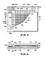
- Figs. 9 and 10 show the configuration of the liquid-crystal display device of the second embodiment of the present invention.
- the liquid-crystal display device of the second embodiment is the simple matrix type.
- numerals 201 and 202 are a pair of glass substrates opposed at the both sides of the liquid crystal layer LC and the glass substrates 201 and 202 should be made of normal glass such as soda-lime glass coated thereon with silicon dioxide film where silicon dioxide film is formed on the surface of soda-lime glass.
- This pair of glass substrates 201 and 202 are bonded through the frame-shaped sealing member 203 enclosing the liquid crystal sealing area.
- a plurality of striped scanning electrodes (transparent electrodes) 204 are formed in parallel on the glass substrate 201 (upper substrate in the drawing) of the pair of glass substrates 201 and 202, and a plurality of striped signal electrodes (transparent electrodes) orthogonal to the scanning electrodes 204 are formed in parallel on the glass substrate 202 (lower substrate in the drawing).
- the orientation films 206a and 206b are formed on the electrode forming surface of the substrates 201 and 202 respectively.
- the signal electrodes 205 are disconnected at the middle of the longitudinal length so that each signal electrode 205 will independently be driven in order to decrease the display driving duty ratio.
- each scanning electrode 204 formed on the glass substrate 201 is extended to the terminal arranged portion at the end of the glass substrate 101 to form the scanning driving circuit connecting terminal 204a.
- the end of each signal electrode 205 formed on the substrate 202 is extended to the terminal arranged portion at the both ends of the glass substrate 202 to form the signal driving circuit connecting terminal 205a.
- Each scanning driving circuit connecting terminal 204a is arranged in one line along the terminal arranged portion of the glass substrate 201 and each signal driving circuit connecting terminal 20a is arranged in one line along each terminal arranged portion of the glass substrate 202.
- numeral 220 is a scanning driver element installed at the terminal arranged portion of the glass substrate 201 and numeral 221 is a signal driver element installed on each terminal arranged portion of the glass substrate 202.
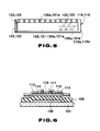
- the driver elements 220 and 221, as shown in Figs. 9 and 10, are made by forming many thin-film transistors 224a and 225a using polycrystal silicon for the semiconductor layer (hereafter referred to as driver TFT) on the strip substrates 222 and 223 slightly longer than the terminal arranged area at the terminal arranged end of the glass substrate 202 to configure the scanning driving circuit 224 and signal display driving circuit 225.
- the driver TFT 224a and 225a has the same structure as that in Fig. 6, which is configured by stacking a gate electrode, gate insulating film, and polycrystal-silicon semiconductor layer opposing the gate electrode through the gate insulating film, source electrode, and drain electrode.
- the polycrystal-silicon semiconductor layer is made by polymerizing the deposited layer of amorphous silicon at a high temperature. Therefore, the substrates 222 and 223 should be made of heat-resistant glass such as quartz glass capable of standing heat treatment to polymerize the amorphous silicon.
- the scanning driver element 220 is installed on the terminal arranged portion of the glass substrate 201 by connecting each output terminal 224a extended from the driving circuit 224 to one end of the substrate 222 to each scanning driving circuit connecting terminal 204a on the glass substrate 201 where the scanning electrode 204 is formed.
- Each signal driver element 221 is installed on each terminal arranged portion of the glass substrate 202 by connecting each output terminal 225a extended from the display driving circuit 225 to one end of the glass substrate 202 where the signal electrode 205 is formed to each signal driving circuit connecting terminal 205a on the glass substrate 202.
- the output terminals 224a and 224b of the scanning and signal driver elements 220 and 221 are arranged at the pitch corresponding to the arrangement pitch of the driving circuit connecting terminals 204a and 205a, and the output terminal 224a is connected to the driving circuit connecting terminal 205a by solder 226 or the like.
- numeral 227 is driver element securing resin filled up between the driver element 220 and the glass substrate 201 and between the driver element 221 and the glass substrate 202.
- a plurality of input terminals 224b and 225b extended from the display driving circuits 224 and 225 are formed on a part of the other end of the substrate 222 of the scanning driver element 220 and on one end of the substrate 223 of each signal driver element 221 respectively.
- the input terminals 224b and 225b are connected by solder or the like to the external-circuit connecting wires 228 and 229 arranged on the glass substrate 201 where the scanning electrode 204 and signal electrode 205 are formed.
- the display driving circuits 224 and 225 have the configuration and action almost same as those of the first embodiment previously mentioned. Therefore, the description is omitted.
- the scanning and signal display driving circuits 224 and 225 are configured by forming a plurality of driver TFTs 224a and 225a on the strip substrates 222 and 223 different from the glass substrates 202 and 202 where the display scanning electrode 204 and signal electrode 205 are formed and installing the scanning-side driver element 220 composing the scanning display driving circuit 224 and the signal-side driver element 221 composing the signal display driving circuit 225 on the terminal arranged portion of the glass substrates 201 and 202 respectively.
- a liquid-crystal display device having a display driving circuit can be manufactured only by connecting the output terminals 224b and 225b to the driving circuit connecting terminals 204b and 205b at the terminal arranged portion of the glass substrates 201 and 202 respectively to install the driver elements 220 and 210. Therefore, the liquid-crystal display device can easily be manufactured compared with the existing liquid-crystal display device which configures a display driving circuit by installing several driving circuit elements comprising IC chip one by one on a glass substrates where display electrodes are formed.
- the display driving circuits 224 and 225 comprising the driver TFTs 224a and 225a are much more inexpensive than the IC chip where many MOS-type transistors are formed on a single-crystal silicon substrate. Therefore, the cost for the display driving circuits 224 and 225 can greatly be decreased.
- polycrystal-silicon semiconductor is used for the driver TFTs 224a and 225a composing the display driving circuits 224 and 225 of the driver elements 220 and 221.
- the TFT using the polycrystal-silicon semiconductor has higher operation speed than that of the TFT using amorphous-silicon semiconductor though its operation speed is not higher than that of the MOS-type transistor using single-crystal substrate. Therefore, the display driving circuit of the driver elements 220 and 221 can be operated at an adequately high speed as display driving of liquid-crystal display device.
- the polycrystal-silicon semiconductor is formed through heat treatment at a high temperature.
- the substrates 222 and 223 of the driver elements 220 and 221 should use heat-resistant glass such as quartz glass in order to configure the display driving circuits 224 and 225 of the driver elements 220 and 221 with TFTs 224a and 225b using polycrystal-silicon semiconductor.
- the substrates 222 and 223 of the driver elements 220 and 221 use only a small amount of expensive heat-resistant glass because the substrates can be made of a strip substrate slightly longer than the length of the terminal arranged area of the glass substrates 201 and 202 where the display scanning electrode 204 and signal electrode 205 are formed.
- the large-area glass substrates 201 and 202 forming the display electrode can be made of inexpensive normal glass (e.g. soda-lime glass coated thereon with silicon dioxide film).
- inexpensive normal glass e.g. soda-lime glass coated thereon with silicon dioxide film.
- the substrates 222 and 223 of the driver elements 220 and 221 are made of glass.
- the substrates 222 and 223 and the glass substrates 201 and 202 forming the display electrodes 204 and 205 have almost same thermal expansion coefficient though they are different in heat resistance. Therefore, the driver elements 220 and 221 are not separated each other due to expansion or contraction caused by temperature change though the driver elements 220 and 221 made by composing the display driving circuits 224 and 225 on the strip substrates 222 and 223 slightly longer than the length of the terminal arranged area are installed on the glass substrates 201 and 202 where the display electrodes 204 and 205 are formed.
- the ends of the scanning electrode 204 and signal electrode 205 are used for the driving circuit connecting terminals 204a and 205a respectively.
- the driving circuit connecting terminals 204a and 205a can be formed on the ends of lead wires extended from the scanning electrode 204 and signal electrode 205 respectively.
- the length of the substrates 222 and 223 of the driver elements 220 and 221 can be optional as long as it corresponds to the entire length of the terminal arranged area of the glass substrates 201 and 202 where display electrodes (scanning electrode 204 and signal electrode 205) are formed.
Landscapes
- Physics & Mathematics (AREA)
- Engineering & Computer Science (AREA)
- General Physics & Mathematics (AREA)
- Chemical & Material Sciences (AREA)
- Crystallography & Structural Chemistry (AREA)
- Theoretical Computer Science (AREA)
- Computer Hardware Design (AREA)
- Nonlinear Science (AREA)
- Optics & Photonics (AREA)
- Mathematical Physics (AREA)
- Liquid Crystal (AREA)
- Devices For Indicating Variable Information By Combining Individual Elements (AREA)
- Liquid Crystal Display Device Control (AREA)
Applications Claiming Priority (4)
| Application Number | Priority Date | Filing Date | Title |
|---|---|---|---|
| JP111811/90 | 1990-05-01 | ||
| JP111812/90 | 1990-05-01 | ||
| JP11181190A JP3033123B2 (ja) | 1990-05-01 | 1990-05-01 | 液晶表示装置 |
| JP11181290A JP3033124B2 (ja) | 1990-05-01 | 1990-05-01 | Tftアクティブマトリックス型液晶表示装置 |
Publications (3)
| Publication Number | Publication Date |
|---|---|
| EP0455233A2 true EP0455233A2 (de) | 1991-11-06 |
| EP0455233A3 EP0455233A3 (en) | 1992-07-08 |
| EP0455233B1 EP0455233B1 (de) | 1995-11-02 |
Family
ID=26451115
Family Applications (1)
| Application Number | Title | Priority Date | Filing Date |
|---|---|---|---|
| EP91107041A Expired - Lifetime EP0455233B1 (de) | 1990-05-01 | 1991-04-30 | Flüssigkristall-Anzeigevorrichtung mit Treiberschaltkreis |
Country Status (4)
| Country | Link |
|---|---|
| US (1) | US5200847A (de) |
| EP (1) | EP0455233B1 (de) |
| KR (1) | KR940006157B1 (de) |
| DE (1) | DE69114178T2 (de) |
Cited By (12)
| Publication number | Priority date | Publication date | Assignee | Title |
|---|---|---|---|---|
| EP0609074A3 (de) * | 1993-01-27 | 1994-11-23 | Sharp Kk | Zusammenbaustruktur einer Flachtyp-Anordnung. |
| EP0645663A4 (de) * | 1993-04-09 | 1995-05-03 | ||
| WO1995029555A3 (en) * | 1994-04-15 | 1995-11-16 | Dielectric Syst Int | Lighting-independent color video display |
| EP0717390A3 (de) * | 1994-12-14 | 1996-09-11 | Canon Kk | Anzeigegerät mit einer Referenzpotential-Verdichtung |
| US5638084A (en) * | 1992-05-22 | 1997-06-10 | Dielectric Systems International, Inc. | Lighting-independent color video display |
| GB2329035A (en) * | 1997-09-08 | 1999-03-10 | Central Research Lab Ltd | Liquid crystal display with an integrated circuit |
| US5986342A (en) * | 1992-09-08 | 1999-11-16 | Seiko Epson Corporation | Liquid crystal display apparatus structure for mounting semiconductor device |
| US6692646B2 (en) | 2000-08-29 | 2004-02-17 | Display Science, Inc. | Method of manufacturing a light modulating capacitor array and product |
| US6771237B1 (en) | 1993-05-24 | 2004-08-03 | Display Science, Inc. | Variable configuration video displays and their manufacture |
| DE10025261B4 (de) * | 1999-05-21 | 2008-07-24 | Lg. Philips Lcd Co., Ltd. | Flüssigkristallanzeige und Verfahren zum Herstellen derselben |
| EP2282337A3 (de) * | 1998-12-08 | 2012-10-17 | Sharp Kabushiki Kaisha | Matrixartige Anzeigevorrichtung, Herstellungsverfahren dafür und Wärmedruckklebekopf |
| WO2015199833A1 (en) * | 2014-06-25 | 2015-12-30 | Pixtronix, Inc. | Electromechanical device, glass-based driver chip therefor and method of manufacturing the device |
Families Citing this family (48)
| Publication number | Priority date | Publication date | Assignee | Title |
|---|---|---|---|---|
| US5444557A (en) * | 1990-12-31 | 1995-08-22 | Kopin Corporation | Single crystal silicon arrayed devices for projection displays |
| JP3255942B2 (ja) | 1991-06-19 | 2002-02-12 | 株式会社半導体エネルギー研究所 | 逆スタガ薄膜トランジスタの作製方法 |
| US6556257B2 (en) * | 1991-09-05 | 2003-04-29 | Sony Corporation | Liquid crystal display device |
| JPH05273532A (ja) * | 1992-01-31 | 1993-10-22 | Canon Inc | 液晶素子 |
| EP0554060A3 (en) * | 1992-01-31 | 1993-12-01 | Canon Kk | Liquid crystal display apparatus |
| US5781164A (en) * | 1992-11-04 | 1998-07-14 | Kopin Corporation | Matrix display systems |
| US5491571A (en) * | 1993-01-19 | 1996-02-13 | Hughes Aircraft Company | Liquid crystal display including electrodes and driver devices integrally formed in monocrystalline semiconductor layer |
| US5467210A (en) * | 1993-02-16 | 1995-11-14 | Casio Computer Co., Ltd. | Arrangement of bonding IC chip to liquid crystal display device |
| US5610414A (en) * | 1993-07-28 | 1997-03-11 | Sharp Kabushiki Kaisha | Semiconductor device |
| JPH0756184A (ja) * | 1993-08-12 | 1995-03-03 | Sharp Corp | 表示装置 |
| US6980275B1 (en) * | 1993-09-20 | 2005-12-27 | Semiconductor Energy Laboratory Co., Ltd. | Electro-optical device |
| US5777610A (en) * | 1993-10-28 | 1998-07-07 | Sharp Kabushiki Kaisha | Small-sized, lightweight display device easy to rework and method of assembling the same |
| US7081938B1 (en) * | 1993-12-03 | 2006-07-25 | Semiconductor Energy Laboratory Co., Ltd. | Electro-optical device and method for manufacturing the same |
| JP2613015B2 (ja) * | 1994-02-08 | 1997-05-21 | インターナショナル・ビジネス・マシーンズ・コーポレイション | 液晶表示装置 |
| JP2753549B2 (ja) * | 1994-06-21 | 1998-05-20 | カシオ計算機株式会社 | 液晶表示デバイス |
| JPH0876141A (ja) * | 1994-09-07 | 1996-03-22 | Hitachi Ltd | 液晶表示基板 |
| TW344043B (en) * | 1994-10-21 | 1998-11-01 | Hitachi Ltd | Liquid crystal display device with reduced frame portion surrounding display area |
| TW347479B (en) * | 1994-12-15 | 1998-12-11 | Sharp Kk | Liquid crystal display panel and liquid crystal display apparatus |
| JP2900229B2 (ja) * | 1994-12-27 | 1999-06-02 | 株式会社半導体エネルギー研究所 | 半導体装置およびその作製方法および電気光学装置 |
| JP3480757B2 (ja) * | 1995-02-21 | 2003-12-22 | 株式会社半導体エネルギー研究所 | パネルの作製方法 |
| US5757456A (en) * | 1995-03-10 | 1998-05-26 | Semiconductor Energy Laboratory Co., Ltd. | Display device and method of fabricating involving peeling circuits from one substrate and mounting on other |
| US5834327A (en) * | 1995-03-18 | 1998-11-10 | Semiconductor Energy Laboratory Co., Ltd. | Method for producing display device |
| JP3559115B2 (ja) * | 1995-09-14 | 2004-08-25 | 株式会社半導体エネルギー研究所 | 表示装置 |
| JPH0990397A (ja) * | 1995-09-28 | 1997-04-04 | Sharp Corp | アクティブマトリクス基板およびそれを用いた表示装置 |
| US6900855B1 (en) | 1995-10-12 | 2005-05-31 | Semiconductor Energy Laboratory Co., Ltd. | Display device having resin black matrix over counter substrate |
| JPH09105953A (ja) * | 1995-10-12 | 1997-04-22 | Semiconductor Energy Lab Co Ltd | 液晶表示装置 |
| JPH09171190A (ja) * | 1995-12-19 | 1997-06-30 | Semiconductor Energy Lab Co Ltd | 液晶表示装置 |
| JP3737176B2 (ja) | 1995-12-21 | 2006-01-18 | 株式会社半導体エネルギー研究所 | 液晶表示装置 |
| JP4179483B2 (ja) * | 1996-02-13 | 2008-11-12 | 株式会社半導体エネルギー研究所 | 表示装置の作製方法 |
| JP3856889B2 (ja) * | 1997-02-06 | 2006-12-13 | 株式会社半導体エネルギー研究所 | 反射型表示装置および電子デバイス |
| JPH10268361A (ja) | 1997-03-27 | 1998-10-09 | Semiconductor Energy Lab Co Ltd | 液晶表示装置およびその製造方法 |
| JP3856901B2 (ja) * | 1997-04-15 | 2006-12-13 | 株式会社半導体エネルギー研究所 | 表示装置 |
| JP3907804B2 (ja) | 1997-10-06 | 2007-04-18 | 株式会社半導体エネルギー研究所 | 液晶表示装置 |
| KR19990080842A (ko) * | 1998-04-22 | 1999-11-15 | 김영환 | 액정표시장치 |
| JP2000227784A (ja) * | 1998-07-29 | 2000-08-15 | Seiko Epson Corp | 電気光学装置の駆動回路および電気光学装置 |
| US7126161B2 (en) | 1998-10-13 | 2006-10-24 | Semiconductor Energy Laboratory Co., Ltd. | Semiconductor device having El layer and sealing material |
| US6822386B2 (en) * | 1999-03-01 | 2004-11-23 | Micron Technology, Inc. | Field emitter display assembly having resistor layer |
| US6204906B1 (en) * | 1999-03-22 | 2001-03-20 | Lawrence E. Tannas, Jr. | Methods of customizing the physical size and shape of commercial off-the-shelf (COTS) electronic displays |
| DE60027342T2 (de) * | 1999-03-26 | 2007-01-04 | Seiko Epson Corp. | Flexible gedruckte Leiterplatte, elektrooptische Vorrichtung, und elektronisches Gerät |
| US6882012B2 (en) * | 2000-02-28 | 2005-04-19 | Semiconductor Energy Laboratory Co., Ltd. | Semiconductor device and a method of manufacturing the same |
| US7088322B2 (en) * | 2000-05-12 | 2006-08-08 | Semiconductor Energy Laboratory Co., Ltd. | Semiconductor device |
| JP3531633B2 (ja) * | 2000-09-14 | 2004-05-31 | セイコーエプソン株式会社 | 液晶装置及び電子機器 |
| JP2002189228A (ja) * | 2000-09-29 | 2002-07-05 | Seiko Epson Corp | 電気光学装置及びその製造方法、並びに投射型表示装置 |
| TW566416U (en) * | 2003-04-22 | 2003-12-11 | Shi-Tsai Chen | Air expanding shaft |
| JP2005010282A (ja) * | 2003-06-17 | 2005-01-13 | Mitsubishi Electric Corp | 画像表示装置 |
| JP2005189758A (ja) * | 2003-12-26 | 2005-07-14 | Sony Corp | 表示デバイス及び投射型表示装置 |
| JP2005311205A (ja) * | 2004-04-23 | 2005-11-04 | Nec Corp | 半導体装置 |
| TWI557469B (zh) * | 2014-03-07 | 2016-11-11 | 瑞鼎科技股份有限公司 | 顯示器之驅動裝置的封裝結構 |
Family Cites Families (10)
| Publication number | Priority date | Publication date | Assignee | Title |
|---|---|---|---|---|
| DE3241959A1 (de) * | 1981-11-13 | 1983-05-26 | Canon K.K., Tokyo | Halbleiterbauelement |
| US4736229A (en) * | 1983-05-11 | 1988-04-05 | Alphasil Incorporated | Method of manufacturing flat panel backplanes, display transistors and displays made thereby |
| US4660935A (en) * | 1984-02-21 | 1987-04-28 | Seiko Epson Corporation | Liquid crystal display device having electrodes shaped to compensate for positioning error |
| GB2166899B (en) * | 1984-11-09 | 1987-12-16 | Hitachi Ltd | Liquid crystal display device |
| JPS62280889A (ja) * | 1986-05-30 | 1987-12-05 | シャープ株式会社 | 平面形表示装置 |
| JPS63307431A (ja) * | 1987-06-10 | 1988-12-15 | Hitachi Ltd | 薄膜半導体表示装置 |
| US5029984A (en) * | 1988-03-15 | 1991-07-09 | Mitsubishi Denki Kabushiki Kaisha | Liquid crystal display device |
| JPH01281485A (ja) * | 1988-05-07 | 1989-11-13 | Seiko Epson Corp | 表示体 |
| JPH0242230A (ja) * | 1988-08-02 | 1990-02-13 | Bando Chem Ind Ltd | 歯付ベルト |
| US5076667A (en) * | 1990-01-29 | 1991-12-31 | David Sarnoff Research Center, Inc. | High speed signal and power supply bussing for liquid crystal displays |
-
1991
- 1991-04-25 US US07/691,215 patent/US5200847A/en not_active Expired - Lifetime
- 1991-04-30 KR KR1019910007002A patent/KR940006157B1/ko not_active Expired - Fee Related
- 1991-04-30 DE DE69114178T patent/DE69114178T2/de not_active Expired - Fee Related
- 1991-04-30 EP EP91107041A patent/EP0455233B1/de not_active Expired - Lifetime
Cited By (22)
| Publication number | Priority date | Publication date | Assignee | Title |
|---|---|---|---|---|
| US5638084A (en) * | 1992-05-22 | 1997-06-10 | Dielectric Systems International, Inc. | Lighting-independent color video display |
| US5986342A (en) * | 1992-09-08 | 1999-11-16 | Seiko Epson Corporation | Liquid crystal display apparatus structure for mounting semiconductor device |
| US6128063A (en) * | 1992-09-08 | 2000-10-03 | Seiko Epson Corporation | Liquid crystal display apparatus having multi-layer substrate |
| US5592199A (en) * | 1993-01-27 | 1997-01-07 | Sharp Kabushiki Kaisha | Assembly structure of a flat type device including a panel having electrode terminals disposed on a peripheral portion thereof and method for assembling the same |
| US5670994A (en) * | 1993-01-27 | 1997-09-23 | Sharp Kabushiki Kaisha | Assembly structure of a flat type device including a panel having electrode terminals disposed on a peripheral portion |
| EP0609074A3 (de) * | 1993-01-27 | 1994-11-23 | Sharp Kk | Zusammenbaustruktur einer Flachtyp-Anordnung. |
| US5576868A (en) * | 1993-04-09 | 1996-11-19 | Citizen Watch Co., Ltd. | Liquid crystal display having IC driving circuits formed on first and second substrates |
| EP0645663A4 (de) * | 1993-04-09 | 1995-05-03 | ||
| US6771237B1 (en) | 1993-05-24 | 2004-08-03 | Display Science, Inc. | Variable configuration video displays and their manufacture |
| WO1995029555A3 (en) * | 1994-04-15 | 1995-11-16 | Dielectric Syst Int | Lighting-independent color video display |
| EP0717390A3 (de) * | 1994-12-14 | 1996-09-11 | Canon Kk | Anzeigegerät mit einer Referenzpotential-Verdichtung |
| EP1211663A1 (de) * | 1994-12-14 | 2002-06-05 | Canon Kabushiki Kaisha | Anzeigeinrichtung mit Massenleitungen mit niedriger elektromagnetischer Induktion |
| US6160605A (en) * | 1994-12-14 | 2000-12-12 | Canon Kabushiki Kaisha | Display device with particular external connections |
| GB2329035B (en) * | 1997-09-08 | 2000-03-08 | Central Research Lab Ltd | An opitical modulator and integrated circuit therfor |
| US6630919B1 (en) | 1997-09-08 | 2003-10-07 | Central Research Laboratories Limited | Optical modulator and integrated circuit therefor |
| GB2329035A (en) * | 1997-09-08 | 1999-03-10 | Central Research Lab Ltd | Liquid crystal display with an integrated circuit |
| EP2282337A3 (de) * | 1998-12-08 | 2012-10-17 | Sharp Kabushiki Kaisha | Matrixartige Anzeigevorrichtung, Herstellungsverfahren dafür und Wärmedruckklebekopf |
| DE10025261B4 (de) * | 1999-05-21 | 2008-07-24 | Lg. Philips Lcd Co., Ltd. | Flüssigkristallanzeige und Verfahren zum Herstellen derselben |
| US7889306B1 (en) | 1999-05-21 | 2011-02-15 | Lg Display Co., Ltd. | Liquid crystal display and fabrication method thereof |
| US8184254B2 (en) | 1999-05-21 | 2012-05-22 | Lg Display Co., Ltd. | Liquid crystal display and fabrication method thereof |
| US6692646B2 (en) | 2000-08-29 | 2004-02-17 | Display Science, Inc. | Method of manufacturing a light modulating capacitor array and product |
| WO2015199833A1 (en) * | 2014-06-25 | 2015-12-30 | Pixtronix, Inc. | Electromechanical device, glass-based driver chip therefor and method of manufacturing the device |
Also Published As
| Publication number | Publication date |
|---|---|
| DE69114178T2 (de) | 1996-04-04 |
| EP0455233B1 (de) | 1995-11-02 |
| KR910020471A (ko) | 1991-12-20 |
| KR940006157B1 (ko) | 1994-07-08 |
| US5200847A (en) | 1993-04-06 |
| DE69114178D1 (de) | 1995-12-07 |
| EP0455233A3 (en) | 1992-07-08 |
Similar Documents
| Publication | Publication Date | Title |
|---|---|---|
| US5200847A (en) | Liquid crystal display device having driving circuit forming on a heat-resistant sub-substrate | |
| EP0444621B1 (de) | Flüssigkristallanzeigevorrichtung mit einer Treiberschaltung | |
| US7436384B2 (en) | Data driving apparatus and method for liquid crystal display | |
| JP4544809B2 (ja) | 液晶表示装置 | |
| US9116401B2 (en) | Horizontal stripe liquid crystal display device | |
| KR100316491B1 (ko) | 액티브매트릭스형 액정표시장치 및 그것에 사용하는 기판 | |
| KR100661826B1 (ko) | 액정표시장치 | |
| US5457553A (en) | Thin-film transistor panel with reduced number of capacitor lines | |
| KR101100883B1 (ko) | 박막 트랜지스터 표시판 | |
| CN110687731A (zh) | 一种显示面板、驱动方法以及显示装置 | |
| KR100392603B1 (ko) | 액정표시장치용 구동 아이씨 연결부 | |
| JPH09258249A (ja) | 半導体集積回路 | |
| JPH11288001A (ja) | 液晶表示装置 | |
| US20050231495A1 (en) | Display device | |
| CN220731152U (zh) | 电子纸显示装置、显示面板和显示装置 | |
| KR100914782B1 (ko) | 박막트랜지스터 기판과 이를 이용한 액정표시장치 | |
| KR100348693B1 (ko) | 평면표시장치 | |
| JP3033123B2 (ja) | 液晶表示装置 | |
| CN100363827C (zh) | 平面显示装置用阵列基板 | |
| KR100474056B1 (ko) | 회로기판 및 평면표시장치 | |
| CN117037721A (zh) | 电子纸显示装置、显示面板和显示装置 | |
| JPS59214075A (ja) | アクテイブパネル用集積回路基板 | |
| JP3033124B2 (ja) | Tftアクティブマトリックス型液晶表示装置 | |
| KR100699694B1 (ko) | 액정표시장치 | |
| JP2953023B2 (ja) | マトリックス表示装置 |
Legal Events
| Date | Code | Title | Description |
|---|---|---|---|
| PUAI | Public reference made under article 153(3) epc to a published international application that has entered the european phase |
Free format text: ORIGINAL CODE: 0009012 |
|
| 17P | Request for examination filed |
Effective date: 19910430 |
|
| AK | Designated contracting states |
Kind code of ref document: A2 Designated state(s): DE FR GB IT NL |
|
| PUAL | Search report despatched |
Free format text: ORIGINAL CODE: 0009013 |
|
| AK | Designated contracting states |
Kind code of ref document: A3 Designated state(s): DE FR GB IT NL |
|
| 17Q | First examination report despatched |
Effective date: 19931130 |
|
| GRAA | (expected) grant |
Free format text: ORIGINAL CODE: 0009210 |
|
| AK | Designated contracting states |
Kind code of ref document: B1 Designated state(s): DE FR GB IT NL |
|
| ITF | It: translation for a ep patent filed | ||
| REF | Corresponds to: |
Ref document number: 69114178 Country of ref document: DE Date of ref document: 19951207 |
|
| ET | Fr: translation filed | ||
| PG25 | Lapsed in a contracting state [announced via postgrant information from national office to epo] |
Ref country code: GB Effective date: 19960430 |
|
| PLBE | No opposition filed within time limit |
Free format text: ORIGINAL CODE: 0009261 |
|
| STAA | Information on the status of an ep patent application or granted ep patent |
Free format text: STATUS: NO OPPOSITION FILED WITHIN TIME LIMIT |
|
| 26N | No opposition filed | ||
| GBPC | Gb: european patent ceased through non-payment of renewal fee |
Effective date: 19960430 |
|
| PG25 | Lapsed in a contracting state [announced via postgrant information from national office to epo] |
Ref country code: FR Effective date: 19961227 |
|
| REG | Reference to a national code |
Ref country code: FR Ref legal event code: ST |
|
| PGFP | Annual fee paid to national office [announced via postgrant information from national office to epo] |
Ref country code: NL Payment date: 19970428 Year of fee payment: 7 |
|
| PGFP | Annual fee paid to national office [announced via postgrant information from national office to epo] |
Ref country code: DE Payment date: 19970509 Year of fee payment: 7 |
|
| PG25 | Lapsed in a contracting state [announced via postgrant information from national office to epo] |
Ref country code: NL Free format text: LAPSE BECAUSE OF NON-PAYMENT OF DUE FEES Effective date: 19981101 |
|
| NLV4 | Nl: lapsed or anulled due to non-payment of the annual fee |
Effective date: 19981101 |
|
| PG25 | Lapsed in a contracting state [announced via postgrant information from national office to epo] |
Ref country code: DE Free format text: LAPSE BECAUSE OF NON-PAYMENT OF DUE FEES Effective date: 19990202 |
|
| PG25 | Lapsed in a contracting state [announced via postgrant information from national office to epo] |
Ref country code: IT Free format text: LAPSE BECAUSE OF NON-PAYMENT OF DUE FEES;WARNING: LAPSES OF ITALIAN PATENTS WITH EFFECTIVE DATE BEFORE 2007 MAY HAVE OCCURRED AT ANY TIME BEFORE 2007. THE CORRECT EFFECTIVE DATE MAY BE DIFFERENT FROM THE ONE RECORDED. Effective date: 20050430 |